Power Efficiency Improvement for Dual–Dielectric Resonator Oscillators
Abstract
A dual–dielectric resonator oscillator (DDRO) was previously introduced as a promising configuration for wireless power transfer (WPT), achieving a wireless power level of 13.07 dBm with a DC-to-RF efficiency of 19.50%. This work presents the design, simulation, and implementation of a single-port WPT system employing a parallel-feedback DDRO for increasing the output power level. The design incorporates a 7.5-GHz oscillator network featuring a class AB common-source power amplifier transistor integrated with a dielectric resonator (DR)–based WPT. By utilizing a parallel-feedback oscillator circuit, which enables efficient impedance matching through load-pull analysis and eliminates the need for a lossy termination at the end of the feed line, and optimizing the coupling structure for the transmitter DR, the output power level and the DC-to-RF conversion efficiency have been significantly improved. The implemented circuit delivers a measured wireless power level of 14.83 dBm, showing an improvement of approximately 2 dB, with a DC-to-RF efficiency of 36.85% at 7.5 GHz, while maintaining a transmission bandwidth of 150 MHz. This capability facilitates simultaneous transmission of both power and data over a single channel. The paper also presents an accurate model for design purposes and demonstrates validity of the model using our measurement results.
1. Introduction
Due to the constraints arising from the limited battery life and size of electronics and communication devices, it is imperative to introduce wireless power and data transmission (WPDT) systems. Among short-range WPT methods, resonantly coupled systems have attracted considerable attention due to their unique properties. These systems can wirelessly charge portable devices, transmit power to implantable medical systems, and supply power to electric vehicles. It is also possible to design and implement systems that support both power and data transmission in different configurations. In [1], the time-sharing multiplexing method is used to address challenges in wireless charging and communication systems. This method ensures that power and data transmission are not active at the same time, preventing interference between the two systems. However, this approach may result in a reduction of power level and data rate for devices operating without a battery. In addition, several articles have addressed the transmission of power and data over different links or different carrier frequencies, resulting in increased interference, complexity of modulation techniques, and dimensions [2, 3]. In [4], power and data transmission were achieved using an inductive link with PSK modulation in full-duplex mode at a single-carrier frequency. In [5], the modulation type was thoroughly investigated to significantly increase the data rate, minimize bit error rate and SNR, and effectively address critical factors such as coil misalignment to achieve flawless simultaneous power and data transmission. Reference [6] reports a notable breakthrough in this domain by introducing full-duplex mode, which allows simultaneous power and data transmission over a common channel using two different frequencies. A power level of 60 W and a data rate of 20 kbp/s have been achieved by improving the quality factor (Q) of the resonator and increasing the operating frequency. Dielectric resonators (DRs) are well known for their desired resonance characteristics and their simplified coupling to microstrip lines [7]. With a high εr value, DRs effectively store electromagnetic energy and reduce the impact of their surrounding components. Their high Q values render them ideal for efficient power transfer at resonant frequencies.
In one of our previous works, two DRs were utilized for efficient WPT [8]. (Note that [9] presents a review article on various WPT systems utilizing DRs.) Using the WPT theory presented in [8], along with the well-known DR oscillator (DRO) concept, a dual–dielectric resonator oscillator (DDRO) was recently introduced to generate microwave power for wireless power transfer [10]. The present work focuses on enhancing the output power and DC-to-RF efficiency of the proposed system. For this purpose, the oscillator configuration has been modified from series feedback to parallel feedback. Note that in a series feedback, an active element provides the required negative resistance for maintaining a sustainable oscillation, whereas in a parallel-feedback oscillator, the active element is operating as an amplifier within a closed-loop system. In contrast to our previous design, which was based on a series-feedback oscillator, a parallel-feedback DDRO configuration is adopted here. The system uses an unconditionally stable power amplifier (PA) along with a dual DR to achieve a higher output power level. A load-pull analysis was carried out in ADS software to determine and maximize the power output. It is demonstrated that after this modification, the power level will be increased by an amount of 2 dB and the DC-to-RF efficiency will be increased to 36.85%. The proposed technology enables simultaneous power and data transfer across two coupled DRs, making it suitable for various real-world applications. Potential use cases include wireless USB storage devices, wireless connectors, and biomedical implants, where efficient and compact size power delivery without physical connections is required. The design procedure will be explained in the following sections.
2. Design and Simulation of Proposed Circuit
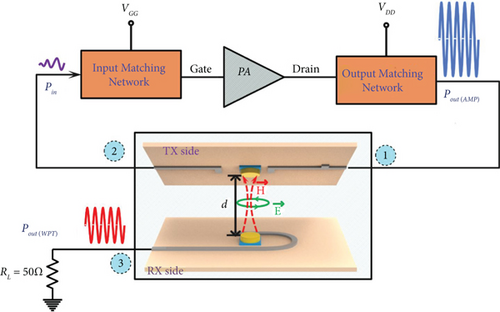
In contrast to our previous design [10], the proposed circuit of this work utilizes a three-port structure for signal generation and transmission, as shown in Figure 1. These ports are Port 1 (drain), Port 2 (gate), and Port 3 (output). Ports 1 and 2 are within the closed loop of the oscillator, while Port 3 serves as the receiving port for wireless power transfer.
2.1. Electromagnetic Simulation of the Feedback Network and WPT Structure
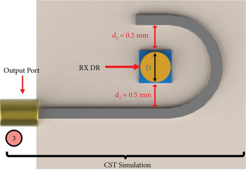
The dual-DR structure of Figure 1 has been numerically analyzed using CST Microwave Studio. Each DR is on an RO4003C substrate with a height of 0.812 mm, a copper thickness of 35 μm, and a relative permittivity εr of 3.55. The εr of the DR is 36.5, with a height and radius of 3.2 mm and 3.9 mm, respectively. Figure 2 illustrates the lower (Tx) and upper (Rx) substrates. The gray-shaded coupling transmission lines and DRs have been simulated in CST using a full-wave method. Afterwards, their computed S-parameters seen from the specified ports have been imported into ADS software as an S3P matrix and incorporated into the remaining parts of the circuit. This includes the transistor network and red transmission lines. Parameters d2 and d3 represent the spacing of the coupling microstrip lines to the DR edge on the drain and gate sides, respectively. An open-ended quarter-wave extension of the feed line ensures efficient coupling to each DR.

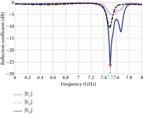
It is well-known that the drain load impedance and the impedance seen by the transistor gate have significant impact on the output power level. Therefore, the scattering parameters of Ports 1 to 3 must be determined and converted to the required impedances. Figure 3 illustrates input matching of these ports as a function of frequency. To achieve optimal performance in terms of the output power, a passive matching circuit on the drain and gate side is included to convert the port impedances to the required drain and gate impedances.
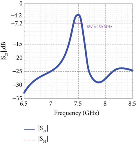
Part of the power generated at the output, that is, the drain of the transistor, is diverted through the feedback path to the gate to sustain the oscillation (S21), while another part is transferred to the output terminal (S31). To maximize power at the output of the WPT system, d3 was set greater than d2, to reduce the power in the feedback path and increase the transfer coefficient S31 to the output. The transmission feedback loss and transmission output gain are depicted in Figure 4a. In Figure 4b, the transmission coefficient S21 of the series-feedback DDRO from [10] has been added. This allows for a direct comparison with the proposed parallel-feedback structure, highlighting the improvement in power transfer efficiency.
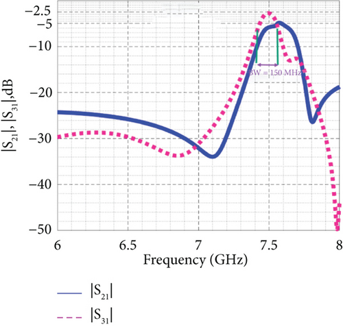
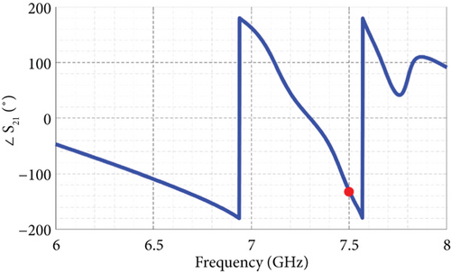
At a frequency of 7.5 GHz, the magnitudes of S21 and S31 are −6 and −2.5 dB, respectively. Therefore, a minimum gain of +6 dB is required for the transistor at this frequency to meet one of the oscillation conditions. In Figure 5, the calculated phase due to the WPT system is illustrated. At the working frequency, this phase will be added to the phase of the remaining systems of the loop to end up in a multiple of 2π.
2.2. Design Procedure for PA
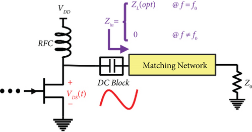
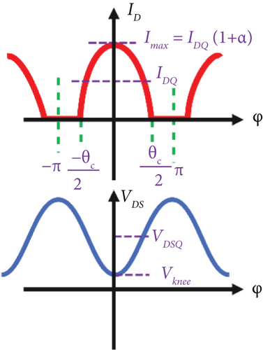
There are three key factors that must be considered when designing PAs: output power level, gain, and efficiency. Class AB PAs are often favored in amplifier designs, as they allow higher output power though at the expense of lower power gain [11, 12]. Figure 6a shows that the matching network in a PA is responsible for generating the optimum load impedance at the fundamental frequency (f0) and short circuits at the harmonics of the fundamental frequency. Under this theoretical condition, as shown in Figure 6b, VDS becomes sinusoidal.
It must be mentioned that the WPT circuit was meticulously designed to achieve a maximum |S31| parameter at 7.5 GHz (the same frequency as in [10]) while maximizing impedance matching at Ports 1 and 2. To further optimize power output of the PA, a load-pull analysis was performed in ADS software. This analysis determined the optimum drain load impedance by examining the load-pull contour diagram, which visualizes the impact of varying the load impedance on PA output power level and efficiency [13].
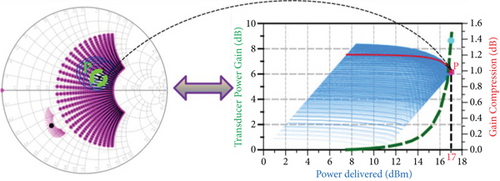
For the sake of a fair comparison, the total DC input power of the proposed circuit is set to be equal to the same power for the DDRO circuit previously presented in [10]. In other words, for a supply voltage of VDD = 3.3 V and a supply current of IDD = 26 mA, the DC input power of the DDRO of this work is equal to that of the circuit demonstrated in [10]. For these values of the supply voltage and current, the quiescent point of the transistor is determined, and the load power is computed according to Equation (5). This value will be 17 dBm. Now, Figure 7 illustrates the impedance contours obtained from a load-pull analysis for an output power of 17 dBm. This corresponds to a load impedance of ZLoad = 68.9 + j18 ohms and an input impedance of ZIn = 15.35 − j19.79 ohms.
3. Simulation Results
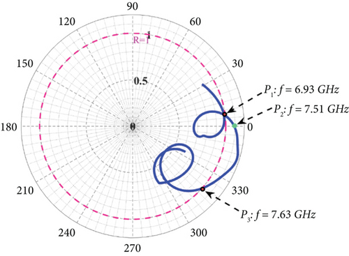
The polar plot representing the computed loop gain is depicted in Figure 8. It illustrates that the magnitude of the loop gain exceeds unity at a frequency of 7.51 GHz. Additionally, the phase reaches zero at this particular frequency.
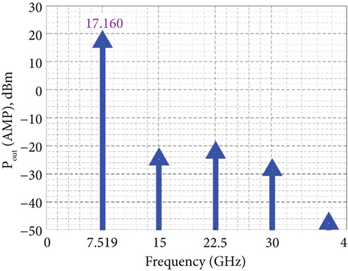
At a frequency of 7.5 GHz, compared to the series-feedback design in [10], which was a two-port network, the transmission coefficient has improved from |S21| = −4.2 dB (series-feedback network) to |S31| = −2.5 dB (parallel-feedback network), indicating an improved power transfer efficiency in the currently proposed design. A harmonic balance simulation is conducted in ADS, as illustrated in Figure 9. It is important to note that the maximum power output specified in the datasheet for the ATF26884 is 18 dBm at a frequency of 12 GHz [14]. Following the incorporation of impedance values obtained from load-pull analysis into the gate and drain terminals, as illustrated in Figure 2, the lengths of transmission lines l1, l2, and l3 have been optimized and trimmed to achieve the maximum power output of the PA.
4. Implementation and Measurement of the Proposed Parallel-Feedback DDRO
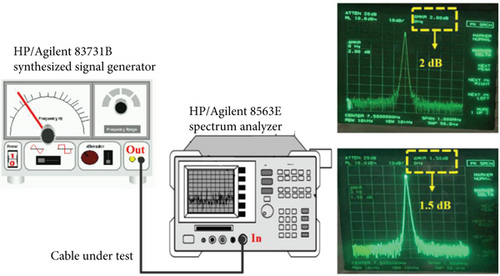
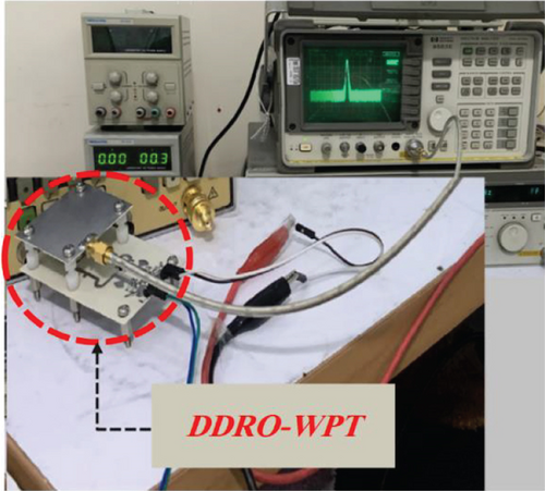
The measurements were conducted under standard laboratory conditions using recently calibrated RF equipment to ensure accuracy. The fabricated DDRO is seen in Figure 10. In contrast to [10], the RF chokes in this design are narrowband, aiming to reduce the transistor gain at adjacent frequencies. The output power level of parallel-feedback DDRO-WPT has been measured using an HP 8563A spectrum analyzer. The bias point is set at ID = 25 mA, VDD = 3.3 V, and VGG = −0.5 V. The losses of the coaxial cable connecting the DDRO to the spectrum analyzer have been measured at 7.5 GHz. For this purpose, the setup shown in Figure 10c was used. In this setup, a HP/Agilent 83731B synthesized signal generator and HP/Agilent 8563E spectrum analyzer are used to measure the total insertion loss of the cable under test, that is, including its connectors. The measurements show a total loss of 3.5 dB for this cable at 7.5 GHz. The circuit has been fabricated on RO4003C, as shown in Figure 10a,b. The bottom substrate, housing the power transmitter section and the transmitter DRO, measures 45 mm × 76 mm. The receive DR is located on the top substrate which measures 45 mm × 40 mm.
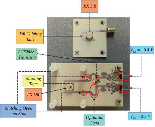
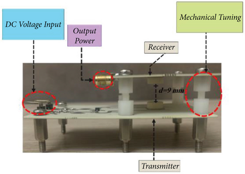
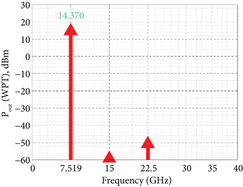
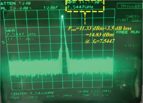
The impact of the interresonator spacing on the transfer efficiency has comprehensively been investigated in [8] and summarized in Figure 9 of [8]. According to [8], the power transfer efficiency remains nearly constant for an interresonator spacing less than 1.2D where D denotes the diameter of the cylindrical DR. Our measurement results have also revealed that the transmitted power remained relatively constant within the mentioned range. Hence, for the following measurements, the interresonator spacing was kept at a fixed value of 9 mm. In Figure 11, the measured power level for the parallel-feedback DDRO operating at 7.54 GHz is 11.33 dBm. Taking into account the cable losses, the power level at the output port was calculated to be 14.83 dBm. There is a very good agreement between the measured output power and the harmonic balance simulation results. Table 1 provides a comparison between our proposed circuit and the DROs reported in various references. To highlight the main difference between the reported DROs and our parallel-feedback DDRO, it should be noted that conventional designs commonly deliver their output power to a port which is in direct electric contact to the DRO, whereas in this circuit, the output signal is delivered wirelessly to a second DR acting as the receiver of a WPT system. According to Table 1, one should note that the DDRO of this work delivers a significant power level even in the presence of the WPT transmission losses.
| Reference | Transistor part | DRO type | Frequency (GHz) | Dielectric constant | Output power (dBm) |
|---|---|---|---|---|---|
| [15] | ATF26884 | Parallel | 9.683 | 30 | 9.310 (simulated) |
| [16] | ATF-36077 | Series | 10.698 | 95 | 8.66 (measured) |
| [17] | ATF-36077 | Parallel | 12.38 | 37.4 | 15.551 (simulated) |
| [18] | ATF13786 | Parallel | 5.8 | 36 | 10 (simulated) |
| [19] | AFP02N2 | Series | 26 | NM | 10.523 (simulated) |
| [20] | NE3210S01 | Parallel | 8.003 | 35–37 | 12.4 (NM) |
| [21] | BFP520F | Parallel | 7.99 | 29.5 ± 1 | 7.83 (measured) |
| [22] | NMa | Series | 9.6 | 38 | 7 (measured) |
| [23] | ATF-36077 | Series | 11.995 | 29.5 | 6.93 (simulated) |
| [24] | HBFPA450 | Series | 2.4 | NM | 7.902 (simulated) |
| [25] | BFR740L3RH | Parallel | 21.68 | 20 ± 1 | −5 (measured) |
| [10] | ATF26884 | Series | 7.507 | 36.5 | 13.07 (measured) |
| This work | ATF26884 | Parallel | 7.544 | 36.5 | 14.83 measurement |
- Note: Bold row indicates the performance of the proposed design reported in this work.
- aNot mentioned in the reference.
5. Conclusion
This paper reports the simulation and implementation of a WPT system based on a parallel-feedback DDRO configuration to deliver a higher output power level than our previously introduced circuit. In our previous work on DDRO appeared in [10], the power level at the output of the WPT system and the transmission bandwidth between the resonators were found to be 13.07 dBm and 150 MHz, respectively. Here, compared to [10], the wireless output power level and the DC-to-RF efficiency were increased by about 2 dB and 83%, respectively, while maintaining the same DC input power supply and the transistor type. It is noteworthy that this power upgrade was achieved without sacrificing bandwidth. While increasing the magnitude of both S21 and S31 can lead to a higher output power level, there exists a trade-off between these two parameters. An excessive increase in S21 can push the transistor into the compression region, hindering further output power enhancement. Our design exploits the unavoidable relationship between S21 and S31. By strategically increasing S31 via an optimized microstrip line coupling, the output power is enhanced, while a reduced S21 keeps the transistor outside compression. As demonstrated in Equation (6), this enhancement in S31 leads to a proportional increase in both the output power and the transmission efficiency. It has been demonstrated that load-pull analysis, for instance, in ADS software is of high importance for selecting the optimum output load and input impedance matching for maximum power output. In addition, optimizing the coupling distance between the microstrip transmission lines and the transmitter DR has further enhanced power transfer efficiency. Unlike the series-feedback approach, which relies on a lossy termination at the end of the feed line to generate negative resistance at the resonance frequency and suppress reflections outside the resonance band, the parallel-feedback topology eliminates this lossy element, leading to a higher efficiency and higher output power level. As a final remark, it must be mentioned that the improved power level of this work yields an improved DC-to-RF efficiency of 36.85% in contrast to our previous work of [10], where the DC-to-RF efficiency was 19.50%.
Conflicts of Interest
The authors declare no conflicts of interest.
Funding
No funding was received for conducting this research.
Open Research
Data Availability Statement
All data generated or analyzed during this study are available from the corresponding author on reasonable request.


