A New ZVT Quadratic High Step-Up Nonisolated DC-DC Converter
Abstract
This paper introduces a quadratic DC-DC converter that operates with zero-voltage transition. In this converter, the combination of integrated coupled inductor technique and diode–capacitor technique is employed to boost static gain and decrease voltage stress on the main switch. Moreover, with the help of a third winding wound on the main ferrite core and an auxiliary switch and diode, zero voltage transitions are provided for the main switch in a wide range of load variations. Furthermore, the auxiliary circuit in the converter exhibits a short conduction duration, resulting in negligible conduction losses due to the minimal circulating current. Additionally, both the auxiliary switch and diode achieve zero-current switching (ZCS), effectively eliminating switching loss. Moreover, the diode operates without reverse recovery issues, preventing any significant loss in the converter. These features have made it possible to design a converter with high voltage gain, high efficiency, and high power density. The fundamental operational principles of the converter are comprehensively elucidated, and an in-depth analytical assessment of its steady-state performance is conducted. In conclusion, a 200 W prototype has been implemented to validate the converter’s performance.
1. Introduction
Nowadays, ultra-step-up converters constitute a fundamental component of renewable energy systems [1]. Within these systems, the output voltage is generally low and needs to be increased for compatibility with the grid. Using a conventional boost converter comes with several disadvantages, including high voltage stress on power switches, high current stress on diodes, increased conduction and switching losses, and limited voltage gain [1, 2].
High-gain converters are categorized into two main types: isolated and nonisolated configurations. High-frequency transformers are utilized in isolated converters, leading to an increase in volume, weight, and cost. Consequently, nonisolated converters are more apt for low-power applications due to their inherent characteristics [3]. Many techniques are introduced to increase the level of output voltage [3–6]. One of these techniques is employing the source impedance converters [7].
Although Z-source converters enhance voltage gain, they come with significant drawbacks, including discontinuous input current and elevated switch maximum voltage, which are critical concerns [7–9]. In the quadratic Δ-source converters, the duty cycle is not limited, the input current maintains continuity, and the ground is common, but the switch voltage stress is high, the converter operation is complicated, and the voltage gain is relatively limited [10, 11]. Another approach involves the use of coupled inductors, which both enhance voltage gain and reduce the maximum voltage of the switch. However, the energy stored in the leakage inductance is released through the power switch, which raises the voltage spike. Therefore, to capture the mentioned energy in these converters, the use of clamp circuits or lossless snubbers is necessary. However, this adds complexity to the converter’s operation and increases the overall costs [12–15].
Employing the switched-capacitor circuits, whose operation is based on the charge-pump circuits, is another approach to enhancing the voltage gain in the DC-DC converters. This approach combines the capacitor, diode, and power switch to boost voltage gain. However, it results in reduced efficiency due to increased current stress on the power switches, as well as higher switching and conduction losses [16, 17].
Voltage multiplier cells provide an alternative method for boosting voltage gain, utilizing a combined setup of diodes and capacitors. Despite its straightforward design and high efficiency, this technique involves a large number of components, and the reverse recovery problems linked to the diodes can contribute to higher losses in the converter [18, 19].
The combination of the mentioned techniques is being used in some applications, such as the integration of coupled inductors and switched capacitors, combining the benefits of both techniques [20, 21]. A primary concern with high step-up converters is switching losses and the voltage surges on the power switches resulting from the transformer’s leakage inductance. Thus, different soft-switching techniques are introduced, which absorb the energy from the leakage inductors and facilitate soft-switching operation across all switching devices [22–25]. The zero-voltage transition (ZVT) is preferred over the zero-current transition (ZCT) technique because it eliminates capacitive turn-on losses. Converters [26–28] use a three-winding transformer configuration to improve voltage gain and alleviate switch stress, while an active clamp circuit is employed to enable ZV condition. This circuit not only enables ZV condition for all switches but also engages the transformer’s leakage inductance energy, effectively preventing voltage spikes across the switches.
In this paper, a quadratic DC-DC converter with low stress is introduced. The key contributions of the introduced converter lie in its configurable auxiliary circuit for providing zero voltage, which eliminates the need for additional auxiliary circuits when adding extra phases. Additionally, the auxiliary circuit’s low circulating current, due to the brief conduction duration of the auxiliary switch, helps improve efficiency. The circuit also facilitates soft switching for the semiconductor components while absorbing leakage inductance energy. A significant advantage of the design is the use of a single magnetic core to house all coupled inductors, leading to a substantial reduction in both the converter’s size and cost. Furthermore, in contrast to the active clamp circuit, the auxiliary MOSFET has its source grounded, which removes the requirement for isolating the gate drive circuit.
2. The Introduced Quadratic High Step-Up Converter
2.1. Overview of the Circuit
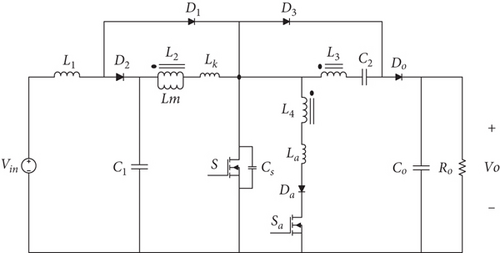
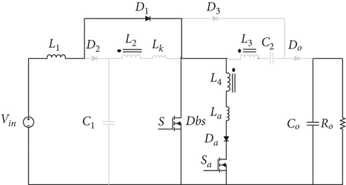
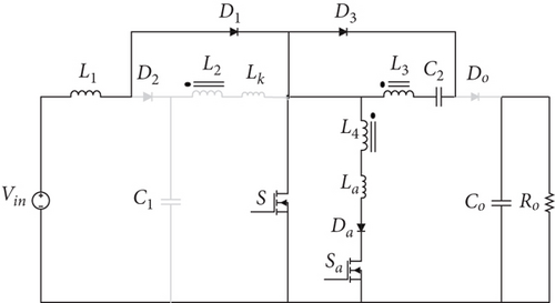
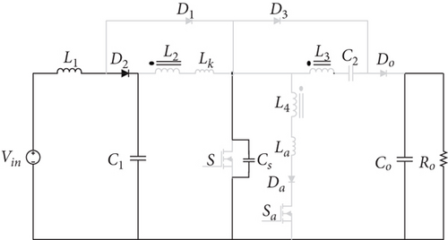
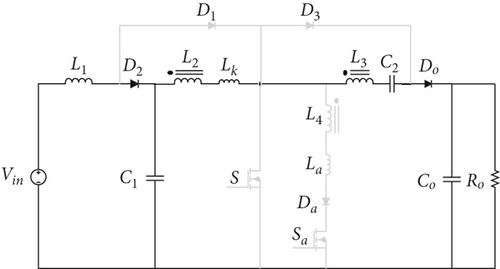
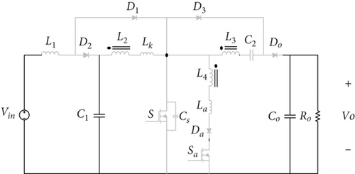
The introduced circuitry for the ZVT technique is depicted in Figure 1. The introduced circuit comprises a main switch (S); an input inductor (L1); a ferrite core (T), which contains three windings (L2, L3, and L4); diodes (D1, D2, D3, and Do); the storage capacitors (C1 and C2); and an output capacitor (Co). Also, to create the soft-switching conditions for all the semiconductor devices, a new auxiliary circuit is added to the converter, which consists of an auxiliary switch (Sa), an auxiliary diode (Da), a snubber capacitor (Cs), and an auxiliary inductor (La), which is wound on the core of the main circuit. The triple-winding coupled inductor is modelled by a magnetizing inductance (Lm) and leakage inductance (Lk).
2.2. Fundamental Operating Modes
- •
The L1 is sufficiently large, ensuring a constant current.
- •
The capacitors C1, C2, and Co possess sufficient capacitance, ensuring that their voltage levels remain unchanged during the entire switching period.
- •
All the semiconductor devices are ideal.
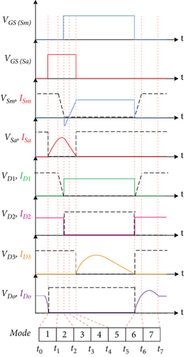
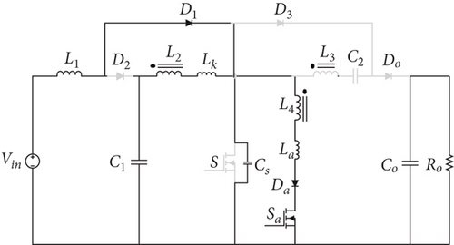
The suggested converter functions across seven distinct modes, accompanied by the corresponding key waveforms for these modes illustrated in Figure 2. In addition, the equivalent circuit of each operating mode is shown in Figure 3.
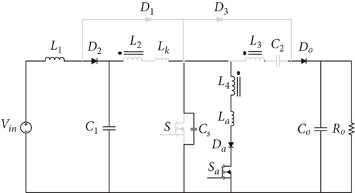
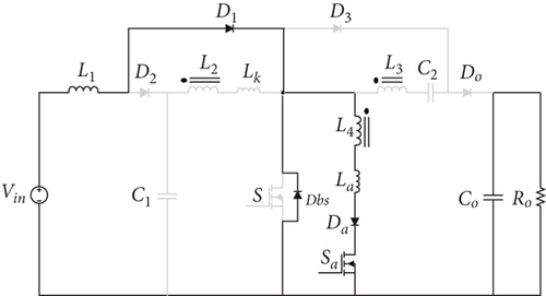
Before the commencement of the first mode, both the primary and auxiliary switches are in the off state. The diodes Do and D2 are in conduction, facilitating the transfer of input energy to the output.
Mode 4 [t3 < t < t4]: The current of the body diode reverses direction and gradually rises through the main switch, thereby facilitating zero voltage during the activation of the switch. Furthermore, owing to the linear reduction of the current through the auxiliary switch, its deactivation occurs under zero-current conditions, ensuring minimal switching losses.
Mode 5 [t4 < t < t5]: D3 conducts, maintaining a constant current through the main switch, which results in the charging of the magnetizing inductance. Do turns off, and the Co provides the current to the load. The inductor L1 is energized by the input voltage, while the L3 inductor charges C2 capacitor. This mode concludes as the S is switched off.
Mode 7 [t6 < t < t7]: When the output diode conducts, the energy of the L2 and L3 inductors supply the output current. When the auxiliary switch turns on again, this mode ends.
3. Steady-State Performance Analysis
3.1. Voltage Gain
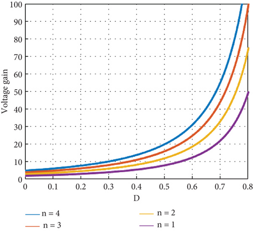
By neglecting the leakage inductances, the calculation of the voltage gain can be performed by applying the volt-second balance to L1 and Lm in continuous conduction mode (CCM). Since Modes 3, 4, and 6 are transition periods and too short, only Modes 1, 2, 5, and 7 are considered for steady-state analysis.
3.2. The Semiconductor Device Stress
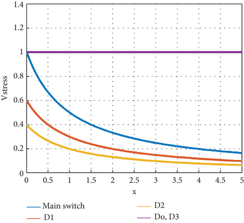
In order to illustrate the relative voltage stress of the switching elements versus the turn ratio of the introduced converter, Figure 5 is presented. A comparison between the voltage stress of the main switch and the D1, D2, D3, and Do diodes is shown in this figure. As observed, the least voltage stress belongs to the D2 diode, and the highest voltage stresses belong to the D3 and the output diode (Do). Between these two values, the voltage stress on the main switch exceeds that of the diode D1. The significant decrease of the voltage stress on the main switch leads to choosing a MOSFET with low drain-source resistance (RDS(on)). The lower conduction losses and the higher voltage gain for the converter could be obtained by using the MOSFETs with low RDS(on). Furthermore, there is low voltage stress on the D1 and the D2 input diodes. According to the ZCS operation for turning off these two diodes, and no reverse recovery problem for them, the conduction losses of these two diodes were reduced significantly. The maximum voltage of the output diode is significant, but the condition of zero current during both turn-on and turn-off limits its conduction losses. The output diode loss is calculated with details in Section 5.
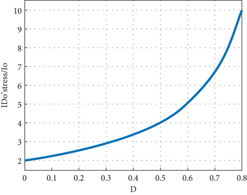
The normalized current stress of the output diode versus the duty ratio is shown in Figure 6. Whereby by raising the duty ratio of the main switch, the current stress on the output diode is increased. However, according to the high voltage gain of the introduced converter, the duty cycle value to reach a 400 V output voltage level is not that high.
3.3. Design Procedure
According to the converter operations, when the output diode turns off, the Co provides output current. Thus, the output capacitor can be designed by Equation (31).
3.4. Discontinuous Conduction Mode (DCM) Analysis of the Converter
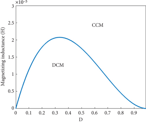
The introduced converter, in DCM, has an additional state, where both the switches and Do are off (Figure 7). As a result, the output capacitor supplies the load current. To analyze the converter in this mode, neglecting losses and obtaining the average current of L1 and L2 as well as calculating the mean current of the Do in DCM, the boundary operating range is determined in terms of the magnetizing inductance as seen in Figure 8.
4. A Comparative Analysis of the Introduced Converter and Other Similar Converters
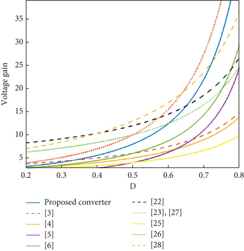
To conduct a comparison of the introduced converter with some recent converters, Table 1 is prepared. As shown in Table 1, the converters in [4, 22] have just one switch but operate under hard switching conditions with low switching frequency, which decreases the power density and efficiency significantly. The converter in [5] has the lowest number of elements in Table 1, which leads to the reduction of conductive losses and the converter cost, as well as minimal fluctuations in the input current and output voltage. But the converter operates under hard switching conditions, and the switches experience high voltage strain, which results in a rise in capacitive turn-on loss. In the converter [6], the input current ripple remains low, just as in the introduced converter, and the energy of the leakage inductance is recovered well, but the converter has a switch with a floating source, and the converter experiences significant switching losses owing to the hard switching operation. The greatest voltage gain and the least voltage stress belong to the converter [22]. But this converter, unlike the introduced converter, possesses many elements, switching losses, and input current ripple. The converters with soft-switching techniques in [23, 25] have high voltage gain and very low voltage stress on the switches, but the quantity of their components is high, leading to increased expenses and elevated conduction losses in the circuit. The converter in [24] comprises four switches, which make the control circuit operation more complex. The converter outlined in [24] has a lower voltage gain than the introduced converters in Table 1. The converter in [25] is a high step-up converter, but the converter has many disadvantages, such as discrete input current, a separate ground for the input and output side, and an existing floating source of power MOSFET, which makes it necessary to use isolated drivers. The auxiliary switch in the introduced converter [24, 25] turns on under ZC conditions, and the capacitive turn-on loss of the MOSFETs cannot be ignored. Ultimately, in comparison to the previous converters, the introduced converter features fewer components and high efficiency, shared ground, low ripple of the input current, and switches with grounded sources. Converter [26] exhibits a superior voltage gain compared to the introduced design, along with features such as ZV condition and reduced current ripple. However, it involves a larger number of components and incorporates three magnetic cores, contributing to increased size and weight. Converter [27] utilizes a Y-source network to enhance voltage gain, effectively achieving higher performance with fewer components. Nonetheless, the snubber capacitors associated with the switches are not accounted for in the component count, and soft-switching operation is compromised under light load conditions. Converter [28] demonstrates better performance in terms of both voltage gain and component count (with snubber capacitors excluded from the count) than the suggested converter. However, along with challenges with the active clamp circuit, there is no shared ground between the input and output of this converter, which may present integration challenges. Figure 9 illustrates the comparative voltage gain of the converters.
| Converter | Voltage gain | Voltage stress across switch | No. of elements | Specifications | ||||||||||
|---|---|---|---|---|---|---|---|---|---|---|---|---|---|---|
| MC | S | D | C | T | Po (W) | Vi (V) | Vo (V) | Effa (%) | Cost ($) | Size | SCb | |||
| [3] | 3 | 2 | 2 | 7 | 16 | 200 | 40 | 400 | 96 | 14.4 | High | ZVT | ||
| [4] | 2 | 1 | 4 | 5 | 13 | 200 | 25 | 400 | 96 | 15.3 | Med | ZCT | ||
| [5] | Vo | 2 | 2 | 2 | 2 | 8 | 400 | 62 | 250 | 91.5 | 11.4 | Med | Hard | |
| [6] | 2 | 2 | 5 | 4 | 13 | 200 | 40 | 380 | 94.7 | 12.3 | Med | Hard | ||
| [22] | 1 | 1 | 6 | 6 | 14 | 150 | 42 | 420 | 96.5 | 15.1 | Med | Hard | ||
| [23] | 3 | 2 | 6 | 7 | 18 | 200 | 30 | 380 | 95.3 | 14.6 | High | ZVT | ||
| [25] | 1 | 3 | 4 | 8 | 16 | 200 | 40 | 400 | 94 | 16.9 | Med | ZVT | ||
| [26] | 3 | 2 | 4 | 5 | 15 | 200 | 48 | 380 | 96 | 16.7 | High | ZVZC | ||
| [27] | 2 | 2 | 2 | 4 | 10 | 200 | 28 | 380 | 96 | 19.1 | Med | ZVT | ||
| [28] | 2 | 2 | 3 | 5 | 12 | 200 | 20 | 400 | 94 | 23.9 | Med | ZVT | ||
| Introduced converter | 2 | 2 | 5 | 4 | 13 | 200 | 20 | 400 | 95.2 | 15.4 | Med | ZVT | ||
- aEfficiency.
- bSwitching conditions.
5. Loss Analysis
Since D1 and D2 voltage stress is less than 200 V, Schottky diodes are used to reduce conduction losses while eliminating reverse recovery losses.
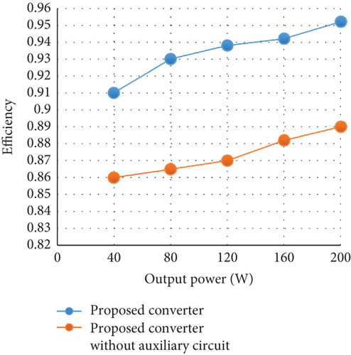
Based on the above calculations, the total converter power losses are 9.63 W for the 200 W full-load condition. As a result, a calculated efficiency of 95.18% is achieved. Figure 10a presents a comparative analysis of the efficiency of the introduced converter, both with and without the inclusion of the auxiliary circuit, across a range of varying output power levels. Additionally, the allocation of losses among the various components of the converter is presented in Figure 10b.

6. Experimental Results
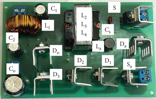
In order to validate the theoretical analysis of the converter, a 200 W prototype, depicted in Figure 11, has been constructed. The detailed specifications of the components utilized in the introduced converter for the laboratory prototype are listed in Table 2. The IRFB4668 type of MOSFET is used as the switch for its low RDS(on). For the D1, D2, D3, and Da, the MUR820 is used, and for the output diode, the MUR880 is used. In order to attain high efficiency, windings with several parallel liny wires are used in the coupled inductor.
| Symbol | Component | Specification |
|---|---|---|
| Vin | Input voltage | 20 V |
| Vout | Output voltage | 400 V |
| Pout | Output power | 200 W |
| f | Switching frequency | 50 kHz |
| C1, C2, Co | Capacitors | 10 μF |
| S | Main switch | IRFB4668 |
| Sa | Auxiliary switch | IRF840 |
| D2 | Diode | ST10100 |
| D1, Da | Diodes | MUR1520 |
| Do, D3 | Diodes | MUR860 |
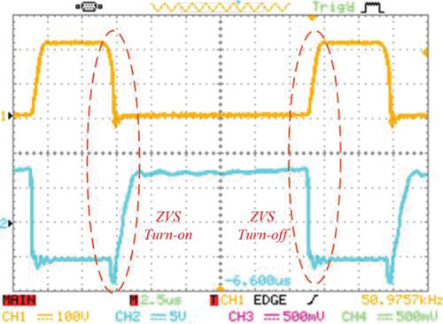
For the purpose of confirming the theoretical analysis, Figure 12 is presented. Moreover, Figure 12a shows the ZVS condition for turning on owing to the switch’s negative current, and following the snubber capacitor, the voltage across the switch increases at a gradual rate when the main switch is turned off.
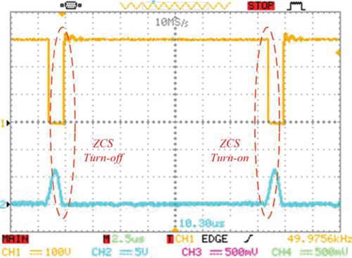
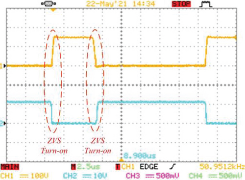
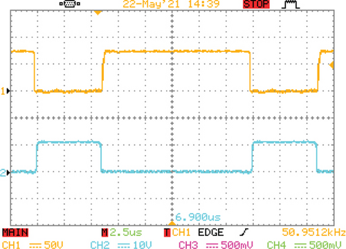
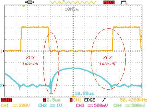
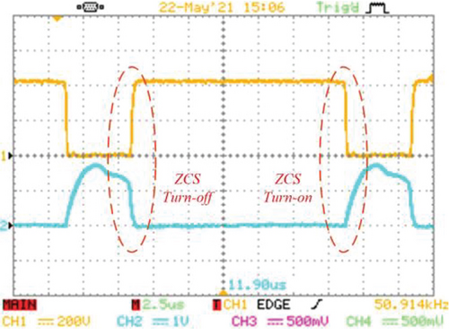
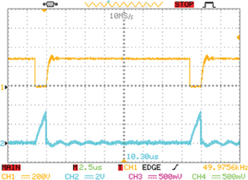
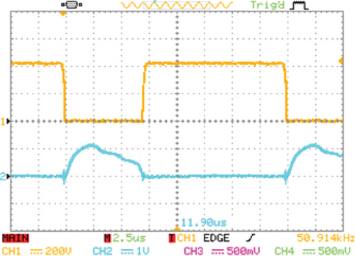
In Figure 12b, the auxiliary switch’s voltage and current are illustrated, which shows the ZCS operation for turning on and off because the auxiliary switch current rises and falls with a slope in turn-on and turn-off instances. Thus, both of the switches are operated under soft-switching conditions with no switching losses. According to Figure 12c, the ZVS operation is obtained for the D1 diode because of the gradual rise and fall of its voltage. As for the D3 and Do diodes, Figure 12d,e is presented, which shows the ZCS condition for both conduction and nonconduction states for these two diodes, which indicates that there is no reverse recovery problem in them.
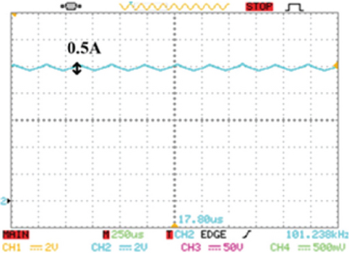
Figures 13a, 13b, and 13c illustrate, respectively, the current and voltage of the main switch, the auxiliary switch, and the output diode at the input voltage of 30 V. As can be seen, soft switching remains in these elements, and changes in load or input voltage have no effect on the soft-switching conditions of the converter, unlike the active clamp technique. In order to show the CCM operation of the converter, the input current of the converter is depicted in Figure 13d; here, the continuous input current is illustrated with a 10A average current and a 0.5A current ripple.
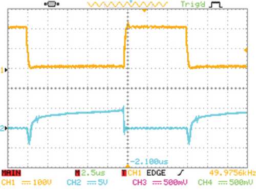
Remaining soft-switching conditions as input voltage and output load fluctuate, as well as reduced input current ripple, enhance the converter’s suitability for photovoltaic applications.
6.1. EMI Analysis
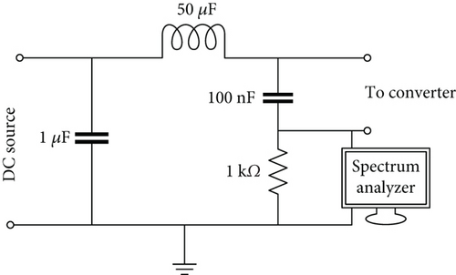
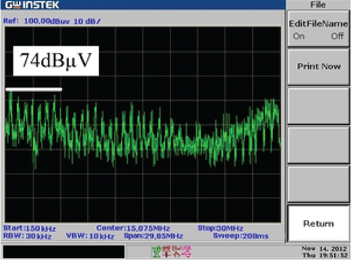
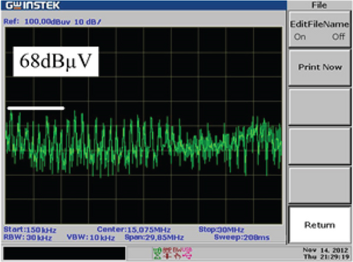
To assess the EMI of the converter, a line impedance stabilization network (LISN) block, denoted as Rs, is located between the input and the power supply. The LISN, as depicted in Figure 14, adheres to the CISPR22 standard. The main source of differential-mode noise, compared to common-mode noise, is observed in peak recognize mode. The EMI of the introduced converter was assessed, with Figure 15a,b displaying the EMI levels both in the absence and presence of the auxiliary circuit, respectively. In accordance with the CISPR22 standard, the vertical and horizontal axes are confined within ranges of 20–100 dBμV and 150 kHz–30 MHz, respectively. As shown in Figure 15b, the converter EMI is 68 dBμV, which represents a reduction of approximately 6 dBμV in comparison with the hard-switched configuration. As a result, applying soft-switching conditions resulted in a decrease in the EMI of the converter.
7. Dynamic Response and Stability of the Converter
Figure 16 demonstrates the dynamic behavior of the converter under both load and input voltage fluctuations. In Figure 16a, when the load decreases from full to half, the output voltage shows an overshoot of about 50 V that settles in 30 ms. In Figure 16b, as the load increases from half to full, the output voltage exhibits a 50 V undershoot, stabilizing at 35 ms. Moreover, Figure 16c depicts the output voltage’s response to a 15% input voltage variation. These results confirm the control circuit’s effective performance.

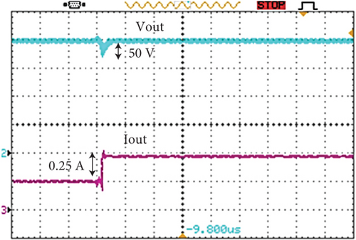
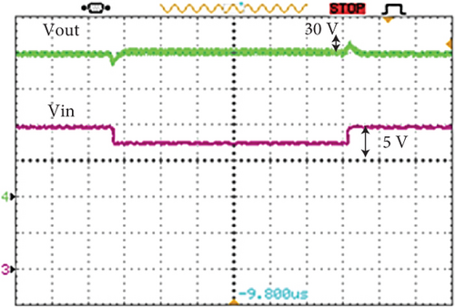
Figure 17 presents the Bode plot of the compensated transfer function (GC(S)) across different frequencies. According to control and dynamic system principles, the phase margin (PM) serves the converter’s stability. The diagram reveals that the converter demonstrates solid relative stability and satisfactory performance.

8. Conclusion
This paper presents a new ZVT quadratic boost converter with a new simple auxiliary circuit. Due to the low number of elements and current circulation in the auxiliary circuit, it does not impose significant conversion losses. On the other hand, all semiconductor elements of the circuit operate under soft-switching conditions. Moreover, the voltage stress on the main switch of the converter is considerably below the output voltage, which has led to the use of a low RDS(on) switch. Therefore, at full load, the converter achieves 95% efficiency, which is higher than similar converters. Furthermore, in terms of electromagnetic interference, the suggested converter features a 6 dBμV improvement over the hard-switched counterpart. Another key advantage is its low input current ripple, making it suitable for applications such as photovoltaics.
Ethics Statement
The authors have nothing to report.
Conflicts of Interest
The authors declare no conflicts of interest.
Author Contributions
All authors have contributed to this research. Alireza Abdollahi participated in formal analysis, investigation, methodology, software, and writing—original draft. Majid Delshad contributed to project administration, supervision, and validation, and Ramtin Sadeghi was involved in writing—review and editing.
Funding
This study did not receive funding from any sources.
Open Research
Data Availability Statement
The data used to support the findings of this study are included within the article.


