Secondary-Side Switching Control for Efficient Constant-Current Dynamic Wireless Charging
Abstract
Charge current and system efficiency are highly dependent on the load and mutual inductance, which change quickly during the dynamic wireless charging process, as the relative position between the primary coil and the secondary coil changes very fast. Due to the parameter tolerance and drift of the capacitor and inductor, the system detuning can also affect the charging current and system efficiency. This paper presents a novel switching-based secondary-side control strategy for dynamic wireless electric vehicle (EV) charging, aimed at achieving precise constant current (CC) charging and optimizing system efficiency under varying mutual inductance conditions. By dynamically adjusting the conduction angle (ϕ) and phase shift (θ) of the semiactive rectifier, the proposed method effectively eliminates secondary-side reactance, ensuring stable power transfer and high energy efficiency. An adaptive resonance tracking mechanism further enhances system performance by mitigating detuning effects caused by component tolerances and load variations. Extensive theoretical analysis, simulations, and experimental validation demonstrate that the proposed strategy achieves 92% system efficiency, ±0.05 A charging current fluctuation, and a rapid 3-ms response time, outperforming conventional approaches. These results validate the effectiveness of the proposed control method in improving charging stability, enhancing energy transfer efficiency, and ensuring robust operation in dynamic wireless EV charging scenarios, making it a promising solution for future wireless power transfer applications.
1. Introduction
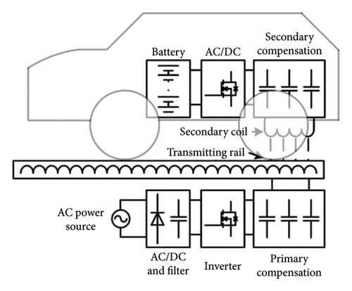
Dynamic wireless charging (DWC) system has the advantages of eliminating the twisted wires and supplying power during the running of electric vehicles (EVs) [1–5]. Then, the batteries installed on the EVs can be significantly reduced [6]. The structure of the traditional DWC system is shown in Figure 1. It mainly consists of two parts named as primary side and secondary side. The primary side converts the DC voltage obtained from the power grid and rectifier/filter into the alternative magnetic field. Through the magnetic coupler, the power is transferred to the secondary side. In the secondary side, the AC voltage is rectified and filtered and then supplied to the battery/supercapacitor. In general, constant current (CC) charging is required for quick charging for battery/supercapacitor [7, 8]. In this work, supercapacitor is used as the system load. The equivalent load resistance of supercapacitor varies with the charging time, which influences the charging current [9, 10]. In addition, since the mutual inductance of the DWC system may vary from zero to the maximum value during the driving of EVs [11–13], the charging current will also be influenced. Therefore, analysis and investigation of the closed-loop control method is essential to realize CC charging.
The most widely used method to realize CC charging is a secondary-side DC–DC converter. In [14], the secondary-side buck converter is used to adjust the charging current for the supercapacitor. The additional DC–DC converter significantly increases both the weight and volume of the receiver. To solve this problem, the secondary-side semiactive rectifier is proposed to regulate the charging current.
In [15], the charging current is regulated by adjusting the duty ratio of the semiactive rectifier. Compared to the buck converter, a semiactive rectifier can reduce an inductor and a filter capacitor, which are always bulky, especially when the power level is elevated. The defect of the method described in [15] is that the equivalent input impedance of the semiactive rectifier is not purely resistive, thus affecting the efficiency of the system. This work analyzes in depth the method for maintaining the pure resistive characteristic for the semiactive rectifier.
Usually, the system detuning caused by the parameter tolerance and drift of capacitors and inductors affects the resonant state of the system. As a result, the system efficiency is influenced, and the reactive power is also increased. To address this issue, an optimal reactance and resistance control strategy with an auxiliary measurement coil is used to track the maximum efficiency when the load varies and the detuning condition occurs [16].
By detecting the open-circuit voltage, the reactance component caused by detuning is eliminated. However, the rapidly changing mutual inductance condition in the dynamic wireless power transfer (WPT) is not taken into account. Particularly, the high-stability CC charging that is required for quick charging of supercapacitor needs to be further investigated [17–20].
In this paper, the switching system is designed to achieve the optimization of the CC charging and system efficiency. Based on the switching system theory, double state variables of the semiactive rectifier are applied to ensure the response speed and the pure resonant state for the secondary side.
- (i)
A novel switching-based secondary-side control strategy is proposed to achieve precise CC charging while maximizing system efficiency.
- (ii)
An adaptive resonance tracking mechanism is designed to ensure robust operation under varying mutual inductance conditions. Unlike conventional methods that suffer from power fluctuations due to detuning effects, the proposed strategy maintains optimal resonance, resulting in higher efficiency and improved system stability.
- (iii)
Extensive simulations and experimental validation demonstrate the effectiveness of the proposed method.
The rest of the sections are organized as follows. Section 2 presents the system’s theoretical analysis. Section 3 analyzes the switching model and operating principle of the semiactive rectifier. Section 4 gives the controller design and simulation results. Section 5 validates the proposed control method with experiments. Finally, the conclusions are drawn in Section 6.
2. System Structure and Theoretical Analysis
To systematically analyze the DWC system, this section first establishes the fundamental architecture and the mutual inductance model. Subsequently, the semiactive rectifier’s equivalent impedance characteristics are derived, followed by an in-depth exploration of the system performance under varying operating conditions.
2.1. System Structure and Analysis
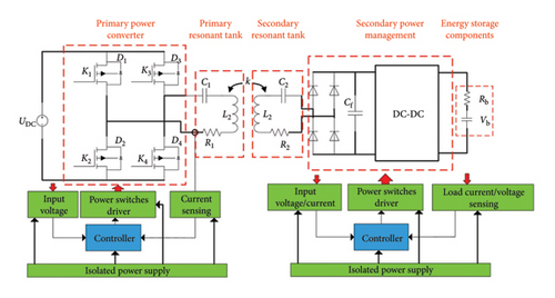
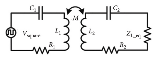
The structure of the DWC system is illustrated in Figure 2. The system consists of a primary side and a secondary side. The primary-side controller adjusts the power converter such as a full-bridge inverter to generate an AC voltage. Through the magnetic coupler, the secondary side receives the power that is transferred from the primary side, and then the AC voltage is rectified to the DC voltage. The secondary-side DC–DC converter adjusts the DC voltage and supplies to the system energy storage components. The fundamental wireless power link is presented via two coupled inductors and two capacitors connected as a series–series compensation topology as shown in Figure 3.
2.2. Analysis of the Secondary Semiactive Rectifier
As shown in Figure 4, the semiactive rectifier consists of two MOSFETs S1 and S2 with antiparallel diodes D3 and D4 in the lower part and two diodes D1 and D2 in the upper part. Co is the filter capacitor. Vb is the initial supercapacitor voltage, and Rb is the supercapacitor inner resistance. IO and UO are charging current and voltage for the supercapacitor, respectively.
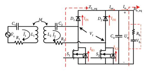
To focus on the control strategy analysis, the model assumes ideal diodes, MOSFETs, and capacitors, neglecting core losses and leakage inductance. This simplified model is experimentally validated and sufficiently supports control logic design [22]. The operating modes of the semiactive rectifier are shown in Figure 5.
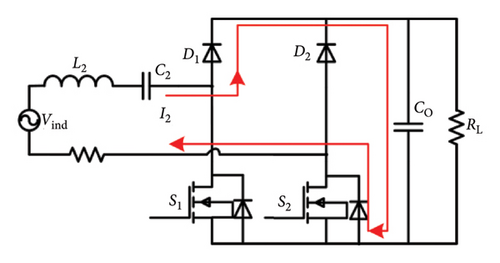
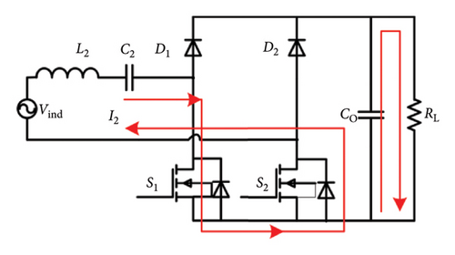
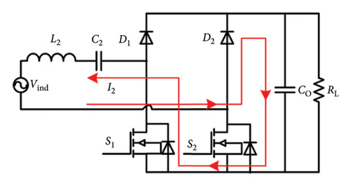
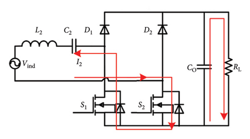
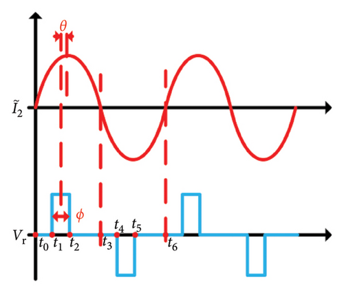
The input current I2 and voltage Vr of the semiactive rectifier are shown in Figure 6, where θ∈[−π/2, π/2] is the phase angle between I2 and Vr. ϕ is the conductive angle of Vr and expressed as ϕ = π(t2 − t1)/(t3 − t0) and ϕ∈[0, π].
2.3. System Performance Analysis
In the DWC system, system variables may vary with the secondary side moving along the power rail, such as mutual inductance and the primary and secondary reactance. The system parameters’ variety can affect the output current efficiently by adjusting the two controllable variables θ and ϕ. Thus, the output current can be adjusted.
Another noteworthy system performance is system efficiency, which can be obtained by calculating primary and secondary efficiency.
3. Secondary-Side Resonant State Tracking
This section proposes a switching control strategy to maintain the secondary-side resonant state. The method combines phase detection with tunable partition surfaces and can quickly adapt to mutual inductance changes and load dynamics.
3.1. Theoretical Analysis
According to (17), to achieve the optimization of the system efficiency, the secondary-side reactance X2 should be eliminated. By adjusting the phase shift angle θ, XL_eq, one can adjust it to –X2. Then, the secondary side operates in a resonant state, and the primary current is 90° ahead of the secondary-side inductive voltage . Furthermore, and are in the same phase, as shown in Figure 7.
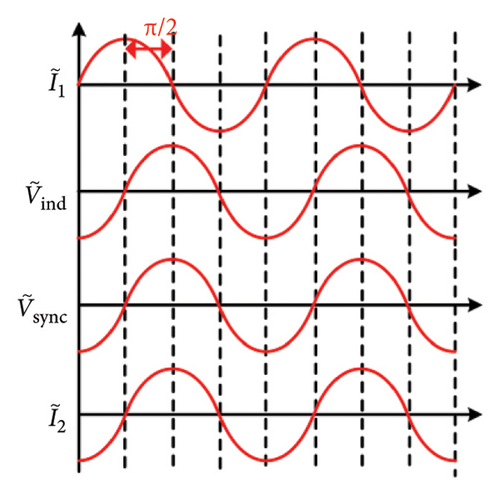

According to (22), and are in the same phase, and can be used as a reference to verify the secondary-side resonant state. Furthermore, if and are in the same phase, the secondary-side reactance can be eliminated and then the resonant state is ensured. In addition, since the detection transformer is a few turns and open-circuited, the influence of the detection transformer on the secondary side is little. In the following analysis, the phase angle between and is used as an input signal for the secondary-side controller for the resonant state tracking.
3.2. Analysis of the Switching System
To address the high response control speed as well as system efficiency optimization, a switching model of the semiactive rectifier was built, and then the corresponding control method was proposed. One period of the semiactive rectifier consists of four modes that can be classified by the operating state of switches and diodes. The corresponding waveforms are shown in Figure 9.
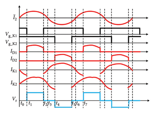
The detailed analysis of the four operating modes is listed in Table 1 and described as follows:
| Mode | Time interval | Current direction | Conductive components |
|---|---|---|---|
| 1 | [t0-t1] and [t2-t3] | Positive | K1 and K2 |
| 2 | [t1-t2] | Positive | D1 and K2 |
| 3 | [t4-t5] | Negative | D2 and K1 |
| 4 | [t3-t4] and [t5-t6] | Negative | K1 and K2 |
Mode 1 [t0-t1] and [t2-t3]: During this interval, K1 and K2 are turned on. The current flows through K1 and the antiparallel diode of K2. The battery is powered by a filter capacitor.
Mode 2 [t1-t2]: K1 is turned off and K2 is turned on. The upper diodes D2 are reverse-biased and current flows through D1 and the antiparallel diode of K2. The filter capacitor and load are powered by the energy transferred from the primary side.
Mode 4 [t3-t4] and [t5-t6]: During this interval, K2 is turned on and K1 is turned off. The current flows through the antiparallel diode of K1. The battery is powered by the filter capacitor.
Mode 3 [t4-t5]: The resonant current flows through the upper diode D2 and K1. The filter capacitor and load are powered by the energy transferred from the primary side.
- (i)
Current–power coupling: directly determines power transfer via , with its phase θ controlled by the switching surfaces K1 x + m1 = 0.
- (ii)
Resonance maintenance: The dynamics ensure secondary-side resonance conditions through Mode 2/3 transitions (see Figure 10).
- (iii)
Load regulation: It couples with the supercapacitor via Io = (Vco − Vb)/Rb, where ϕ adjustment stabilizes the output current.
These interactions form a hybrid dynamic system where the switching conditions in Table 2 enforce optimal energy transfer.
| i | Ai | bi | |
|---|---|---|---|
| 1 | |||
| 2 | |||
| 3 | |||
| 4 |
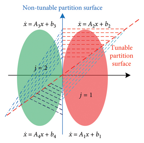
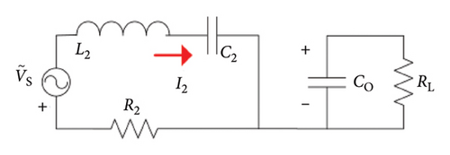
The switching system with double state variables is shown in Figure 11, where j represents the cell number and the activated subsystem dependents on the input logic(s). The subsystems that are constrained by the matrices and logic-input/state are listed in Table 2. In this work, bi is a fixed term representing the DC voltage source , which remains constant during operation. Control inputs are realized through state-dependent switching, via φ(x(t), s(t), and parameter adaptation, via ϕ-θ adjustment, ensuring robust regulation without requiring bi to vary.
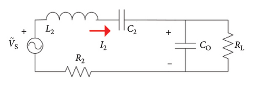
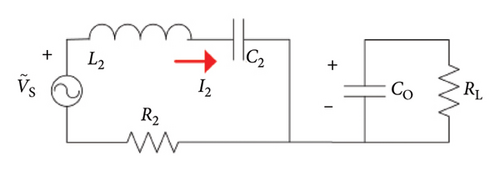
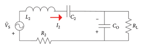
| i | |||
|---|---|---|---|
| 1 | |||
| 2 | |||
| 3 | |||
| 4 |
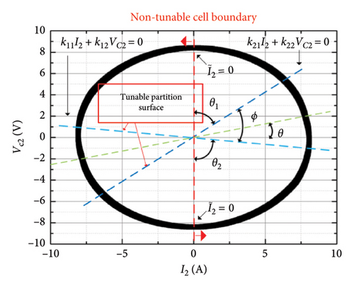
The nontunable cell boundary and designed partition surface for the reduced switching system are listed in Table 3.
The logic signal s that contains the information of both drive signals for switches and the operating state of diodes is shown in Figure 10. The signals K1 and K2 are synchronized with the designed partition surface, and the control signal can be considered as a series sign function of the designed surface in the reduced state space of the switching system.
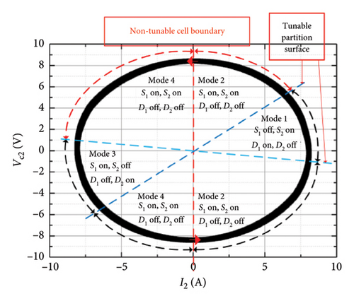
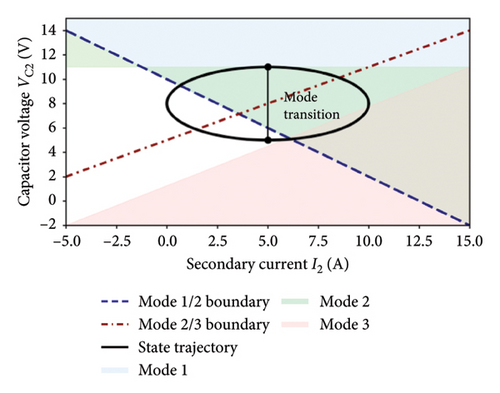
As shown in Figure 13, the state trajectory in the - plane demonstrates how the system dynamically transitions between operating modes. The elliptical trajectory confirms stable limit cycle behavior, with mode transitions occurring when the state crosses the designed switching boundaries (dashed lines).
As shown in Figure 14, through adjusting the partition surfaces parameters k11, k12, k21, and k22, the charging current is regulated and the secondary-side reactance X2 can be eliminated.
4. Controller Synthesis and Simulations
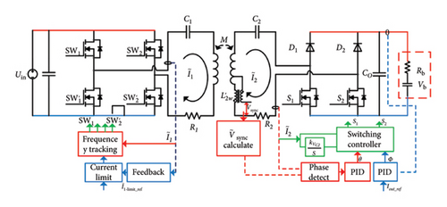
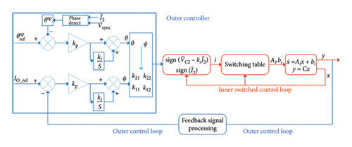
To validate the proposed control scheme, in this section, a dual-loop controller is developed, and MATLAB/Simulink simulations are performed. This work systematically addresses key challenges such as signal oscillation and sliding mode instability. In Figure 15, we analyze the secondary-side controller that is used to track the secondary-side resonance state and realize the CC charge of supercapacitors. measured by the hall-current sensor and obtained by the detection circuit are sent to the phase detection part. Then, two PI controllers, namely, θ and ϕ of the switching controller, are combined to control the semiactive rectifier.
-
Step 1: Signal acquisition
- •
Measure the secondary-side resonant current via a hall-effect sensor.
- •
Extract the synchronization voltage from the detection coil.
- •
-
Step 2: Phase detection
- •
Calculate the phase difference θ between and using a zero-crossing detector (equation (19)).
- •
-
Step 3: Resonance tracking
- •
Adjust the tunable partition surfaces (k11, k12, k21, k22) via PI_1 controller to eliminate secondary-side reactance X2 (equation (26)).
- •
Ensure and remain in-phase, maintaining the resonant state.
- •
-
Step 4: CC control
- •
Regulate the conduction angle ϕ via PI_2 Controller 2 based on the error between the measured Io and the reference current Iref (equation (8)).
- •
-
Step 5: Switching logic generation
4.1. Secondary-Side Control Scheme for Semiactive Rectifier
The secondary-side control scheme composed of the inner and outer loops is shown in Figure 16. For the inner loop as the switching controller, its inputs are the state variables and slopes of the partition surface k11, k12, k21, and k22. For the outer control loops, two PI controllers are designed to adjust the slopes of the partition surface (PI_1) and regulate Io for the supercapacitor (PI_2), respectively. The PI_1 controller is used to track the secondary-side resonant state and its input is the phase angle between and . The PI_2 controller is designed to achieve CC charging for a supercapacitor, and its input is the measured Io.
Based on the MATLAB simulations, the feasibility of the control scheme shown in Figure 17 is verified. It is obvious that the PWM signals (S1 and S2) have the problem of oscillation at the rising and falling edges, which is mainly caused by the fast switching actions.
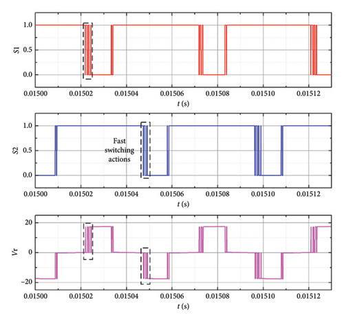
During the design of the secondary-side controller, the risk of the occurrence of sliding modes should be fully considered. When the system trajectory evolves on a sliding mode, the switching signal changes rapidly among its possible values. This can lead to system instability and component damage. Therefore, a frequency-limiting approach is proposed to address the above problem.
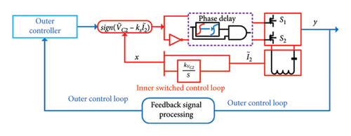
As shown in Figure 18, a frequency synchronization circuit is included in the control scheme. The voltage of the secondary-side compensation capacitor is estimated by the current sensor and the integrated circuit. The simulation results shown in Figure 19 indicate that the improved secondary-side control scheme can avoid the oscillation problem.
4.2. System Theoretical Simulation
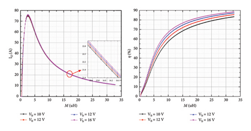
By using the parameters listed in Table 4, the output current and system efficiency under the open loop condition are calculated as the mutual inductance changes. The results are shown in Figure 19.
| Symbol | Parameter | Value |
|---|---|---|
| C1 | Primary resonant tank capacitor | 400 nF |
| L 1 | Primary resonant tank inductor | 160 μH |
| f 0 | Operating frequency | 20 kHz |
| C2 | Secondary resonant tank capacitor | 370 nF |
| L 2 | Secondary resonant tank inductor | 168 μH |
| C o | Output filter capacitor | 500 μF |
| R 1 | Primary coil inner resistance @20 kHz | 151 mΩ |
| R 2 | Secondary coil inner resistance @20 kHz | 72 mΩ |
| R b | Battery inner resistance | 10 mΩ |
| V s | Primary voltage | 50 V |
As can be seen from Figure 19, the output current varies widely when the mutual sensation changes. Under the same conditions, the higher the battery voltage, the lower the output current will be. The efficiency of the system also exhibits similar characteristics. To verify the output current regulation ability of the active rectifier, two adjustable parameters of the rectifier are calculated. The phase shift angle θ is set to 0, and the change of the corresponding system efficiency with ϕ is shown in Figure 20.
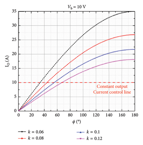
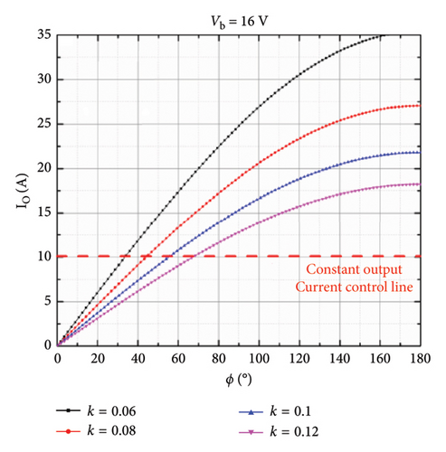
As shown in Figure 20, the output current can be adjusted to a constant value through changing the conduction angle ϕ. Before setting up the system, the CC control line must be set up in consideration of the degradation of system performance caused by the change of mutual inductance and load characteristics. For example, when the battery voltage is 10 V, the coupling coefficient k = 0.1, and the maximum output current of the system is about 2 A, and the CC control line should be lower than 2 A. Theoretical simulation verifies the output current regulation capability of the active rectifier under battery load.
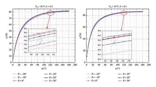
Moreover, under the same conditions, the phase shift angle θ is considered to calculate the efficiency improvement ability of the system. When the condition of the battery voltage Vb = 10 V and Vb = 16 V and the coupling coefficient k = 0.1, five groups of phase shift angles are selected to calculate the system efficiency against the conducting angle. Based on the simulation results displayed in Figure 21, the system efficiency increases while θ changes from −20° to 10°. The efficiency decreases when θ varies from 10° to 30°. The simulation results confirm that the imaginary part of secondary impedance reduces the system efficiency.
4.3. Optimized Secondary-Side Control Scheme
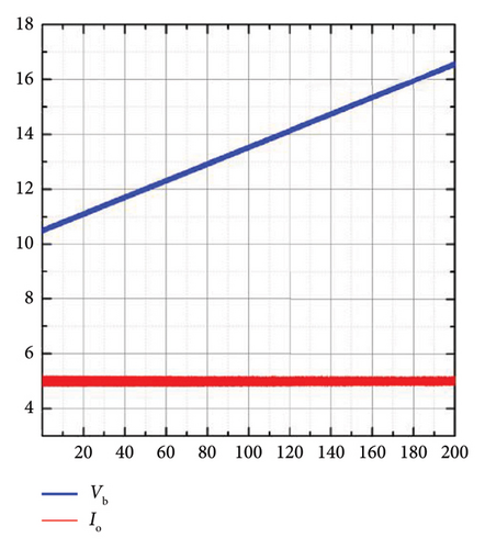
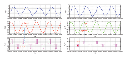
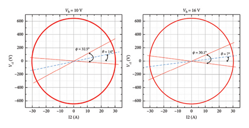
The improved secondary-side control scheme is further verified, and the simulation results are shown in Figure 22. As shown in Figure 22(a), the charging time is 200 s, and the charging voltage of the supercapacitor is 10 v ∼ 16 v. The initial voltage of the supercapacitor is 10 V, the ideal capacitance is 165 F, and the coupling coefficient k = 0.1. Over the time span of 200 s, Io remains at 5 A, and supercapacitor voltage increases linearly, which is consistent with the supercapacitor charging profile. It can be seen from Figure 22(b) that the phase difference of the resonant current on the primary side and the secondary side is 90°. Then, the secondary-side resonant state is verified. As shown in Figure 22(c), when the supercapacitor voltage increases from 10 V to 16 V, ϕ changes from 32.5° to 30.1° and θ from 14° to 7°, respectively.
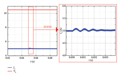
To further verify the dynamic response of the proposed secondary-side control scheme, the variation of mutual inductance is simulated by MATLAB software, as shown in Figure 23. It is clear that Io is still maintained at 5 A, when the mutual inductance varies from 30.84 to 25.68 μH for 0.05 s and the response time is 3 ms.
5. Experimental Verification
The feasibility of the proposed WPT system is verified by massive experiments. The experimental settings in the laboratory are illustrated in Figure 24, and the main system parameters are detailed in Table 4.
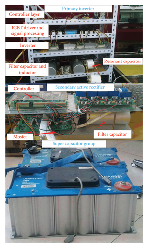
As depicted in Figure 24, power is supplied from the system’s DC voltage source to the H-bridge inverter. The DC voltage is converted into an AC voltage, which is then transferred to the secondary side via the designed magnetic coupler. On the secondary side, a semiactive rectifier consisting of MOSFETs (Infineon IPW60R041C6) and diodes (Fairchild RHRP3060), together with a capacitive filter (film capacitor), converts the AC voltage back to DC. This DC voltage is then delivered to the supercapacitor load.
The proposed switching control strategy, designed for achieving CC charging and optimizing system efficiency in the secondary-side semiactive rectifier, is implemented on a dual-core processor (EP4CE6 series FPGA + STM32F103 series ARM). The system load consists of two UCM48V165F supercapacitor modules. In addition, the PWM signal generator and overcurrent detection algorithms for the H-bridge inverter are executed on a DSP-28335 microcontroller located on the primary side.
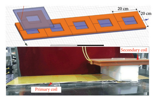
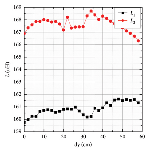
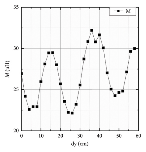
As shown in Figure 25, the primary coil consists of five series independent coils, each independent coil is 20 cm by 20 cm, and wound 10 turns with Litz wire. The secondary coil is wound 22 turns and the dimension is 20 cm by 20 cm with Litz wire, and the magnetic cores are used to enhance the magnetic field. The conventional coupler structure was selected as a foundational platform for validating the proposed control strategy due to its advantages, such as maturity, compatibility with the system’s power level, and ease of integration. Based on the magnetic coupler prototype shown in Figure 25, the self-inductance and mutual inductance parameters were measured experimentally to validate the design depicted in Figure 26. The self-inductance and the mutual inductance change in a certain range as the secondary coil moves along the primary coil. The proposed control method is to maintain the output current and improve the efficiency of the system when the secondary self-inductance changes.
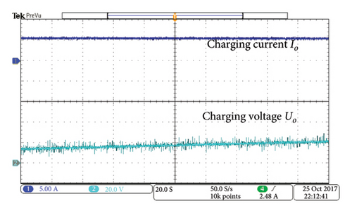
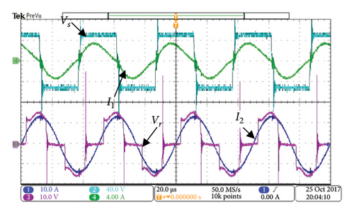
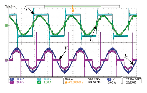
The experimental waveforms are captured by using a Tektronix Oscilloscope MDO3045B. Figures 27(a) shows the experimental results of Io and Uo with a charging time of 200 s. It is obvious that Io remains constant and the increment of Uo is 6 V, which coincides with the charge curve of the supercapacitor. Thus, the CC charging achieved by the secondary-side semiactive rectifier is verified. As shown in Figures 27(b) and 27(c), the phase shift angle θ of the semiactive rectifier is adjusted to achieve the CC charging. In the Figures 27(b) and 27(c), cyan color is the H-bridge inverter’s output voltage Vs, green color is the primary-side resonant current I1, blue color is the secondary-side resonant current I2, and purple color is the semiactive rectifier’s input voltage Vr.
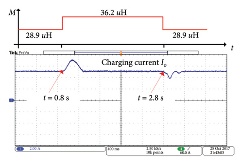
For the DWC system, the mutual inductance M varies during the EV’ movement. In Figure 28, the experiment takes into account the dynamic performance in the presence of a pulse change of mutual inductance from 28.9 to 36.2–28.9 μH at 0.8 and 2.8 s, respectively. During the experiment, the mutual inductance M is changed by changing the relative position between the primary coil and the secondary coil, and the value of M at each relative position is pretested. Then, the influence of M on the charging current Io is investigated. The experimental results are shown in Figure 28. It is clear that when M varies, the proposed control method can realize CC charging with a higher response speed.
Our experiments show that system efficiency remains relatively stable within a certain range of M. When M decreases by 20% from its nominal value, efficiency drops slightly by approximately 1.5%. Conversely, when M increases by 20%, efficiency improves by about 1.2%. This is primarily due to changes in the reflected impedance affecting power transfer capability.
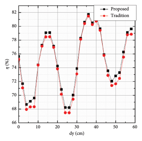
To validate the system efficiency improvement of the proposed control strategy, a traditional active rectifier is employed. By adjusting the pulse width of the active rectifier, CC charging can be achieved without the phase shift associated with the secondary current of the semiactive rectifier. The system efficiencies between the traditional and the proposed active rectifier are compared in Figure 29 with the battery voltage of 10 V. Note that the system efficiency is DC–DC efficiency. As shown in Figure 29, the traditional active rectifier has a lower efficiency due to the detuning condition caused by the resonant capacitor drift. The results show that the proposed control method can significantly improve the efficiency of the system. Compared to the traditional active rectifier, the efficiency improvement of the optimized active rectifier is mainly due to the pure resonant state control on the secondary side.
The performance of the proposed switching control strategy is compared with previous representative works in Table 5, where quantitative metrics demonstrate its superiority under complex disturbances. Compared to recent studies, our switching-based control strategy for dynamic wireless EV charging exhibits significant improvements in system efficiency, charging current stability, and dynamic response time, making it well-suited for real-world applications. The proposed method achieves 92% system efficiency, surpassing existing approaches, which range from 85% to 90%, demonstrating its effectiveness in optimizing energy transfer. In addition, the system maintains a charging current fluctuation of only ±0.05 A, which is significantly lower than the other methods (±0.1 A to ±0.3 A), ensuring more precise CC control and enhanced charging stability under varying mutual inductance conditions. Furthermore, the proposed approach exhibits the fastest dynamic response at 3 ms, outperforming existing techniques that require 4.5–10 ms, thereby ensuring rapid adaptation to mutual inductance variations and maintaining stable power delivery. These results validate the advantages of our optimized switching-based secondary-side control strategy, reinforcing its potential for efficient, stable, and highly responsive WPT in dynamic EV charging applications.
6. Conclusions
This study proposes an optimized switching-based control strategy for dynamic wireless EV charging, aiming to improve system efficiency, charging current stability, and dynamic response time. The proposed rectifier integrates an optimized switching-based control mechanism that dynamically adjusts the duty cycle in response to variations in mutual inductance and load conditions. Unlike conventional rectifiers that operate with fixed or predefined control parameters, our method enhances adaptability and minimizes conduction losses, thereby improving overall efficiency. Experimental and comparative results demonstrate that the proposed method outperforms existing approaches in terms of system efficiency, charging current stability, and dynamic response time, with corresponding improvements of at least 2%, ±0.05 A, and 1.5 ms, respectively. These findings validate the effectiveness of the optimized switching-based control strategy and highlight its potential for real-world applications in dynamic wireless EV charging scenarios. Future research will focus on further optimizing the control algorithm to enhance adaptability and exploring its applications in other WPT systems to expand its impact.
Conflicts of Interest
The authors declare no conflicts of interest.
Funding
This work was supported by the Basic Research Project of Liaoning Province under grant no. JYTMS20230453.
Acknowledgments
This work was supported by the Basic Research Project of Liaoning Province under grant no. JYTMS20230453.
Open Research
Data Availability Statement
The data that support the findings of this study are available from the corresponding author upon reasonable request.


