A Wideband Eight-Element Antenna Array With Metal: Frame for 5G New-Radio Applications
Abstract
In this paper, the study focuses on metal frame smartphone antennas and presents the implementation of an eight-port broadband MIMO metal frame antenna array for smartphones. The MIMO antenna operates within a wide frequency band ranging from 3.23 to 6.45 GHz, covering the 5G New Radio (NR) band N78 (3.4–3.6 GHz), 5G China band N79 (4.8–5 GHz), and IEEE 802.11ac band (5.15–5.35 GHz and 5.725–5.85 GHz). The novelty of this work lies in the use of dumbbell-shaped defects within a Defected Ground Structure (DGS), which significantly enhances isolation between antenna elements. Each compact antenna element features a stepped radiator and stub, arranged orthogonally at the corners of the array. Through evolutionary design and optimal parameter analysis, we investigate the principles of antenna operation. The results exhibit that the measured isolation between any two antenna elements is superior to 15 dB and the measured reflection coefficients are below −10 dB. The measured overall radiation efficiency of the antenna exceeds 60%, and it is even higher than 75% within the frequency ranges of 3.4–3.6 GHz and 4.8–5 GHz, specifically. Several indicators, such as the envelope correlation coefficient (ECC), diversity gain (DG), total active reflection coefficient (TARC), and mean effective gain (MEG), confirm the antenna’s robust MIMO performance, with strong correlation between simulation and measurement.
1. Introduction
With the rapid development of wireless communication technology, the fifth-generation (5G) mobile communication system, which boasts higher data rate and lower latency, has been widely promoted and applied in various applications [1–3]. Two main frequency groups are being adopted, namely sub-6 GHz and millimeter-wave (mm-wave) bands. Meanwhile, the increasing demand for data capacity in wireless communication and the trend of miniaturization of devices pose significant challenges for antenna design in achieving compact size with high data rate handling capability.
MIMO antenna technology, which involves using multiple antennas simultaneously for signal transmission and reception, can significantly enhance system capacity and spectrum efficiency. Hence, it is regarded as a core technology for 5G [4]. Due to the limited space on the smartphone’s mainboard and the requirement for multiple antennas in MIMO technology, integrating antenna elements onto the smartphone’s frame is essential. This approach maximizes the utilization of the limited space on the smartphone to accommodate more antenna elements, effectively addressing the issue of insufficient space on the mainboard. However, placing MIMO antenna elements close to each other can lead to strong signal correlation, thereby reducing the effectiveness of MIMO. In other words, mutual coupling decreases as the separation between antenna elements increases. Therefore, designing a MIMO antenna with an extremely compact structure and a low mutual coupling poses a challenge [5, 6].
Successfully implementing spatial diversity in a MIMO antenna system requires reducing mutual coupling and improving isolation between antenna elements, which is a crucial task. To enhance antenna performance, various decoupling solutions have been proposed, including the utilization of Defected Ground Structures (DGS) [7–9], neutralization lines [10, 11], self-decoupling, and orthogonal modes [12, 13].
In [14], good impedance matching on the desired frequency bands is achieved by loading stub onto the feed lines. In [15], the use of inverted C-slotted stub and T-slot has broadened the bandwidth, and a slit is adopted to enhance the isolation between the elements located along the printed circuit board (PCB) width. In [16], M-shaped slots serve as DGS between two adjacent antenna elements on the ground plane, enhancing isolation between these elements. In [17], the introduction of DGS alters ground currents to adjust resonance, reducing current coupling between antenna ports. Additionally, in [18], open-ended slots act as DGS to attain compact dimensions and enhance isolation between antenna elements.
In this work, the designed eight-element antenna comprises eight identical elements positioned orthogonally at four corners, and stub and DGS are simultaneously introduced to achieve optimal performance, characterized by high isolation, high gain, and low envelope correlation coefficient (ECC). This design enables high transmission rates and large channel capacity. The proposed antenna array consists of stepped radiators and stubs. Various evaluation structures and optimal parameter analyses were conducted for the proposed eight-port broadband MIMO antenna array.
2. Antenna Structure
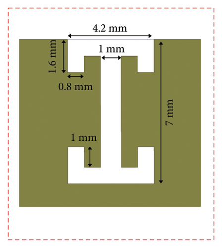
The geometric structure of the proposed eight-port ultra-wideband MIMO antenna array is illustrated in Figure 1(a). The PCB consists of two types: a main board and four side boards. The main board dimensions are 148.4 mm × 73.4 mm × 0.8 mm; the dimensions of the long sideboard are 150 mm × 7 mm × 0.8 mm, and the short sideboard dimensions are 75 mm × 7 mm × 0.8 mm. Both the main board and sideboards are printed on an FR4 substrate, with εr = 4.4 and tanδ = 0.02, adhered together using conductive adhesive. Figure 1(b) depicts the detailed dimensions of a single antenna element. Figure 1(c) illustrates the detailed dimensions of the dumbbell-shaped defect structure. Figures 1(d) and 1(e) show the side views of the antenna system.
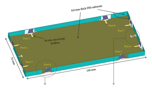



Each antenna element consists of a stepped radiator and stub, excited through a 50 Ω microstrip line (1.5 mm × 8 mm) and an SMA connector mounted on the back of the substrate. The dimensions of a single antenna element are 6.95 mm × 6.2 mm. Eight antenna elements are printed on four sideboards, which are vertically fixed to the main board, with two antenna elements printed on each sideboard. The eight antenna elements are arranged in pairs perpendicularly at the four corners of the system circuit board to minimize mutual coupling caused by their proximity. This arrangement enhances the isolation between Ant. 1 and Ant. 2, Ant. 3 and Ant. 4, Ant. 5 and Ant. 6, as well as Ant. 7 and Ant. 8. Additionally, the ratio between the distance of each vertical antenna element to the adjacent corner of the dielectric board and the distance of each horizontal antenna element to the adjacent corner is maintained at 1:2. This arrangement ensures the required isolation between adjacent antenna elements and leaves ample space for 2G/3G/4G or other wireless communication antennas within the smartphone.
Based on the designed antenna element, an eight-element MIMO antenna system for 5G metal frame smartphones was constructed. To understand the operational mechanism of the MIMO antenna system, research was conducted on the evolutionary design of the antenna elements, simulation of surface current distribution, and optimal parameter analysis. Three key variables (L, H, and S) significantly impact antenna performance and will be analyzed in subsequent sections.
3. Antenna Analysis
3.1. Design Evolution
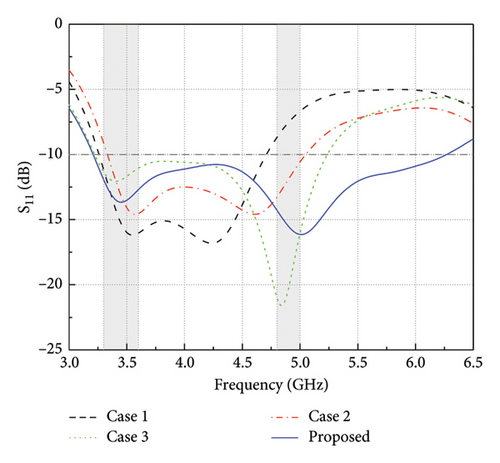
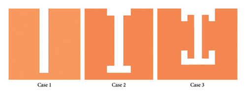
In Figure 2, Case 1 represents a simple notch rectangular antenna. By segmenting three small rectangles from Case 1, a stepped antenna, Case 2, is obtained. By making three small rectangular cuts in the radiator, the current path is extended, which broadens the antenna’s bandwidth and shifts its center frequency. Further removal of two rectangles from the antenna framework of Case 2 forms a complementary stepped antenna, Case 3. By creating a complementary stepped profile, the antenna’s bandwidth is significantly enhanced. Moreover, the stepped complementary structure effectively channels the flow of current, enhancing its concentration. Additionally, the complementary stepped shape significantly reduces the antenna’s size, while the multilayer configuration allows for superior adjustment and optimization of the antenna. This makes it more feasible to achieving impedance matching. Extending from Case 3, the stepped radiator adds a section parallel to the ground plane with a length denoted as S, thus forming Case 4 (Proposed). This extension introduces a capacitive component between the stub and the ground plane, which counteracts the inductive component produced by the antenna itself. Therefore, adjusting the length of this stub improves the impedance matching of the antenna element. Additionally, tuning this stub length enhances the antenna element’s bandwidth while achieving impedance matching.
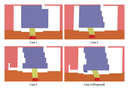
Figure 3 illustrates the simulated evolution of the antenna’s S11 parameter. It can be observed that as the antenna evolves, the bandwidth gradually expands. Furthermore, with the addition of the stub, the antenna’s bandwidth significantly widens, effectively covering the 3.5 GHz (3.3–3.6 GHz) and 4.9 GHz (4.8–5 GHz) frequency bands.
3.2. Dimension Optimization
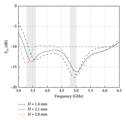
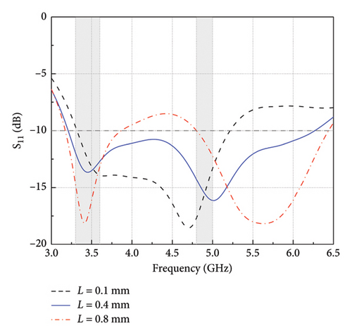
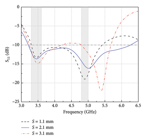
The simulated S11 parameters of the individual antenna element for different values of H, L, and S (as shown in Figure 1) are depicted in Figures 4, 5, and 6, respectively. Adjusting the value of H can influence the resonance frequency of the lower frequency bands and the overall antenna performance. In Figure 4, as H increases, the resonant frequency of the second operating frequency band shifts slightly, while the resonant point in the first operating frequency band shifts to the left. The final value of H is chosen to be 2.1 mm. The value of L can effectively alter the resonance frequency of the higher frequency band. In Figure 5, little resonant frequency offset of the first band arises with the increase in L, while the resonant frequency of the latter shifts significantly. The final value of L is 0.4 mm. Additionally, the value of S simultaneously influences both the resonance depth and the bandwidth, with a more pronounced effect on the latter frequency band. The optimal value for S is 2.1mm. Ultimately, these adjustments enable the antenna to operate within the frequency range of 3.4–3.6 GHz and 4.8–5 GHz. When L = 0.4 mm, H = 2.1 mm, and S = 2.1 mm, the desired frequency bands can be well covered.
3.3. Isolation Optimization
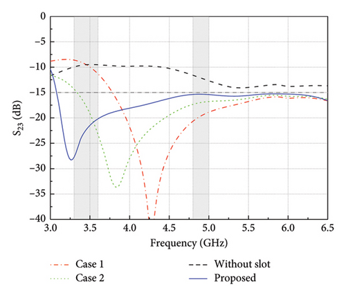
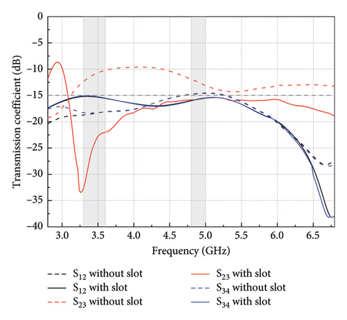
Since the eight antenna elements are arranged in pairs vertically at the four corners of the system circuit board, they minimize the mutual coupling caused by their proximity to the greatest extent. This arrangement results in excellent isolation between Ant. 1 and Ant. 2, Ant. 3 and Ant. 4, Ant. 5 and Ant. 6, as well as Ant. 7 and Ant. 8. As a result, the isolation between only Ant. 2 and Ant. 3, as well as between Ant. 6 and Ant. 7, poses a significant challenge. Based on the DGS, isolation structures are proposed to obtain better isolation performance. Figure 7 illustrates the simulated evolution of these isolation structures. Due to the symmetrical structure of the antennas, for the sake of brevity, this article will focus on the isolation treatment between Ant. 2 and Ant. 3 as a representative case. The simulated S23 of the presented antenna with or without the structure reducing the interaction are presented in Figure 8, which demonstrates that the structure of a dumbbell-shaped slot can increase isolation between Ant. 2 and Ant. 3, as well as Ant. 6 and Ant. 7. The surface current is restrained and its direction is changed by the dumbbell-shaped slot on both sides. Meanwhile, the groove shifts the resonance point of the antenna to the left, allowing the isolation exceeding 15dB to well cover all the designed frequency bands. Without the dumbbell-shaped slots, the port impedance matching conditions are not ideal, resulting in Ant. 2 and Ant. 3 exhibiting isolation performance of only around 10 dB within the operating frequency band. By introducing the dumbbell-shaped slots on the ground plane, significant improvements in port impedance matching conditions are achieved. As shown in Figure 9, within the operating frequency band, the isolation between Ant. 2 and Ant. 3 is notably enhanced. Additionally, positive effects are observed between Ant. 1 and Ant. 2, as well as between Ant. 3 and Ant. 4. These enhancements lead to an overall antenna isolation level larger than 15 dB.
3.4. Current Distribution and 3D Radiation Patterns
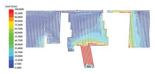
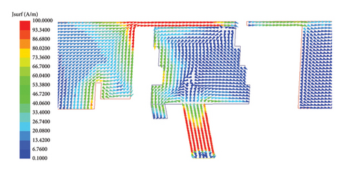
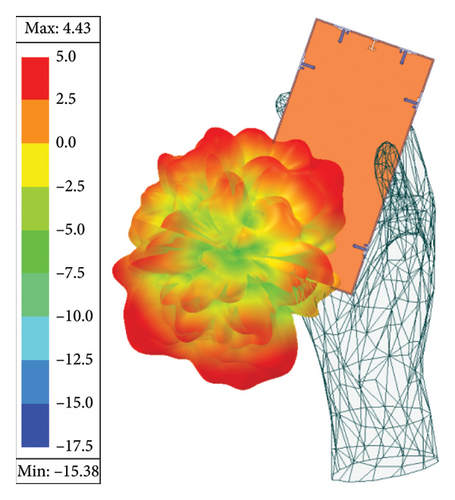
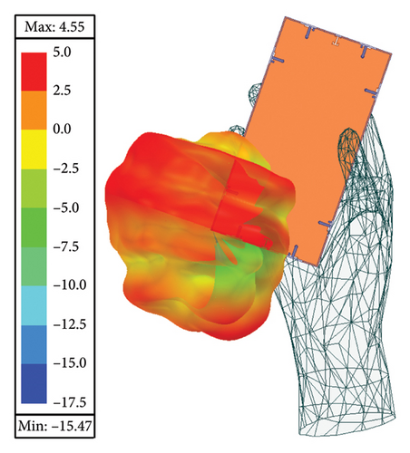
Figure 10 shows the simulated surface current distribution at 3.5 GHz and 4.9 GHz. At 3.5 GHz, the surface current is primarily concentrated on the right side of the frame. Conversely, at 4.9 GHz, it is focused on the left and top sides of the frame. Figure 11 displays the simulated 3D radiation patterns when the device is held in a single hand. The maximum gains are 4.43 dBi at 3.5 GHz and 4.55 dBi at 4.9 GHz, respectively, meeting the requirements for most mobile phone antennas.
4. Experimental Analysis
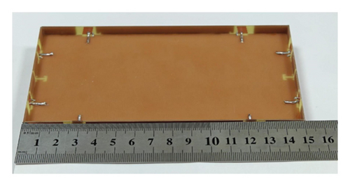
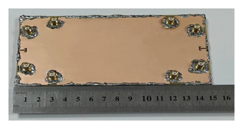
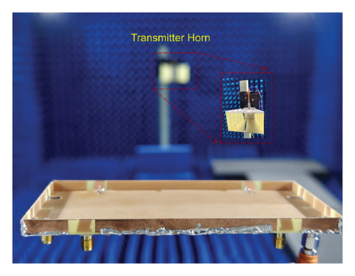
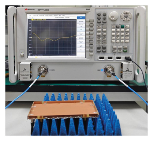
The proposed antenna prototype was printed and measured to validate the simulation results. Figure 12 illustrates the setup using an anechoic chamber testing environment and photographs of the antenna prototype. Figures 12(a) and 12(b) present the top and bottom view of the fabricated antenna prototype. Figure 12(c) shows the measurement environment for the two-dimensional radiation pattern. The vector network analyzer (VNA) used to measure the proposed antenna’s S-parameters is shown in Figure 12(d).
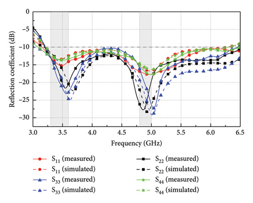
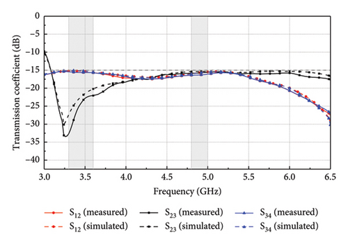
Due to the symmetry of the eight antenna elements about the centerline of the circuit board, the performance of Ant. 5–8 is essentially identical to that of Ant. 1–4. Therefore, discussing the simulation and test results for Ant. 1–4 is sufficient to represent the overall performance of the antenna, which is primarily characterized by the parameters S11, S22, S33, and S44. Additionally, the isolation performance is evaluated using the parameters S12, S23, and S34. Figures 13 (a) and 13(b) compare simulated S-parameters with measured S-parameters (denoted as Sii and Sij, respectively). Minor frequency shifts exist between simulated and measured results, primarily due to the skin effect caused by excess solder. However, the measured results still adequately cover the target frequency bands. It is observed that all antenna elements exhibit reflection coefficients of less than −10 dB and transmission coefficients of less than −15 dB within the operating frequency range of 3.23–6.45 GHz, thereby demonstrating excellent impedance matching and isolation characteristics.
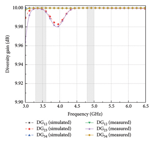
The ECC and DG of the MIMO antenna system are depicted in Figure 14. Within the operational frequency band, the ECC values are less than 0.006, with the minimum value being as low as 0.001, all of which are much lower than the typical carrier requirement of 0.5. The DG values exceed 9.98 dB.

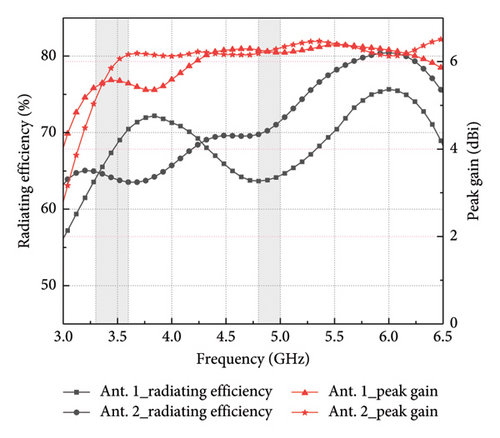
Due to the antenna’s symmetric design, Ant. 1 and Ant. 2 were chosen as representatives for efficiency measurements. Figure 15 illustrates the total efficiency exceeding 60% within the operating frequency band, with a peak gain superior to 5.1 dBi.
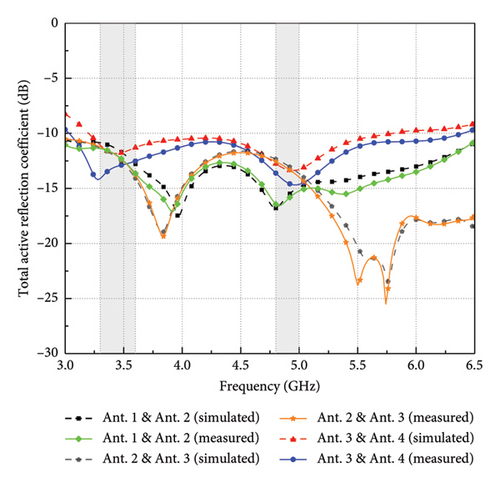
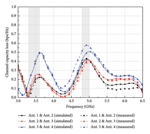
CCL indicates the rate of information transmitted within a communication channel without data loss. The values of CCL can be calculated using equations (4)–(6) [10]:
The computed values of CCL for the presented antenna are displayed in Figure 17(a), showing values smaller than 0.55 within the 3.23–6.45 GHz range, indicating that the CCL of the antenna system designed in this paper is low.
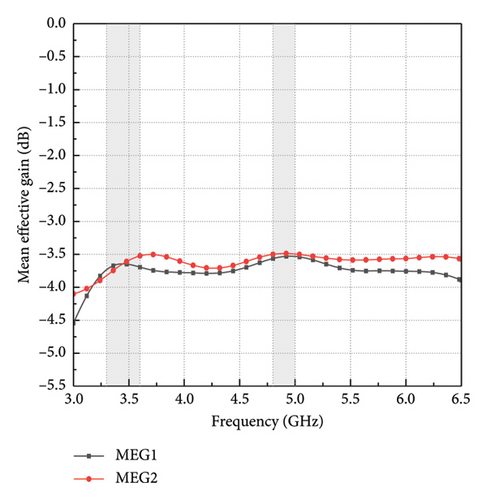
The calculated MEG value for the indicated antenna, as depicted in Figure 17(b), is less than −3.5 dB within the frequency range of 3.23 GHz–6.45 GHz, indicating excellent adaptability to the scattering environment.
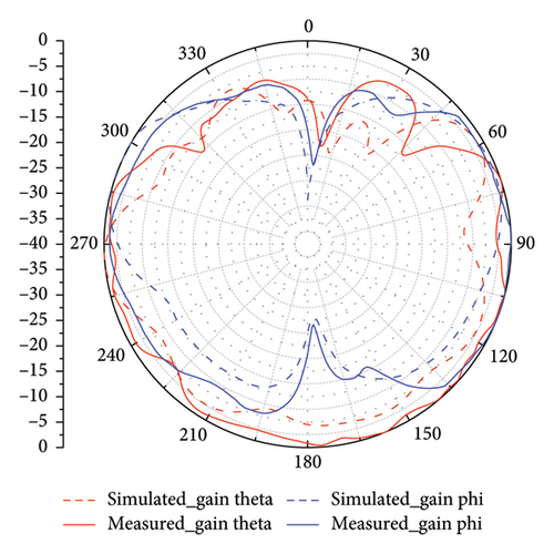
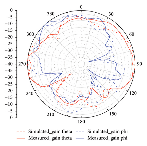
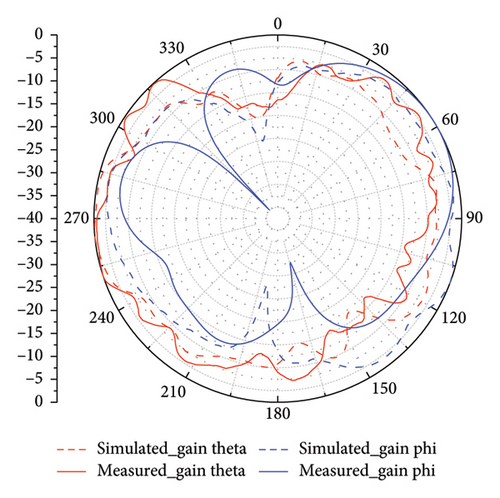
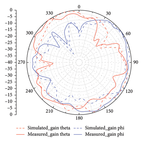
The radiation patterns of the proposed MIMO system at 3.5 GHz and 4.9 GHz are depicted in Figure 18. The measured co-polarization and cross-polarization values are represented by solid lines, while the simulated values are depicted by dashed lines.
As shown in Table 1, compared to other report antennas, the proposed antenna exhibits higher isolation, lower ECC, and a smaller antenna element size.
| Ref. | Operating bands (GHz) | Isolation (dB) | Efficiency (%) | ECC | Element size (mm3) |
|---|---|---|---|---|---|
| [17] | 3.3–5.95 | > 15 | 47–78 | < 0.11 | 17 × 6 × 0.8 |
| [20] |
|
> 13 | > 70 | < 0.1 | 6.5 × 7 × 0.8 |
| [22] | 3.3–6 | > 15 | > 95 | < 0.05 | 24 × 36 × 1.6 |
| [23] |
|
> 11 |
|
< 0.01 | 20.5 × 6.5 × 0.8 |
| [24] | 3.6–3.8 and 5.15–5.92 | > 15 | > 54 | < 0.05 | 18 × 18 × 0.8 |
| [25] | 3.3–6 | > 10 | 40–70 | < 0.1 | 13.9 × 7 × 0.8 |
| [26] | 3.3–5 | > 12 | 31.6–88.6 | < 0.11 | 40 × 3 × 7.5 |
| [27] | 3.3–7.1 | > 12 | 48–89 | < 0.07 | 22 × 22 × 1.6 |
| [28] | 3.3–6 | > 12 | 50–61 | < 0.2 | 22 × 2 × 1 |
| This work | 3.23–6.45 | > 15 | 63–82 | < 0.006 | 6.95 × 6.2 × 0.8 |
5. Conclusion
The paper introduces a broadband eight-element antenna array covering 3.23–6.45 GHz. Each antenna element consists of a stepped radiator and stub. The design evolution and dimensional optimization of the single antenna element are analyzed to enhance performance. The innovative aspect of this work lies in the compact size of the individual antenna elements, measuring only 6.95 mm × 6.2 mm. Experimental total efficiency exceeds 60%, with values higher than 75% within the frequency ranges of 3.4–3.6 GHz and 4.8–5 GHz. Its isolation is superior to 15 dB, accompanied by a very low ECC. The antenna is validated through simulation and measurement. The proposed antenna offers comprehensive performance advantages in its compact size, making it a promising candidate for 5G smartphones [29].
Disclosure
All of the figures, materials, and data within the manuscript are original and owned by authors.
Conflicts of Interest
The authors declare no conflicts of interest.
Author Contributions
Conceptualization, W.L., and L.H.; methodology, L.H. and S.X.; data curation, W.L. and S.X.; investigation, W.L., and L.H.; writing – original draft preparation, W.L.; writing – review and editing, G.L.; supervision and funding acquisition, G.L. All authors have read and agreed to the published version of the manuscript.
Funding
This research was supported by National Natural Science Foundation of China (10.13039/501100001809) ∗ 61671330, Science and Technology Department of Zhejiang Province (10.13039/501100008990) ∗ LGG19F010009, and Wenzhou Municipal Science and Technology Program ∗ C20170005 ∗ 2018ZG019.
Acknowledgments
This work was funded in part by the National Natural Science Foundation of China under Grant No. 61671330, the Science and Technology Department of Zhejiang Province under Grant No. LGG19F010009, and Wenzhou Municipal Science and Technology Program under Grant No. 2018ZG019.
Open Research
Data Availability Statement
All data generated or analyzed during this study are included within this article.


