Volume 2025, Issue 1 5033174
Research Article
Open Access

Wideband Compact Planar Antenna With Curved Transmission Lines and ACPW Structure

Mohamed Elhefnawy

Mohamed Elhefnawy

Department of Electronic Engineering , Gyeongsang National University (GNU) , B405-401 501 Jinju-Daero, Jinju , 52828 , Gyeongnam, Republic of Korea , gnu.ac.kr

Department of Electrical Engineering , Faculty of Engineering , October 6 University , 6th of October City , Egypt , o6u.edu.eg

Search for more papers by this author
Kyoung-Hun Kim

Kyoung-Hun Kim

Department of Electronic Engineering , Gyeongsang National University (GNU) , B405-401 501 Jinju-Daero, Jinju , 52828 , Gyeongnam, Republic of Korea , gnu.ac.kr

Search for more papers by this author
Wang-Sang Lee

Corresponding Author

Wang-Sang Lee

Department of Electronic Engineering , Gyeongsang National University (GNU) , B405-401 501 Jinju-Daero, Jinju , 52828 , Gyeongnam, Republic of Korea , gnu.ac.kr

Search for more papers by this author
First published: 23 July 2025
Academic Editor: Mohammad Hassan Neshati

Abstract

In this paper, the proposed wideband compact planar antenna is realized by incorporating multiple curved transmission lines along with the interdigital capacitor (IDC) and the electric inductor–capacitor (ELC) resonator. Furthermore, this antenna implements an asymmetric coplanar waveguide (ACPW) via-less structure. A prototype of the proposed antenna has been fabricated with a compact size of 0.33λ0 × 0.26λ0 at the lower operating frequency of 2.3 GHz. The obtained measured results indicate a wide bandwidth that can cover the frequency band from 2.3 GHz to 4.11 GHz, corresponding to a −10 dB fractional bandwidth of 56.47%.

1. Introduction

There has been significant interest in wideband and compact planar antennas. Planar antennas, in various configurations, offer attractive features such as being low-profile, lightweight, and having a wide bandwidth. Nevertheless, designing these antennas becomes more challenging as the need arises to decrease their size while expanding the operating frequency band. Consequently, numerous efforts have been made to enhance the bandwidth and miniaturize planar antennas. For instance, a triple-band slotted bow-tie antenna with curved monopoles was discussed in [1]. The authors of [2] presented an antenna capable of covering GSM and Wi-Fi/WLAN frequencies using a rectangular patch and a high-impedance microstrip line. Additionally, a compact and broadband antenna featuring a Y-shaped central monopole was investigated in [3]. In [4], a CPW-fed monopole antenna with a parasitic circular-hat patch and slotted CPW ground was developed to excite dual resonant modes and enhance the overall impedance bandwidth. Moreover, a compact bow-tie quasi-self-complementary antenna suitable for ultrawideband (UWB) applications was proposed in [5]. The authors of [6] introduced a dual-band magnetoelectric dipole antenna with complementary capacitively loaded loop slots, while the authors of [7] presented a compact coplanar-fed planar multiband antenna. In [8], two composite right-/left-handed transmission line (CRLH-TL) unit cells are integrated with a monopole. These two CRLH-TL structures create two separate zeroth-order resonances (ZORs). By adjusting the length of the meander line in each CRLH-TL unit cell, these two resonant modes can be combined to expand the lower bandwidth from 820 to 960 MHz. Additionally, the quarter-wavelength monopole generates a resonant mode in the DCS1800/PCS1900/UMTS band.

The development of antennas for wireless energy harvesting represents a critical research area. An essential design parameter, in addition to achieving wide bandwidth and compact size, is the antenna’s ability to detect both copolarization and cross-polarization components of the incident wave, thereby enhancing energy reception. In [9, 10], the antenna exhibits both copolarization and cross-polarization radiated fields, indicating its capability to receive RF waves with vertical or horizontal polarization. This performance validates the antenna’s effectiveness for use in wireless energy harvesting applications. In [11], the average received power was measured in urban areas, ant it was found that the combined reception of cross-polarized waves significantly enhances the received power.

This paper introduces an antenna design that incorporates curved segments of transmission lines, an IDC, and an ELC resonator. The proposed antenna features a via-less, single-layer geometry with enhanced bandwidth, achieved through the utilization of an asymmetric coplanar waveguide (ACPW) structure. The use of the IDC helps to increase the overall capacitance of the proposed antenna. Furthermore, curved transmission line sections have been implemented to achieve higher inductance values in a smaller area. The incorporation of the IDC, ELC, and curved segments of transmission lines provides the flexibility to manipulate both the total inductance and capacitance of the proposed antenna. This manipulation allows for an increase in the overall capacitance and inductance within the structure, leading to a downward shift in the resonance frequency and consequently reducing the physical dimensions of the antenna relative to its operating wavelength. The design choice for the curved segments of the transmission lines also enables the reception of both copolarization and cross-polarization components of the incident wave. Furthermore, the ELC resonator enhances the antenna’s ability to achieve high absorptivity. The proposed antenna was designed as a promising choice for wireless energy harvesting applications.

2. Development of the Proposed Antenna
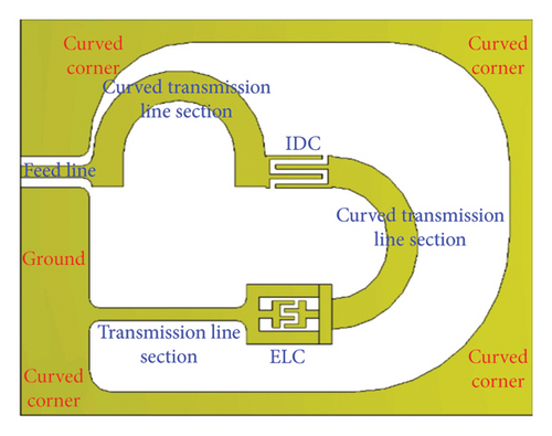
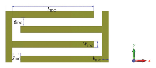
The structure of the proposed antenna consists of a feed line section connected to a curved transmission line section and an IDC. Additionally, there is another curved transmission line that connects the IDC to the ELC resonator. The ELC resonator is then connected to the ground through a transmission line section, as shown in Figure 1(a). The IDC can be used to realize capacitance values of less than 1 pF. The series capacitance of the IDC is highly dependent on the number of fingers and the spacing between them, and it increases proportionally with the length of the fingers. The microstrip structure for the IDC, as shown in Figure 1(b), can be converted into lumped capacitance. The following approximate closed-form expression is used to calculate the IDC capacitance in pF [12]:
()
Details are in the caption following the image
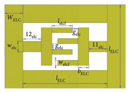
Geometry of the proposed antenna: (a) components of the proposed antenna, (b) microstrip structure for the IDC (LIDC = 4.5 mm, WIDC = 0.36 mm, gIDC = 0.46 mm, and bIDC = 0.36 mm), (c) microstrip structure for the ELC resonator (lELC = 5.1 mm, WELC = 1.11 mm, welc = 0.66 mm, lelcf = 1.25 mm, welcf = 0.31 mm, gelc = 0.35 mm, bELC = 0.66 mm, l1elc = 1.12 mm, and l2elc = 1.11 mm), (d) dimensions of the proposed antenna (W = 34.1 mm, L = 44.1 mm, Lr = 10.3 mm, L1 = 8.9 mm, W1 = 11.8 mm, Wc = 9 mm, C1 = 4.45 mm, qr = 9.7 mm, qt = 2.6 mm, Wb = 6.3 mm, Ld = 13.5 mm, Cd = 6.74 mm, Cr = 5.17 mm, Cdl = 0.94 mm, lf = 6.2 mm, Ldl = 1.9 mm, Wd = 19.9 mm, Wf = 1 mm, Cc = 0.85 mm, and Wk = 1.1 mm).
In (1), N represents the number of fingers and LIDC represents the length of the IDC finger. The IDC effective dielectric constant εeff can be determined as follows:
()
The substrate thickness is denoted as h, and bIDC represents the width of the IDC edge. Additionally, the dielectric constant of the substrate is denoted as εr. The elliptic functions K(k) and K(k) are mathematically defined as follows [12]:
()
()
()
The IDC finger’s width is represented by WIDC, and the space between the IDC fingers is represented by gIDC.
()
The ELC resonator consists of a capacitor connected in parallel to two inductive loops [13]. The first step in the ELC design process involves converting the microstrip structure into equivalent lumped elements using empirical equations. The dimensions of the ELC resonator, as depicted in Figure 1(c), are used to calculate the value of the lumped inductance equivalent to the two outer inductive loops and the center branch. Each outer loop has a total length of 2lELC, and its inductance LELC is calculated using the following closed-form formula [12]:
()
The strip thickness is denoted as t, while the conductor width is represented by WELC. kg represents the correction factor of the strip which can be expressed by
()

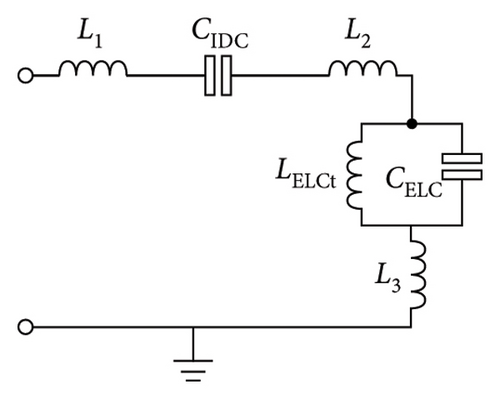
The inductance value for the ELC central branch (LCN) can be determined by using (7), where the total length of the central conductor is represented by (l1elc + l2elc) and its width is denoted by welc. The total inductance of the ELC resonator is obtained as LELCt = (LELC/2)‖LCN. Moreover, Figure 1(c) depicts the dimensions of the microstrip structure of the interdigital capacitor within the ELC resonator, which can be substituted into (1), to determine the lumped value of the IDC capacitance (CELC) in the ELC resonator. Furthermore, the inductance values (L1) and (L2) of each curved transmission line section can be determined by replacing the width and length parameters in (7) with the corresponding dimensions of each curved transmission line section, as depicted in Figure 1(d). In addition, the transmission line segment that connects the ELC resonator to the ground has an inductance denoted as (L3). The determination of this inductance value is achieved through (7) by replacing the conductor’s length and width with (Ld) and (Wk), respectively. The lowest resonance frequency of the proposed antenna depends on the dimensions of the transmission line sections, as well as the configurations of the IDC and the ELC resonator. This resonance frequency can be calculated as , where Ltot and Ctot represent the total inductance and capacitance of the proposed antenna, as indicated in Figure 2.
Details are in the caption following the image
Simplified equivalent circuit model for the proposed antenna.

3. Results and Discussions

The proposed antenna was simulated and fabricated on the FR4 substrate with a thickness of 1 mm and a dielectric constant of 4.4. The design process began by developing a CST model. Subsequently, the tuning and optimization tools available in CST Studio Suite were utilized to enhance the CST simulation results. The optimized dimensions for the proposed antenna are illustrated in Figures 1(b), 1(c), and 1(d). The via-free single-layer antenna was constructed by implementing the ACPW structure.

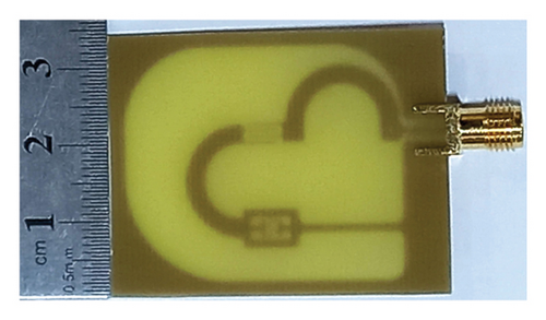
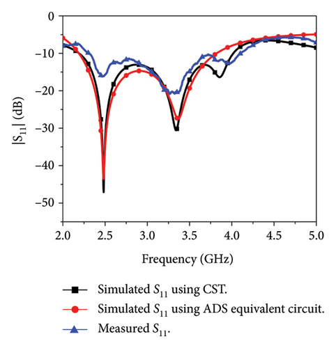
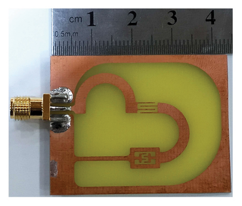
A prototype of the antenna was fabricated, as shown in Figure 3. The reflection coefficients, both simulated and measured, are plotted in Figure 4. The Rohde & Schwarz ZNB 40 vector network analyzer was used to measure the S-parameters. The measured −10 dB bandwidth ranges from 2.3 GHz to 4.11 GHz, with a fractional bandwidth (FBW) of 56.47%.
Details are in the caption following the image
Fabricated prototype of the proposed antenna: (a) top view and (b) bottom view.
Details are in the caption following the image
Fabricated prototype of the proposed antenna: (a) top view and (b) bottom view.
Details are in the caption following the image
S-parameters for the proposed antenna.

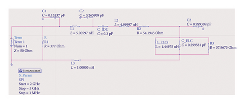
The equivalent circuit model of the proposed antenna was developed by first calculating the inductances L1, L2, LELCt, and L3 using (7)–(8), which initially resulted in values of 3.16, 2.68, 0.35, and 2.7 nH, respectively. Similarly, the capacitances CIDC and CELC were initially determined based on (1)–(6), with initial values of 0.36 and 0.11 pF. The coupling between the feed line and ground was accounted for by incorporating the coupling capacitance C1, while the coupling capacitances between the curved transmission line sections and the ground were modeled by adding C2 and C3 to the equivalent circuit. Moreover, the radiation resistances associated with the transmission line segments and the ELC resonator were represented as R2 and R3, respectively. Finally, the free-space characteristic impedance R1 was connected in parallel with the proposed antenna’s equivalent circuit. The complete equivalent circuit model was simulated using ADS software, as illustrated in Figure 5. The component values in the circuit model were optimized and fine-tuned to achieve an S-parameter closely matching that obtained from CST simulations, as shown in Figure 4.
Details are in the caption following the image
Equivalent circuit model of the proposed antenna using ADS.

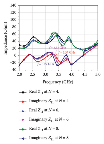
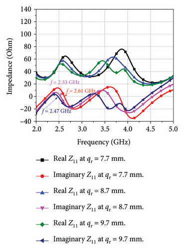
A parameter analysis was conducted to examine the impact of variations in structural dimensions on the performance of the proposed antenna. Specifically, the effects of modifying the dimensions of the curved transmission lines and the number of IDC fingers on the resonance frequencies were analyzed while maintaining the overall size of the proposed antenna at 0.33λ0 × 0.26λ0. Figure 6(a) shows that increasing the diameter of the curved transmission line from 7.7 mm to 9.7 mm shifts the lowest resonant frequency downward from 2.61 GHz to 2.47 GHz. Additionally, as shown in Figure 6(b), increasing the number of IDC fingers from 4 to 8 results in a resonant frequency shift from 3.37 GHz to 3.27 GHz.
Details are in the caption following the image
Effect of variations in structural dimensions on the Z-parameters of the proposed antenna. (a) Influence of curved transmission line dimensions. (b) Effect of varying the number of IDC fingers.
Details are in the caption following the image
Effect of variations in structural dimensions on the Z-parameters of the proposed antenna. (a) Influence of curved transmission line dimensions. (b) Effect of varying the number of IDC fingers.

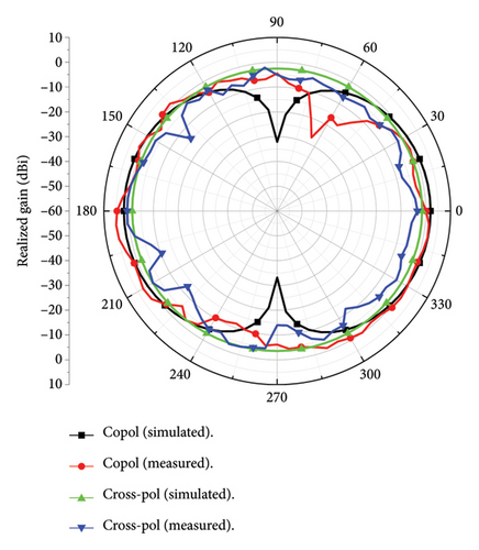
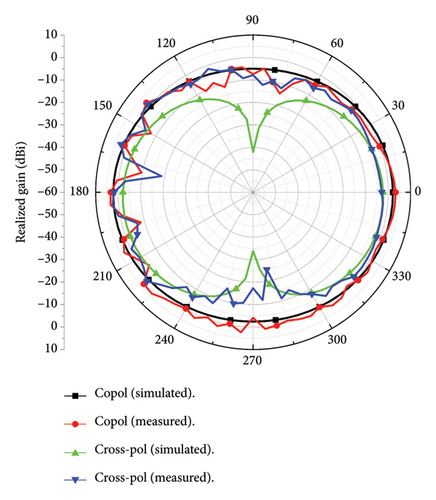
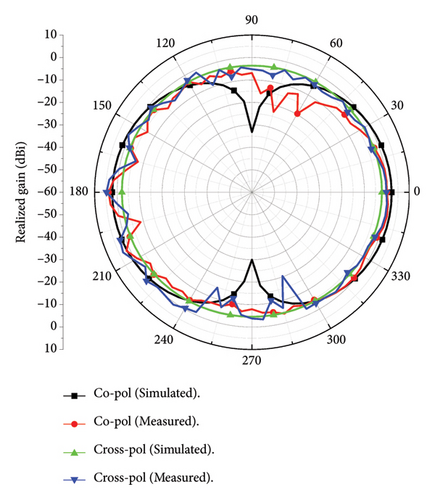
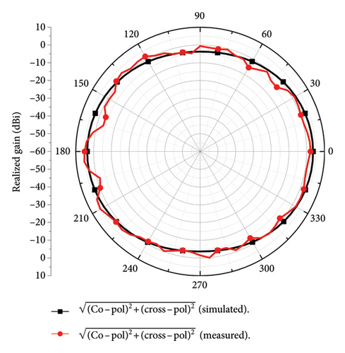
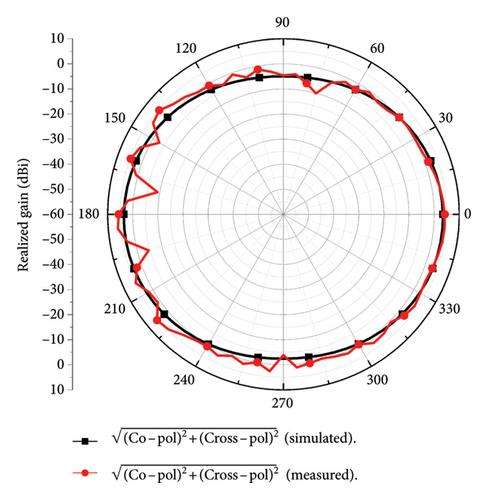
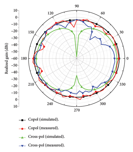
The simulated and measured far-field realized gain at frequencies of 2.5 GHz and 3 GHz is depicted in Figure 7. These patterns exhibit a nearly omnidirectional characteristic across all frequencies of interest. Additionally, the far-field realized gain observed in the xz and yz planes is almost identical. Figures 7(a) and 7(d) further illustrate that both copolarization and cross-polarization components can be received. Figures 7(e), 7(f), 7(g), and 7(h) show the total radiation patterns of XY and YZ planes at 2.5 and 3 GHz, respectively.
Details are in the caption following the image
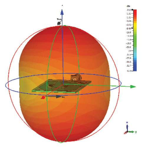
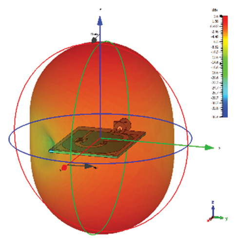
Simulated and measured far-field realized gains of the proposed antenna: (a) copol and cross-pol at 2.5 GHz: XZ plane, (b) copol and cross-pol at 2.5 GHz: YZ plane, (c) copol and cross-pol at 3 GHz: XZ plane, (d) copol and cross-pol at 3 GHz: YZ plane, (e) total radiation pattern at 2.5 GHz: XZ plane, (f) total radiation pattern 2.5 GHz: YZ plane, (g) total radiation pattern 3 GHz: XZ plane, (h) total radiation pattern 3 GHz: YZ plane, (i) simulated 3D far-field realized gain at 2.5 GHz, (j) simulated 3D far-field realized gain at 3 GHz.

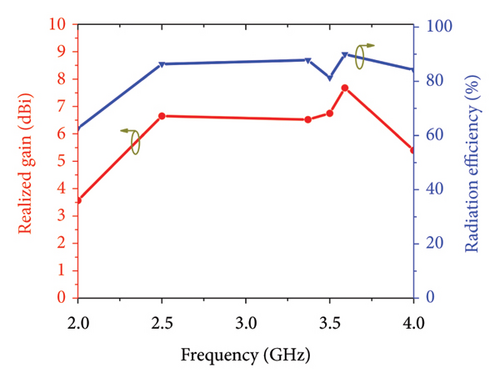
The radiation characteristics of the proposed antenna were measured at the Korea Institute of Electronic Technology. In the frequency band of 2–5 GHz, the maximum measured total efficiency (η) is 89.96%, while the measured antenna’s peak realized gain is 7.68 dBi as shown in Figure 8.
Details are in the caption following the image
Realized gain and radiation efficiency of the proposed antenna.

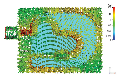
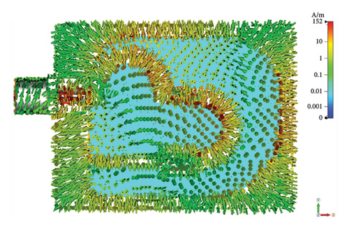
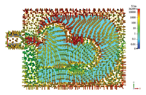
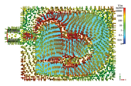
Figures 9(a) and 9(b) illustrate that the electric field distribution is more intense near the transmission line sections, IDC, and the ELC resonator, which causes the operating frequency of the proposed antenna to be determined by the geometry of these components. Moreover, the geometry of the curved sections allows the proposed antenna to support diverse polarizations. As illustrated in Figures 9(c) and 9(d), the electric and magnetic field lines are perpendicular to one another, resulting in omnidirectional radiation, as indicated in Figures 7(i) and 7(j).
Details are in the caption following the image
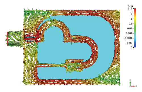
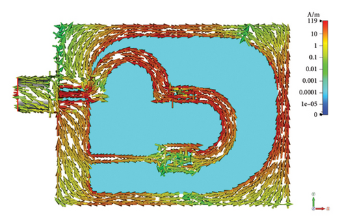
CST simulation of the electric field, magnetic field, and surface current distributions at multiple frequencies. (a) Electric field distribution at 2.5 GHz. (b) Electric field distribution at 3.37 GHz. (c) Magnetic field distribution at 2.5 GHz. (d) Magnetic field distribution at 3.37 GHz. (e) Surface current distribution at 2.5 GHz. (f) Surface current distribution at 3.37 GHz.

The surface current distribution on the curved sections of the transmission line, IDC, and the ELC resonator induces an additional surface current distribution on the ground plane of the proposed ACPW antenna, as illustrated in Figures 9(e) and 9(f). This phenomenon increases the effective radiating area, enhances radiation efficiency, and contributes to improved bandwidth and gain performance.

Table 1 compares the proposed antenna with previously published relevant studies. The proposed antenna exhibits a significantly wide bandwidth, a relatively compact size of 0.33λ0 × 0.26λ0, and a via-free, single-layer simple structure that can achieve high performance without the need for varactors or pin diodes. Although some designs, such as [15], feature a smaller footprint, they achieve this at the cost of reduced bandwidth and lower gain. Additionally, certain compact designs introduce structural complexities, such as the use of vias in [14, 18, 19], or varactors in [16, 17]. The designs in [20, 21] also provide wideband operation with FBWs of 51.6% and 61%, respectively. However, their peak gains (3.7 dBi and 3.8 dBi) are significantly lower than that of the proposed antenna.

Table 1. Comparison of the proposed antenna with previously published studies.
Ref. Dimensions (λ0 × λ0) No. of metal layers No. of vias No. of diodes BW (GHz) FBW (%) Max. Eff. (%) Peak gain (dBi)
[9] 0.42 × 0.42 2 No No 1.8–2.5 32.56 NA 4.1
  
[10] 0.35 × 0.32 1 No No 0.85–1.94 78.14 75 2
  
[14] 0.21 × 0.08 2 2 No 2.41–2.43 1 53 −0.53
  
[15] 0.12 × 0.13 1 No No 1.56–1.64 5 88 2.9
3.43–3.65 6.21
4.2–7.59 57.2
  
[16] 0.18 × 0.16 2 No 3 varactors 1.58–2.12 29.1 < 40 4
2.24–2.68 17.8
3.08–3.78 20.4
  
[17] 0.11 × 0.1 2 No 1 varactor 0.75–0.96 24.5 78 2.1
1.25–1.94 43.2
  
[18] 0.19 × 0.09 2 3 No 2.85–2.9 1.7 46 −0.82
  
[19] 0.2 × 0.14 2 2 No 2.25–2.35 4.4 79 2.3
  
[20] 0.39 × 0.33 1 No No 2.3–3.9 51.6 NA 3.7
  
[21] 0.24 × 0.49 1 No No 2.8–5.25 61 NA 3.8
  
This work 0.33 × 0.26 1 No No 2.3–4.11 56.47 89.96 7.68

The proposed antenna can be a promising choice for wireless energy harvesting applications within the 2.3–4.11 GHz range, particularly for IoT devices and low-power sensors. This frequency range overlaps with ambient RF sources such as Wi-Fi (2.4 GHz) and LTE bands, enabling efficient energy capture.

4. Conclusion

This paper introduces a novel antenna design utilizing an ACPW structure with curved transmission line segments, an IDC, and an ELC resonator. Incorporating the IDC, ELC, and curved transmission line sections results in a lower resonance frequency and a reduction in physical dimensions relative to the antenna’s operating wavelength. The proposed antenna, with an ACPW structure, exhibits a wide bandwidth and a compact physical size of 0.33λ0 × 0.26λ0. Experimental measurements demonstrate that the antenna achieves an impedance bandwidth of −10 dB, spanning 1.81 GHz (2.3–4.11 GHz). Furthermore, the proposed antenna design features a simple structure without vias, a nearly omnidirectional radiation pattern, and the ability to receive both copolarization and cross-polarization waves. Therefore, the proposed antenna can be a promising choice for wireless energy harvesting applications.

Conflicts of Interest

The authors declare no conflicts of interest.

Funding

This work was supported in part by the Korean Government (MSIT) through the National Research Foundation of Korea, South Korea, under Grant RS-2024-00338277 and in part by the Institute of Information & Communications Technology Planning & Evaluation (IITP) grant funded by the Korea government (MSIT), under Grant RS-2022-00156409 (ICT innovation human resources 4.0).

Data Availability Statement

Data sharing is not applicable to this article as no datasets were generated or analyzed during the current study.

    The full text of this article hosted at iucr.org is unavailable due to technical difficulties.