Volume 2025, Issue 1 9966942
Research Article
Open Access

Controlled Growth Temperatures of High Dielectric Constant Gallium Cerium Oxide Layer on 4H-Silicon Carbide Substrate

Abdul Shekkeer Kammutty Musliyarakath

Abdul Shekkeer Kammutty Musliyarakath

Institute of Nano Optoelectronics Research and Technology (INOR) , Universiti Sains Malaysia , Penang , 11800 , Malaysia , usm.my

Search for more papers by this author
Kuan Yew Cheong

Kuan Yew Cheong

School of Materials and Mineral Resources Engineering , Universiti Sains Malaysia , Nibong Tebal , 14300 , Penang , Malaysia , usm.my

Search for more papers by this author
Hock Jin Quah

Corresponding Author

Hock Jin Quah

Institute of Nano Optoelectronics Research and Technology (INOR) , Universiti Sains Malaysia , Penang , 11800 , Malaysia , usm.my

Search for more papers by this author
First published: 05 May 2025
Academic Editor: Rami Reddy Boppella

Abstract

The potential of using gallium cerium oxide (GaxCeyOz) as a passivation layer (PL) on 4H-silicon carbide (SiC) substrates were thoroughly assessed after annealing in nitrogen–oxygen–nitrogen (N2–O2–N2) ambient at varying temperatures of 600, 700, 800, and 900°C. It was observed that nitrogen ions introduced during the annealing process were predominantly attached to oxygen vacancies (Vo) within the oxide layer at lower temperatures (600 and 700°C), whereas at elevated temperatures (800 and 900°C), there was a substantial increase in the migration of nitrogen ions toward the interface of GaxCeyOz/4H-SiC. Analysis employing X-ray photoelectron spectroscopy (XPS) corroborated the transformation of Ce3+ to Ce4+ at 900°C due to enhanced reoxidation. As a result, the passivation of Vo at 800 and 900°C led to a significantly higher dielectric constant, improved breakdown field, and favorable values for slow trap density (STD), interface trap density, interface state density, as well as effective oxide charge, highlighting the potential of GaxCeyOz PL on 4H-SiC for use in metal–oxide–semiconductor (MOS) applications.

1. Introduction

In the pursuit of energy-efficient technologies to achieve sustainable solutions for the next generation of power electronic devices, various approaches utilizing wide bandgap semiconductor materials have been successfully adopted in the development of these power electronic devices. It was anticipated that wide bandgap semiconductors, especially 4H-silicon carbide (SiC), has emerged as the choice of semiconductor substrate for metal–oxide–semiconductor (MOS) devices that would provide excellent performance in meeting the future market demands of power electronic devices requiring high energy efficient, effective in heat dissipation, high switching frequency, and ability to operate at high temperatures [1]. The 4H-SiC was experiencing a profound exploration for high temperature as well as high power device applications owing to the possession of wide energy bandgap (3.26 eV), high saturation drift velocity (2.7 × 107 cm/s), high thermal conductivity (~4.9 W cm−1 K−1), as well as high critical electrical field (~3 MV/cm) [2]. The possession of both wide energy bandgaps coupled with high thermal conductivity by 4H-SiC would allow the 4H-SiC-based MOS devices to operate reliably at high temperatures (>250°C) due to effective heat dissipation while Si-based MOS devices have displayed degradation in performance at this range of operating temperature [35]. Additionally, 4H-SiC-based MOS devices were able to achieve high-frequency switching capability due to the lower impurity concentration of 4H-SiC substrate that allowed this semiconductor material to attain high saturation velocity and mobility [6, 7]. Another potential appeal of using 4H-SiC as the semiconductor substrate was the ability to adopt the matured fabrication and packaging technologies developed for Si-based MOS devices to be employed in the development of 4H-SiC-based MOS devices [8].

Another captivating advantage of 4H-SiC, when compared with other compound semiconductors, is the ability to thermally grow high-quality native silicon dioxide (SiO2) or nitrided SiO2 as a passivation layer (PL), of which 4H-SiC-based MOS devices with nitrided SiO2 has demonstrated low leakage current, as well as leveraging on the well-established fabrication process from Si-based MOS devices [9, 10]. Nevertheless, a challenge arose when using low dielectric constant (k) SiO2 for the passivation for 4H-SiC-based MOS devices due to the breakdown of the device being caused by the low k value of SiO2, hindering the complete exploitation of the high breakdown field strength possessed by 4H-SiC substrate [11]. Therefore, the alternative method of introducing high k material to be employed as a PL for 4H-SiC-based MOS devices has been carried out in full swing to address this issue, of which these 4H-SiC-based MOS devices would be able to sustain a high breakdown electric field as well as low leakage current density [7]. Currently, there exists a diverse range of advanced high k materials, including cerium oxide (CeO2) [12], aluminum (Al) oxide (Al2O3) [13], zirconium oxide (ZrO2) [14], and lanthanum oxide (La2O3) [15], which have been under consideration as potential substitutes for SiO2 in the role of PL for MOS devices based on 4H-SiC [16]. Among the high k materials under scrutiny, CeO2 stands out as a promising contender for supplanting SiO2 as a PL, thanks to its appealing attributes of values of high k spanning from 10 to 16 [17, 18], wide bandgap spanning from 3.0 to 3.6 eV [17, 19], as well as large conduction band offset with respect to 4H-SiC substrate (1.60 eV) [20]. Likewise, the primary utilization of CeO2 as a PL on Si-based MOS devices has shown a leakage current density reduction, leading to an enhancement in the electric breakdown field [21]. In order to emulate the success of Si-based MOS device with CeO2 as PL, CeO2 has been deposited as PL on 4H-SiC as well as AlGaN/GaN heterostructure, wherein CeO2/4H-SiC MOS test structure has demonstrated a low leakage current density of 1.5 × 10−6 A/cm2 at 3.5 MV/cm as well as low interface trap density (1 × 1012 eV−1 cm−2) [20] while CeO2/AlGaN/GaN MOS test structure has revealed several magnitude reduction of leakage current density when compared with AlGaN/GaN test structure without CeO2 PL [22].

Although CeO2 PL has displayed superior passivating properties, the generation of Vo, in coupled with the reduction of Ce4+ to Ce3+ states, remains as a challenging issue to be tackled [23], wherein the generated Vo has induced gap states triggering the reduction of energy bandgap as well as acting as leakage current paths [24]. Moreover, the generation of oxygen vacancy sites in CeO2 PL would act as a hopping site for the diffusion of oxygen ions to the interface [16], provoking the formation of low k SiO2 and a low passivating quality CeO2 for 4H-SiC [25] and GaN [26] substrates, respectively. In order to tackle these problems and enhance the passivating properties of CeO2, an approach involving the doping of tetravalent cations, which include titanium (IV) (Ti4+) [27], hafnium (IV) (Hf4+), silicon (IV) (Si4+), and zirconium (IV) (Zr4+) [28] into CeO2 crystal lattice has been explored. Unfortunately, this exploration has led to the generation of additional active Vo in CeO2 PL as the doping of these tetravalent cations has stimulated the reducibility of Ce4+ to Ce3+ in which the detrimental effects of Vo have been explained in an earlier section [29]. Therefore, the attention was diverted toward the doping of trivalent cation (yttrium (III) (Y3+) [30], lanthanum (III) (La3+) [31], gadolinium (III) (Gd3+) [32], manganese (III) (Mn3+) [33]) into CeO2 crystal lattice, wherein the reducibility to Ce3+ state was less likely to happen as a lower energy is required for the trivalent cation introduction into CeO2 crystal lattice than the energy required to form oxygen vacancy [34, 35]. While the generation of Vo during the modification CeO2 with trivalent dopant was unavoidable, studies have indicated that these vacancies tend to aggregate into defect clusters along with the trivalent cations, ultimately resulting in the inactivation of the Vo [36] that would retard the oxygen ions from using the Vo as a path to diffuse to interface [37].

Considering these literature reviews, a trivalent Ga3+ cation possessing an ionic radius (0.062 nm), which is smaller in comparison to the Ce4+ cation (0.097 nm), has been introduced into CeO2 crystal lattice with the purpose of enhancing the inactivation of Vo, wherein the probability of forming inactive Vo with trivalent cations was dependent on the ionic radius of trivalent cations [38]. Hence, the introduction of trivalent Ga3+ cation in CeO2 crystal lattice would assist in enhancing the passivating properties of ternary gallium cerium oxide (GaxCeyOz) by taking advantage on the excellent properties of Ga2O3, such as large bandgap (~4.9 eV) and moderate k value (~9) [39, 40]. It is important to note that the prior studies on GaxCeyOz PL were conducted exclusively by the same research group associated with the present work [16, 24, 29]. While earlier research provided a preliminary investigation of Ga3+ doped CeO2 PL on 4 H-SiC, which is the only study on the GaxCeyOz PL deposited on 4H-SiC substrates at 800°C [40], this study represents the first comprehensive analysis of the structural, chemical, optical, and MOS characteristics of GaxCeyOz PL deposited on 4H-SiC substrates. Specifically, examination on the effects of postdeposition annealing at varying temperatures (600, 700, 800, and 900°C) in a nitrogen-oxygen–nitrogen (N2–O2–N2) ambient, offering novel insights into the material’s behavior under these conditions, which has not been reported previously.

2. Experimental

The n-type 4H-SiC (0001) substrate was divided into 1 cm2 sections, cleaned via the RCA process, and immersed in a diluted hydrofluoric acid solution to eliminate the native oxide layer, followed by a rinse with deionized water and drying with nitrogen gas. In the preparation of a gallium precursor with a concentration of 0.25 M, a precise procedure was executed wherein 0.319 g of gallium nitrate hydrate was meticulously dissolved in a volume of 5 ml of methanol, followed by an extensive stirring process conducted at a controlled temperature of 30°C for a duration of 15 min, ensuring the complete dissolution of the compound. Similarly, a cerium precursor of the same molarity, 0.25 M, was synthesized through the dissolution of 1.0936 g of cerium acetylacetonate hydrate in a carefully measured mixture of 3 ml of methanol and 6 ml of acetic acid, which was subsequently subjected to stirring at an elevated temperature of 60°C for an equivalent period of 15 min, thereby facilitating the formation of a homogenous solution. Following the successful preparation of both precursor solutions, the next step involved combining both solutions, which was accompanied by a vigorous stirring process maintained at 60°C for a total of 30 min, thereby ensuring thorough mixing and interaction of the components. Ultimately, the resulting mixture was applied onto a 4H-SiC substrate utilizing a spin-coating technique executed at a speed of 3000 rpm for a precise duration of 30 s, thereby achieving a uniform coating necessary for subsequent experimental procedures. Subsequently, postdeposition annealing was carried out at temperatures between 600 and 900°C in an N2–O2–N2 ambient in a horizontal tube furnace. A gas flow rate of 100 ml/min was chosen in this work, while the heating-up rate was set to 10°C/min.

The crystal structure of the investigated GaxCeyOz PLs was analyzed using grazing incident X-ray diffraction (Bruker D8 Discover employing Cu kα radiation (λ = 1.5406 Å)) operated at 40 kV and 40 mA with a scan range of 25°–62°, a step size of 0.05°, and a step time of 1.5 s. The chemical states of the investigated GaxCeyOz PL were characterized by X-ray photoelectron spectroscopy (XPS) (Axis Ultra DLD Kratos spectrometer) employing a monochromatic Al kα X-ray source (hv = 1486.6 eV) at 9 mA for emission and 10 kV for anode HV (high voltage). Additionally, an analysis area of 300 × 700 µm was utilized to characterize the investigated PL at a base pressure of 2.7 × 10−9 torr under an ultra-vacuum environment. The pass energy of the hemispherical analyzer was set at 160 eV for the wide scan and 20 eV for the high-resolution narrow scans at a take-off angle of 0°. It is noteworthy that all scans were carried out under charge neutralization conditions, utilizing a low-energy electron gun within the field magnetic lens to ascertain the elemental chemical states. The cross-sectional images and surface morphology were acquired using field-emission scanning electron microscopy (FESEM) (FEI Nova Nano SEM 450), while energy dispersive X-ray (EDX) spectra of the investigated samples were acquired using EDX spectroscopy (JSM-6460 LV). The acquired X-ray reflectivity (XRR; Bruker D8 Discover) measurements were used to estimate the thickness of the investigated GaxCeyOz PL as well as the SiO2 interfacial layer (IL) through fitting the attained XRR curves adopting Bruker DIFFRAC Leptos (7.10.0.12) software. The atomic force microscopy (AFM; Dimension Edge, Bruker) in tapping mode was used to extract surface topographies and root–mean–square (RMS) roughness of the investigated GaxCeyOz PLs. The direct (ED) and indirect (EID) bandgaps for the investigated GaxCeyOz PLs were extracted by analyzing ultraviolet–visible-near-infrared (UV–VIS-NIR) spectra acquired in the 190–1000 nm wavelength range via a UV–VIS-NIR spectrophotometer (Cary 5000) set up in diffused reflectance mode. The thermal evaporation (AUTO 306) technique was used to deposit Al contact with a diameter of 0.2 mm on the investigated GaxCeyOz PLs through a shadow mask while a blanket of Al was evaporated on the backside of 4H-SiC substrate. The capacitance–voltage (C–V) and conductance–voltage (G–V) characteristics for the Al/GaxCeyOz/4H-SiC/Al MOS test structure were measured using the Keithley 4200-SCS semiconductor parameter analyzer in which an applied voltage was swept from −6 to 8 V with a sweep rate of 30 mV/s while a variation of frequency (1 MHz–10 KHz) was employed. Subsequently, the current–voltage (I–V) measurements were carried out using a similar system.

3. Results and Discussion

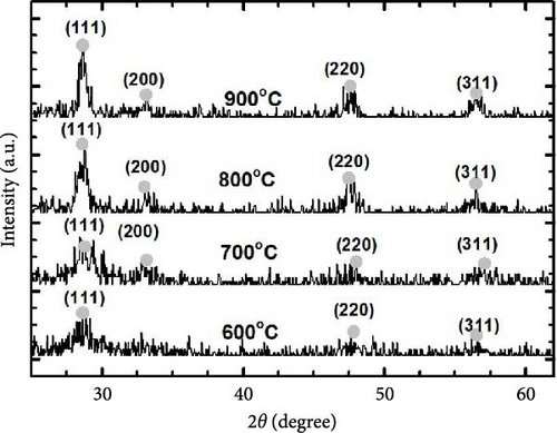
Figure 1 presents GIXRD patterns of GaxCeyOz PL deposited on 4H-SiC substrates and annealed at 600–900°C in a controlled N2–O2–N2 ambient. All GaxCeyOz PL exhibited a polycrystalline phase, with peaks corresponding to the (111), (200), (220), and (311) planes of the cubic fluorite CeO2 structure (ICDD 00-034-0394). Notably, the (200) plane was absent in the 600°C annealed sample. Phase separation was ruled out, as no peaks corresponding to monoclinic (ICDD 00-041-1103) or cubic Ga2O3 (ICDD 00-020-0426) were observed. The absence of phase separation in the GIXRD analysis confirms the successful incorporation of Ga3+ into the CeO2 lattice, forming a homogeneous solid solution. In the case of phase separation, random grain orientation leads to non-uniformity in the electrical characterization of the PL, which is undesirable [41]. Therefore, no phase separation in the present study is a significant advantage, as it ensures uniform dielectric properties, minimizes defect sites, and enhances interfacial quality with the 4H-SiC substrate. The single-phase structure contributes to improved electrical performance, including a higher effective dielectric constant, reduced leakage current, and better breakdown voltage, which are critical for high k PL applications. This homogeneity also underscores the thermodynamic stability of Ga3+ doped CeO2 under the optimized processing conditions, further validating the robustness of the present approach. Further investigation has disclosed that all of the diffraction peaks were moved to a higher diffraction angle in comparison to the ICDD file no. 00-034-0394 denoting the incorporation of the trivalent Ga3+ cation with a smaller ionic radius (0.62 Å) than Ce4+ (0.97 Å) into the CeO2 crystal lattice has been successful, aiding the formation of ternary GaxCeyOz phase.
Details are in the caption following the image
GIXRD patterns of gallium cerium oxide (GaxCeyOz) passivation layer (PL) annealed in N2–O2–N2 ambient at 600, 700, 800 [40], and 900°C.
The modification of the CeO2 crystal lattice with the introduction of Ga3+ cation would trigger an alteration in the crystal lattice parameters (a). The a values were determined using the following equation [42]:
(1)
(2)
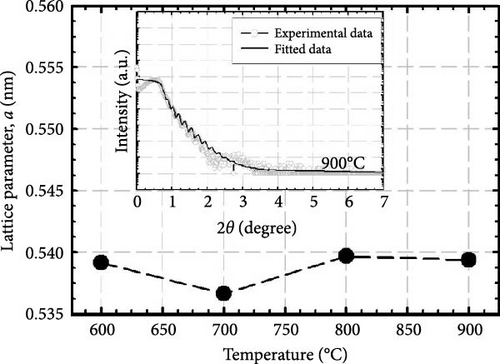
where dhkl, θ, and (hkl) are the interplanar spacing, diffraction angle, and Miller’s index, respectively. Figure 2 depicts the computed a values wherein it was noticed that all of the studied GaxCeyOz PL exhibited crystal lattice contraction in comparison to standard CeO2 (a = 0.5411 nm). This supported the notion that Ga3+ ions, which have a smaller ionic radius than Ce4+ ions, were successfully incorporated into the CeO2 crystal lattice, forming the GaxCeyOz phase. Besides, a sudden reduction in the a value was observed as the annealing temperature was increased from 600 to 700°C. This observation suggested the generation of a higher concentration of Vo at this temperature, leading to the smallest a value among the investigated PL. As the annealing temperature underwent a transition to reach the elevated value of 700°C, it was anticipated that this alteration in thermal conditions would consequently facilitate the movement and migration of a significantly greater quantity of nitrogen ions within the GaxCeyOz PL. It is possible that these nitrogen ions have a higher likelihood of diffusing toward the region of GaxCeyOz PL compared to the interface [16]. Hence, the nitrogen ions located at the region of GaxCeyOz PL have formed an attachment with the Vo in the GaxCeyOz crystal lattice, wherein charge neutrality of the GaxCeyOz crystal lattice was achieved through the release of adjacent oxygen ions. As a result, newly formed Vo were being introduced into the GaxCeyOz crystal lattice subjected to annealing at 700°C, aiding the attainment of a smaller a value in comparison to GaxCeyOz PL annealed at 600°C. The above statement could be further supported by the obtained EDX results (Table 1), which has revealed that the atomic percentage (at%) of nitrogen was changed from 6.04 to 9.30 at% at 700°C.
Details are in the caption following the image
Lattice parameters of gallium cerium oxide (GaxCeyOz) passivation layer (PL). The inset of this figure shows the experimental and computationally fitted X-ray reflectivity (XRR) result for GaxCeyOz PL annealed at 900°C.
Table 1. The constituent elements extracted from the EDX measurements for the GaxCeyOz PL.
Annealing temperatures (°C) O (at. %) Ce (at. %) Ga (at. %) N (at. %)
600 60.57 20.43 12.96 6.04
700 59.39 21.02 10.28 9.30
800 61.72 20.15 8.78 9.35
900 65.59 18.02 8.70 7.69

Upon elevating the postdeposition annealing temperature to 800°C, a marginal increase in the nitrogen content was recorded, reaching a level of 9.35 at%, which indicates a heightened diffusion phenomenon of nitrogen ions into the GaxCeyOz PL. The application of a significantly elevated annealing temperature of 800°C has provided an augmented amount of thermal energy, thereby facilitating a more pronounced influx of nitrogen ions that are capable of migrating toward the critical interface region that exists between the GaxCeyOz PL and the underlying 4H-SiC substrate. Consequently, this scenario has led to a diminished probability of nitrogen ions persisting within the GaxCeyOz crystalline lattice structure when compared to the interface. Therefore, the nitrogen ions that have gathered in proximity to the interface region have established bonds with the dangling bonds of silicon and/or carbon [43], which in turn has effectively hindered the reactive interactions between oxygen ions and the surface of 4H-SiC, thereby serving to reduce the formation of SiO2 IL. Therefore, the oxygen ions have diffused outward, consequently increasing the probability of oxygen ions being attached to the Vo site in the GaxCeyOz crystal lattice while undergoing annealing at 800°C, resulting in lattice expansion. However, a reduction in a was attained at a maximum annealing temperature of 900°C. The abrupt decrease in a value observed at 900°C may be attributed to the oxygen ions acquiring adequate energy to disrupt the bonding of nitrogen ions with the Si and/or C dangling bonds [16], wherein these nitrogen ions have diffused outward from the GaxCeyOz PL contributing to the reduction in at% of nitrogen (7.69 at%). The disruption of the attachment between nitrogen ions and the dangling bonds of Si and/or C while annealing to 900°C could also be reinforced by reaching the maximum at% of oxygen, allowing oxygen ions with adequate energy to diffuse into the GaxCeyOz PL to disrupt these attachments.

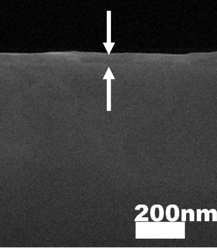
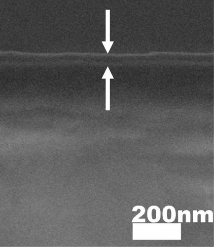
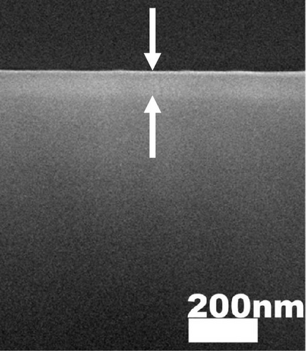
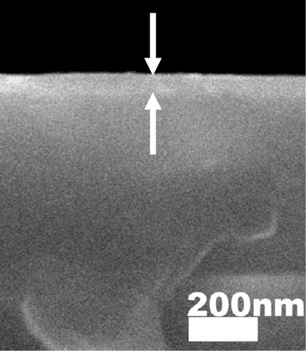
The cross-sectional FESEM images of the investigated GaxCeyOz PLs were presented in Figure 3, as the information related to the average total oxide thickness of the investigated PLs was extracted from 10 different locations using ImageJ software (Table 2). It was noticed that the GaxCeyOz PLs were undergoing a densification process when postdeposition annealing was carried out from 600 to 800°C as the measured average total oxide thickness ranging from 71.0 to 45.7 nm was lower than the average total oxide thickness of the as-deposited GaxCeyOz PL (186.2 nm) [40]. This observation has suggested that during postdeposition annealing from 600 to 800°C, oxygen ions could be filling the Vo in the GaxCeyOz crystal lattice as well as the removal of defects that would aid in the densification of the GaxCeyOz PL [44]. At 700°C, the GaxCeyOz PL exhibited a higher concentration of newly formed oxygen vacancies (Vo), resulting in less pronounced densification compared to the GaxCeyOz PL at 800°C. However, at 900°C, the average total oxide thickness showed a slight increase to 47.4 nm, compared to 45.7 nm for the GaxCeyOz PL annealed at 800°C. The increase in oxide thickness during postdeposition annealing at 900°C indicates that the formation of a SiO2 IL was more significant at this temperature, while it is suggested that SiO2 IL formation may be less prominent at or below 800°C.
Details are in the caption following the image
Cross-sectional field-emission scanning electron microscopy (FESEM) images of gallium cerium oxide (GaxCeyOz) passivation layer (PL) annealed in N2–O2–N2 ambient at (a) 600, (b) 700, (c) 800 [40], and (d) 900°C.
Details are in the caption following the image
Cross-sectional field-emission scanning electron microscopy (FESEM) images of gallium cerium oxide (GaxCeyOz) passivation layer (PL) annealed in N2–O2–N2 ambient at (a) 600, (b) 700, (c) 800 [40], and (d) 900°C.
Details are in the caption following the image
Cross-sectional field-emission scanning electron microscopy (FESEM) images of gallium cerium oxide (GaxCeyOz) passivation layer (PL) annealed in N2–O2–N2 ambient at (a) 600, (b) 700, (c) 800 [40], and (d) 900°C.
Details are in the caption following the image
Cross-sectional field-emission scanning electron microscopy (FESEM) images of gallium cerium oxide (GaxCeyOz) passivation layer (PL) annealed in N2–O2–N2 ambient at (a) 600, (b) 700, (c) 800 [40], and (d) 900°C.
Table 2. The estimated thicknesses of GaxCeyOz PL and SiO2 IL from XRR measurements as total oxide thickness of GaxCeyOz PL extracted from XRR as well as cross-sectional FESEM measurements.
Annealing temperature (°C) XRR: GaxCeyOz thickness (nm) XRR: SiO2 thickness (nm) XRR: total oxide thickness (nm) Cross-sectional FESEM: total oxide thickness (nm)
600 74.128 1.466 75.594 71.0
700 56.143 2.976 59.119 58.4
800 44.378 [40] 3.258 [40] 47.636 [40] 45.7 [40]
900 43.921 4.723 48.644 47.4

XRR measurements were employed to assist in evaluating trends in film density and the presence of a SiO2 IL in GaxCeyOz PL at various postdeposition annealing temperatures. The experimental and fitted XRR curve for the GaxCeyOz PL annealed at 900°C is shown in the inset of Figure 2. Table 2 summarizes the thickness of the GaxCeyOz PL and SiO2 IL across different annealing temperatures. The XRR results provided a clearer view, revealing that as the postdeposition annealing temperature increased from 600°C to 900°C, the GaxCeyOz PL thickness reduced from 74.128 to 43.921 nm, indicating densification. Additionally, the thickness of the SiO2 IL increased from 1.466 to 4.723 nm with increasing annealing temperature, suggesting that higher oxygen ion diffusivity to the interface was temperature-dependent. Table 2 shows a significant variation in SiO2 IL thickness (1.510 nm) as the temperature switched to 700°C from 600°C, consistent with earlier explanations that nitrogen ions accumulate in the GaxCeyOz PL region, forming bonds with Vo [16]. This leads to oxygen ions released during nitrogen attachment with Vo, along with inward-diffusing oxygen ions during the dwelling stage, diffusing to the interface and reacting with the 4H-SiC surface, promoting SiO2 IL formation. In contrast, SiO2 IL formation slowed down at 800°C, likely due to nitrogen ion migration to the interface. The nitrogen ions at the interface act as a barrier, preventing oxygen ions from reacting with the 4H-SiC surface, resulting in a smaller SiO2 IL thickness variation (0.282 nm) when the temperature increased from 700 to 800°C. The nitrogen ions’ effectiveness in limiting SiO2 IL formation diminished at 900°C, where a larger variation in SiO2 IL thickness (1.465 nm) was observed between the samples annealed at 800 and 900°C. This increase in SiO2 IL thickness suggested that oxygen ions had enough energy to break nitrogen bonds with the Si and/or C dangling bonds, allowing oxygen ions to react with the 4H-SiC surface. While SiO2 IL formation intensified at 900°C, the use of the GaxCeyOz PL on the 4H-SiC substrate effectively controlled SiO2 IL thickness (4.723 nm) compared to GaxCeyOz (24.239 nm) [29] and CeO2 (40.194 nm) [17] PLs deposited on Si substrates subjected to similar annealing conditions.
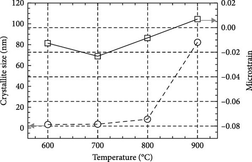
In an effort to determine and accurately extract the crystallite size (D), as well as the microstrain (ε), of the GaxCeyOz PL that were subjected to various annealing temperatures in N2–O2–N2 ambient, the well-established Williamson–Hall (W–H) method was employed, which can be succinctly articulated through the equation that follows [45]:
(3)
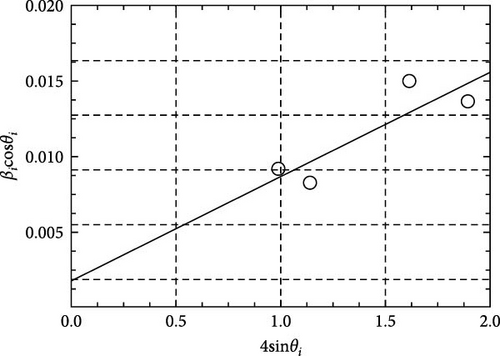
where λ, θi, βi are X-rays source wavelength (λ = 1.5406 Å), diffraction angle of the (hkl) diffraction peak, and integral breadth (in radius 2θ) of the ith Bragg reflection positioned at 2θi. The typical W–H plot for the GaxCeyOz PL annealed at 900°C subjected to linear fitting (Figure 4) to ascertain the slope and intercept necessary for the determination of ε and D, respectively, with the resultant values illustrated in Figure 5. As a whole, it was noticed that the values of D were enhanced with respect to annealing temperatures, indicating that the smaller crystallites were undergoing a coalescence process to form larger crystallites. Among all the examined samples, it was observed that the minimal increase in D was achieved when the annealing temperature was elevated from 600 to 700°C. The rationale behind this observation may be attributed to the migration of a significant concentration of nitrogen ions toward the GaxCeyOz PL region at 700°C, where the presence of excess nitrogen ions has impeded the coalescence of crystallites. Additionally, the attachment of nitrogen ions to the Vo in GaxCeyOz crystal lattice contributing to the release of oxygen ions as well as the attachment of trivalent Ga3+ cation with the Vo to form Ga3+Vo defect pairs [34] have slowed down the coalescence process of forming larger crystallites. Hence, it was noticed that the largest compressive ε was induced on the GaxCeyOz PL annealed at 700°C due to the highest concentration of nitrogen ions accumulated at the region of PL, attachment of nitrogen ions to Vo, formation of new Vo, as well as formation of Ga3+Vo defect pairs. As the annealing temperature increased to 800°C, a reduction in compressive strain (ε) in the GaxCeyOz passivation layer (PL) promoted the growth of larger domains (D). This effect might be attributed to the accumulation of a higher concentration of nitrogen ions at the interface, which likely hindered the diffusion or reaction of oxygen ions with the 4H-SiC surface. Hence, these unreacted oxygen ions might have diffused outward and occupied the Vo in the GaxCeyOz crystal lattice to assist in the coalescence process of forming larger crystallites. Nonetheless, a substantial increment in D was discerned at the maximum temperature of 900°C was being utilized. Therefore, it was presumed that a higher concentration of oxygen ions has diffused into this GaxCeyOz PL with higher energy at 900°C, of which the oxygen ions may knock off the nitrogen ions attached to Vo in GaxCeyOz crystal lattice as well as breaking the attachment of nitrogen ions with the Si and/or C dangling bonds. Consequently, the inward diffusing oxygen ions could occupy the Vo being formed from the knockoff of nitrogen ions attached to Vo in GaxCeyOz that would assist in the formation of the largest D as well as the generation of tensile ε being induced on the GaxCeyOz PL annealed at 900°C. A comparable trend of increasing microstrain with increasing crystallite size has been previously reported in studies involving Ce-doped CuO thin films [46].
Details are in the caption following the image
Typical Williamson-Hall (W–H) plot for gallium cerium oxide (GaxCeyOz) passivation layer (PL) at 900°C.
Details are in the caption following the image
Crystallite size and microstrain for gallium cerium oxide (GaxCeyOz) passivation layer (PL).

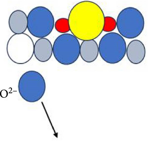
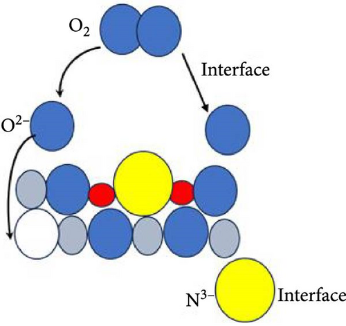
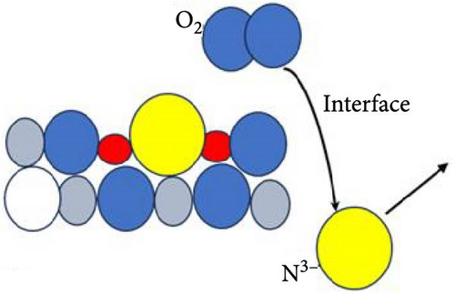
Figure 6 delineates the overarching mechanism that transpires within the GaxCeyOz/4H-SiC system. Initially, Ga3+ cations are posited to occupy the Ce4+ sites within the CeO2 lattice, thereby facilitating the formation of GaxCeyOz PL material while concomitantly generating Vo to achieve charge neutrality (Figure 6a). During the annealing process, with the infusion of nitrogen ions (N3−), a portion of these nitrogen ions is hypothesized to interact with the vacancies, while others may migrate to the interface to form bonds with silicon and/or carbon dangling bonds (Figure 6b). At the comparatively lower temperature of 600°C, it was noted that the N3− ions predominantly occupied the available Vo sites within the GaxCeyOz PL. As the temperature was elevated to 700°C, the propensity for N3− ions to diffuse toward the interface increased. Simultaneously, the binding of N3− ions to the Vo resulted in the liberation of additional O2− ions, thereby generating more Vo to maintain charge equilibrium (Figure 6c). The liberated oxygen ions may either migrate to the interface to form a SiO2 IL or diffuse out of the PL. The application of a higher thermal treatment at 800°C has imparted a heightened amount of thermal energy, consequently promoting a more significant influx of nitrogen ions capable of traversing toward the critical interface region that exists between the GaxCeyOz PL and the underlying 4H-SiC substrate. This phenomenon has consequently resulted in a reduced likelihood of nitrogen ions remaining within the GaxCeyOz crystalline lattice structure in contrast to their presence at the interface. Hence, the nitrogen ions that have concentrated near the interface region have formed bonds with the dangling bonds of silicon and/or carbon, thereby effectively obstructing the reactive interactions between oxygen ions and the surface of 4H-SiC, which in turn has mitigated the formation of the SiO2 IL. Consequently, the oxygen ions have diffused outward, thereby augmenting the likelihood of oxygen ions attaching to Vo sites (Figure 6d) in the GaxCeyOz crystal lattice during the annealing process at 800°C. However, at 900°C, the oxygen ions acquired sufficient energy to disrupt the bonding interactions between nitrogen ions and the silicon and/or carbon dangling bonds (Figure 6e), resulting in the outward diffusion of these nitrogen ions from the GaxCeyOz PL. Furthermore, these oxygen ions have also accelerated the passivation of vacancies, facilitating the reoxidation of Ce3+ to Ce4+ at the temperature of 900°C.
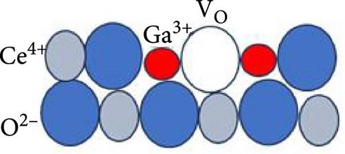
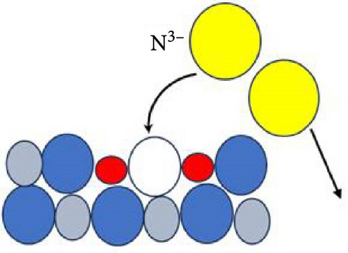
Details are in the caption following the image
Schematic diagram for the mechanism involved within the gallium cerium oxide (GaxCeyOz)/4H-silicon carbide (4H-SiC) system, consisting of (a) formation of GaxCeyOz PL, (b) interaction of N3− with oxygen vacancies, (c) liberation of O2− ions from lattice, (d) attachment of O2− with oxygen vacancies, and (e) outward diffusion of N3− ions.
A further analysis on the formation of GaxCeyOz PLs on 4H-SiC substrate has been carried out by extracting the direct (ED) and indirect (EID) bandgaps of these samples based on attained UV–VIS spectra. The acquired UV–VIS results were modeled using the Kubelka–Munk (KM) function, as expressed below [47]:
(4)
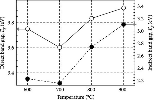
where R is regarded as the diffuse reflectance, with the F (R) function being scaled by hv, employing 1/2 and 2 as the respective coefficients (n) for direct-band and indirect-band optical transitions. The ED and EID values were computed as per (F (R) x hv)2 vs. hv and (F (R) x hv)1/2 vs. hv plots, respectively, via extrapolation of the linear region to zero (not shown) and are presented in Figure 7. The deduction from Figure 7 that the extracted ED and EID values within the range of 3.83–3.91 eV as well as 2.74–3.10 eV, respectively, for the GaxCeyOz PLs annealed at 800 and 900°C were lies in the range of the reported ED (4.85 eV) and EID (4.66 eV) for Ga2O3 as well as ED (3.12 eV) and EID (2.58 eV) for CeO2 [29]. These results have further complimented the other reported results in this work that the modification of CeO2 crystal lattice with Ga3+ cations has been attained by the formation of GaxCeyOz PLs [16]. Nonetheless, it was noticed that a smaller ED (3.60–3.75 eV) and EID (2.15–2.22 eV) values were obtained by the PLs annealed at 600 and 700°C, which could be related to either the attachment of a higher concentration of nitrogen ions to the Vo or/and the existence of a higher concentration of the Vo in GaxCeyOz crystal lattice. A similar observation of bandgap narrowing due to oxygen vacancy-induced gap states was observed for the HfO2 PL on the 4H-SiC semiconductor [48]. Additionally, it should be noted that the doping of a higher at% nitrogen ion for the GaxCeyOz PL annealed at 700°C has introduced N 2p states that have contributed to the narrowing of bandgap through the raising of valance band maximum [49]. Although the EDX analysis disclosed the acquisition of a slightly higher at% of nitrogen ions by the GaxCeyOz PL annealed at 800°C than that of 700°C, the acquisition of larger ED and EID values for the sample annealed at 800°C has further supported the fact that a higher concentration of nitrogen ions were being diffused to the region of interface between GaxCeyOz PL and 4H-SiC substrate. Hence, the influence of nitrogen ions attaching to the Vo of the GaxCeyOz crystal lattice toward the narrowing of ED and EID was less significant when the GaxCeyOz PLs were subjected to annealing at 800°C when compared with 700°C.
Details are in the caption following the image
Direct and indirect bandgap for gallium cerium oxide (GaxCeyOz) passivation layer (PL) annealed in N2–O2–N2 ambient at 600, 700, 800 [40], and 900°C.

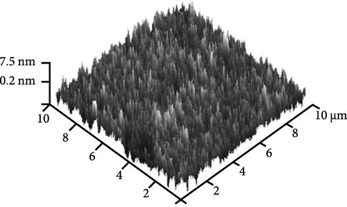
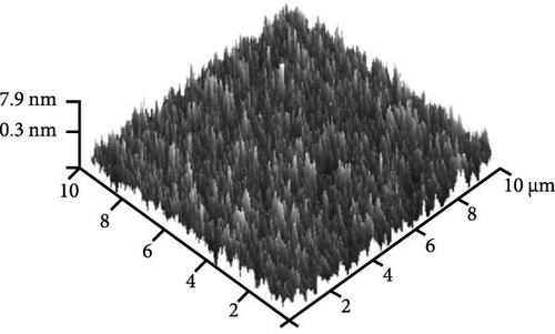
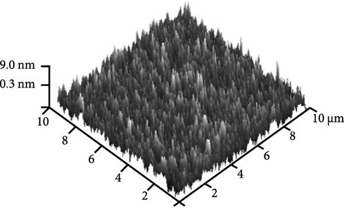
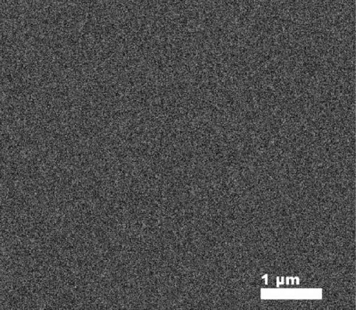
Figure 8e shows the typical FESEM surface morphology of the investigated GaxCeyOz PL that was annealed at 900°C. It was noticed that the surface of all GaxCeyOz PLs was smooth without observable cracks or voids. AFM characterization was employed to obtain the 3-dimensional surface topographies of the investigated PLs, as presented in Figure 8. The 3-dimensional surface topography (Figure 8a) for the GaxCeyOz PL annealed at 600°C has disclosed the formation of smaller dimension protrusions with random distribution throughout the surface of GaxCeyOz PL. As the annealing temperature was increased to 700 (Figure 8b) and 800°C (Figure 8c), the distribution of protrusions was more uniform with a vertical growth of protrusions on the surface of this GaxCeyOz PL. With the employment of a maximum temperature of 900°C, the migration of more oxygen ions toward the region of GaxCeyOz PL has further stimulated the growth of protrusions, wherein the formation of the larger dimension of protrusions was observed in Figure 8d. As a whole, the RMS roughness values were enhanced from 0.94 to 2.53 nm with respect to annealing temperatures (Figure 8).
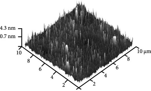
Details are in the caption following the image
Three-dimensional surface topographies for gallium cerium oxide (GaxCeyOz) passivation layer (PL) subjected to postdeposition annealing in N2–O2–N2 ambient at (a) 600, (b) 700, (c) 800 [40], and (d) 900°C. (e) Depicts the typical field-emission scanning electron microscopy (FESEM) surface morphology of GaxCeyOz PL annealed at 900°C.

Figure 9 presents the leakage current density-electric field (J–E) characteristics of the GaxCeyOz PLs annealed at different temperatures in N2–O2–N2 ambient. As a whole, it was noticed that the GaxCeyOz PLs annealed at 800 and 900°C have demonstrated higher electric breakdown field (EB) of 2.95 and 5.58 MV/cm, respectively, when compared with the GaxCeyOz PLs annealed at 600 (0.51 MV/cm) and 700°C (1.06 MV/cm). A substantial improvement in the EB for GaxCeyOz PLs annealed at 800 and 900°C could be related to the existence of a lower density of defects with regards to Vo, wherein the attainment of larger ED and EID when compared with GaxCeyOz PLs annealed at 600 and 700°C has suggested that a higher concentration of oxygen ions have occupied the Vo within the GaxCeyOz lattice, aiding the reduction of the density of defects. Moreover, the employment of annealing at 700°C has offered an adequate amount of energy for more nitrogen ions to diffuse to the region of GaxCeyOz PL in which these nitrogen ions would either attach to the Vo, contributing to the formation of new Vo to achieve charge neutrality or the unbonded nitrogen ions lingering at the region of GaxCeyOz PL. As a consequence, the GaxCeyOz PL subjected to annealing at 700°C has demonstrated a poorer J–E characteristic than GaxCeyOz PL annealed at/beyond 800°C due to the narrowing of ED and EID as a result of nitrogen ions attached to the Vo in GaxCeyOz crystal lattice as well as the presence of negatively charged defects, namely, unbonded nitrogen ions in the region of GaxCeyOz PL that would act as scattering center for the injected electrons to break the bonding of GaxCeyOz when E was being applied. Of these investigated samples, the GaxCeyOz PL annealed at 600°C has demonstrated the poorest J–E characteristic due to the acquisition of the lower at% nitrogen as disclosed by EDX (Table 1), wherein the probability of incorporated nitrogen attaching to Vo and migrating toward the interface to passivate Si and/or C dangling bonds [16] was the lowest amongst the investigated GaxCeyOz PL.
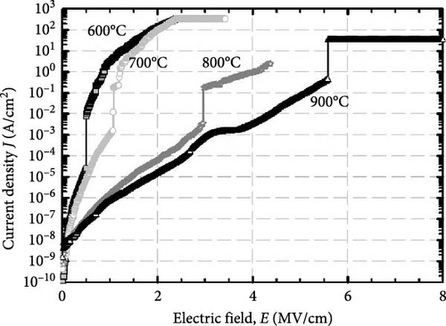
Details are in the caption following the image
Leakage current density-electric field (J–E) characteristics of gallium cerium oxide (GaxCeyOz) passivation layer (PL) subjected to postdeposition annealing in N2–O2–N2 ambient at 600, 700, 800 [40], and 900°C.
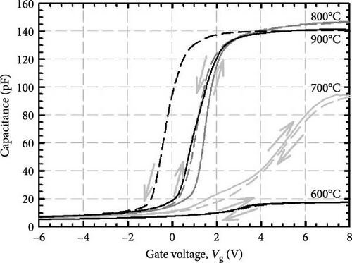
Although XRR measurements have revealed the formation of thicker low k SiO2 IL for the GaxCeyOz PLs annealed at 800 and 900°C, the detrimental effects caused by this low k SiO2 IL could be minimal as better J–E characteristics have been displayed by these two samples when compared with samples annealed at lower temperatures. The capacitance–voltage (C–V) measurements at the frequency of 1 MHz were carried out by sweeping the gate voltage from −6 to +8 V, as presented in Figure 10, to assess the influence of SiO2 IL formation toward the k values of the investigated GaxCeyOz PL. Based on the attained C–V curves, the k values were calculated using the following equation [50]:
(5)
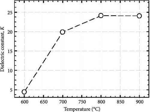
where Cox, tox, εo, and A indicate the accumulation level capacitance, total oxide thickness, permittivity of free space, and area of metal contact, respectively. The estimated k values at varying annealing temperatures are depicted in Figure 11. It was determined that the GaxCeyOz PL annealed at 600°C obtained an appreciably low k value of 4.43, which was in agreement with the earlier explanation that the highest density of defects was formed in this PL contributing to the attainment of the lowest EB and the highest J. When the GaxCeyOz PL were subjected to annealing temperature at/beyond 700°C, a substantial increment in k values was noticed even though XRR measurements have revealed the formation of thicker SiO2 IL with respect to annealing temperature. It is plausible to infer that the development of low k SiO2 IL may have a minimal impact on the overall k value of the GaxCeyOz PL that were subjected to annealing processes within the temperature range of 700–900°C in N2–O2–N2 ambient. The underlying rationale that leads to the observation of a comparatively lower k value of 19.85 for the GaxCeyOz at 700°C, especially when juxtaposed with the outcomes observed at elevated annealing temperatures, can be attributed to the accumulation of nitrogen ions within the region of the GaxCeyOz PL; this accumulation facilitates the interaction and bonding of nitrogen ions with Vo, ultimately resulting in the creation of additional Vo states. Since more nitrogen ions were diffused to the interface between GaxCeyOz PL and 4H-SiC substrate at 800°C, the inward diffusing oxygen ions would be able to occupy the Vo in GaxCeyOz to reduce the density of defects in this PL leading to the attainment of a higher k value of 24.11. A slight reduction in the k value, quantified at 0.1, was recorded when the annealing temperature was elevated from 800 to 900°C; this finding is particularly intriguing given that the XRR measurements have indicated the presence of a more pronounced variability in the thickness of the SiO2 IL, which measured ~1.464 nm for the two distinct samples in question. This particular observation strongly suggested that the development of a thicker SiO2 IL at the elevated annealing temperature of 900°C exerts a negligible influence on the k value as well as the J–E characteristics of this specific PL.
Details are in the caption following the image
Capacitance-voltage (C–V) curves for gallium cerium oxide (GaxCeyOz) passivation layer (PL) annealed in N2–O2–N2 ambient at 600, 700, 800 [40], and 900°C.
Details are in the caption following the image
Dielectric constant values for gallium cerium oxide (GaxCeyOz) passivation layer (PL) at 600, 700, 800 [40], and 900°C.

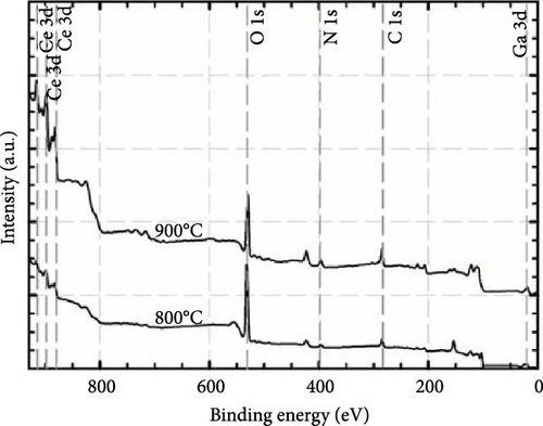
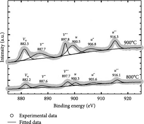
It is worth mentioning the GaxCeyOz PLs annealed at 800 and 900°C have demonstrated superior J–E characteristics as well as k values, and of which further investigation on the chemical composition present in these PLs was conducted using XPS characterization. Figure 12 presents the survey spectrum obtained for the GaxCeyOz PLs annealed at 800 and 900°C. Based on this, the XPS peaks corresponding to Ce 3d, O 1s, Ga 3d, and N 1s were identified and are shown in Figure 13. The XPS peaks were calibrated based on the C 1s peak located at 284.6 eV for the GaxCeyOz PL annealed at 800 and 900°C. Deconvolution of a well-resolved spectrum of the Ce 3d core level at an energy range of 870–930 eV resulted in the identification of six distinct peaks, as depicted in Figure 13a. It was noted that the GaxCeyOz PL, subjected to annealing temperatures of 800 and 900°C, yielded Ce4+−related peaks at energies of 887.6 (v″), 897.7 (v‴), 900.3 (u), 905.6 (u″), and 916.1 eV (u‴), as well as 887.7, 897.8, 900.5, 906.8, and 916.3 eV, respectively. The Ce4+ states have been discerned by examining the emission originating from the Ce 3d5/2 (v″ and v‴) as well as the emission originating from the Ce 3d3/2 core levels (u, u″, and u‴) [51]. Moreover, the Ce3+-related peak was detected at 882.2 (Vo) and 882.3 (Vo) originating from s annealed at 800 and 900°C, respectively. Although the detection of Ce3+ states suggested the formation of Vo was accompanied by the reduction of Ce4+ to Ce3+, the detection of only one peak for the investigated samples suggested that the concentration of Vo was minimal at these temperatures. Moreover, shifting toward the lower binding energy for all of the peaks as compared to the reported peak position related to the Ce 3d core spectra suggested the successful doping of a trivalent Ga3+ cation into the CeO2 crystal lattice to form the GaxCeyOz PL [52, 53]. In addition, shifting in the position of identified peaks toward higher binding energy was witnessed as the annealing temperature was increased from 800 to 900°C. This observation suggested the reoxidation of the Ce3+ to the Ce4+ state has taken place at 900°C by releasing electrons from the Ce state [54]. The aforementioned observation aligned with the preceding explanation that a higher concentration of oxygen ions was incorporated into the GaxCeyOz PL at 900°C. In this context, the incorporated oxygen ions could not only diffuse to the interface but also passivate Vo, consequently leading to the possibility of reoxidation from the Ce3+ to Ce4+ state.
Details are in the caption following the image
X-ray photoelectron spectroscopy (XPS) survey-scan for gallium cerium oxide (GaxCeyOz) passivation layer (PL) annealed at 800 and 900°C.
Details are in the caption following the image
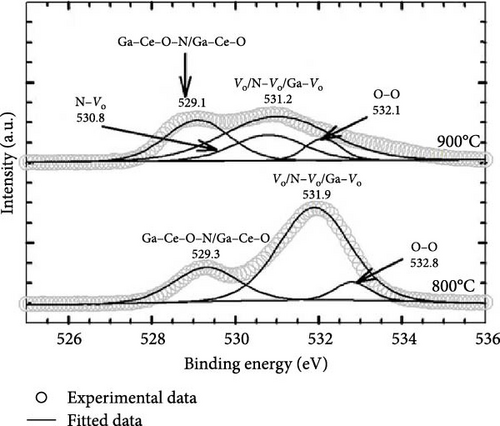
X-ray photoelectron spectroscopy (XPS) core level spectra of (a) Ce 3d, (b) O 1s, (c) Ga 3d, and (d) N 1s for gallium cerium oxide (GaxCeyOz) passivation layer (PL) annealed at 800 and 900°C.
Details are in the caption following the image
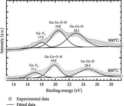
X-ray photoelectron spectroscopy (XPS) core level spectra of (a) Ce 3d, (b) O 1s, (c) Ga 3d, and (d) N 1s for gallium cerium oxide (GaxCeyOz) passivation layer (PL) annealed at 800 and 900°C.
Details are in the caption following the image
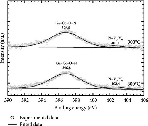
X-ray photoelectron spectroscopy (XPS) core level spectra of (a) Ce 3d, (b) O 1s, (c) Ga 3d, and (d) N 1s for gallium cerium oxide (GaxCeyOz) passivation layer (PL) annealed at 800 and 900°C.
Details are in the caption following the image
X-ray photoelectron spectroscopy (XPS) core level spectra of (a) Ce 3d, (b) O 1s, (c) Ga 3d, and (d) N 1s for gallium cerium oxide (GaxCeyOz) passivation layer (PL) annealed at 800 and 900°C.

Further clarity was obtained by deconvoluting O 1s spectra for the GaxCeyOz PL annealed at 800 and 900°C, and the resulting spectra are shown in Figure 13b. It is well known that the O 1s spectra peak is related to low energy (OL), mid energy (OM), and high energy (OH) ascribed to crystal lattice oxygen, Vo, and adsorbed oxygen, respectively [55]. Consequently, the OL peaks of 529.3 and 529.1 for the GaxCeyOz PL at 800 and 900°C, respectively, were ascribed to Ga–Ce–O–N bonding [56]. Moreover, the OM peak for the GaxCeyOz PL at 800 (531.9 eV) and 900°C (530.8 and 531.2 eV) was related to the Vo induced by the formation of Ga–Ce–O bonding or N–Vo or Ga–Vo defect cluster. The presence of an additional OM peak for the GaxCeyOz PL at 900°C suggested that the incoming oxygen ions have gained sufficient energy to break the nitrogen attachment with the Si and/or C dangling bonds, wherein some of the released nitrogen ions could have diffused inwards toward the region of the GaxCeyOz PL to form an attachment with the Vo. The shifting in binding energies to lower values that were observed with the increase in annealing temperature from 800 to 900°C provides additional verification for the preceding assertion that the conversion of Ce3+ to Ce4+ through reoxidation has been accomplished at 900°C. Consequently, the liberated electron from the Ce state would be captured by the O state, resulting in a decrease in binding energy. In addition, the OH peaks at 532.8 and 532.1 eV for the GaxCeyOz PL annealed at 800 and 900°C, respectively, were related to the additional oxygen ions in the interstitial positions [57].

Additional information on the formation of the GaxCeyOz phase was attained through the acquisition of Ga 3d (Figure 13c) spectra, wherein sharp peaks related to Ga–Ce–O–N bonding were observed for the GaxCeyOz PL annealed at 800°C (19.9 eV) and 900°C (19.8 eV). The peaks at 19.9 (800°C) and 19.8 eV (900°C) could be arising from the Ga 3d5/2 core level, while the peaks at 24.4 and 23.1 eV were due to Ga 3d3/2 core level emission suggesting the presence of Ga3+ states in the PL [58]. The peaks at 19.9 and 19.8 eV binding energies for the GaxCeyOz PL at 800 and 900°C were ascribed to Ga–Ce–O–N bonding as it was within the range of reported Ga–N (19.6 eV) [59] and Ga–O (21.9 eV) [60] bonding positions. Moreover, the peaks of 24.4 and 23.1 eV for the GaxCeyOz PL at 800 and 900°C, respectively, were attributed to the formation of Ga–Ce–O bonding, wherein the lower binding energy observed for the sample at 900°C further supported that reoxidation of Ce3+ to Ce4+ occurred at 900°C, improving the passivating characteristics of the GaxCeyOz PL (Table 1). In addition, it should be noted that, as no phase separation was detected by the GIXRD (Figure 1), the XPS analysis further supported the idea that Ga3+ could be mainly residing at GaCe sites at the CeO2 crystal lattice, leading to the formation of the GaxCeyOz phase. The presence of a low-intensity peak at 17.1 and 17.9 eV in the GaxCeyOz PL provided evidence for the existence of the Ga–Vo defect cluster [61]. The N 1 s spectra were deconvoluted, revealing the emergence of two distinct peaks, as illustrated in Figure 13d, where one prominent peak was observed at energy levels of 396.8 eV and 396.5 eV for the GaxCeyOz PL annealed at a temperature of 800 and 900°C, respectively, thereby providing further corroborative evidence for the incorporation of nitrogen within the crystalline lattice structure of CeO2. It has been previously documented in the literature that the specific bonding positions associated with the N 1s spectra for N–O, Ce–N, and Ga–N, which have been identified at binding energies of 393.7 [62], 396.1 [63], and 397.3 eV [63], respectively, according to prior studies. Hence, 396.8 and 396.5 can be ascribed to the Ga–Ce–O–N bonding. Moreover, the relatively low-intensity peak observed at 402.4 and 401.1 at 800 and 900°C, respectively, could be due to the attachment of nitrogen to the oxygen vacancy site, leading to the formation of N–Vo bonding or Vo states resulted from the breaking of the attachment [64].
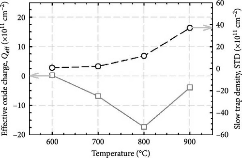
By referring to the C–V curves presented in Figure 10, a positive flat band voltage shift (∆VFB) was observed for all samples, suggesting the presence of negatively charged traps in the investigated GaxCeyOz PL. The quantity of negatively charged traps present in the investigated GaxCeyOz PL could be estimated by determining the effective oxide charge (Qeff) using the following equation [65]:
(6)
where q represents the charge of electron. The computed Qeff in the present work is shown in Figure 14. The acquisition of the lowest magnitude of negative Qeff value for the GaxCeyOz PL annealed at 600°C has further reinforced that a lower concentration of negatively charged nitrogen ions have diffused into the region of GaxCeyOz PLs, wherein EDX characterization has revealed attainment of the lowest at% of nitrogen. When the annealing temperature was enhanced to 700°C, the migration of a higher concentration of negatively charged nitrogen ions to the region of GaxCeyOz PL have contributed to the attainment of a higher magnitude of negative Qeff value than that of the GaxCeyOz PL annealed at 600°C. Although the EDX measurements have revealed that a minute variation in the at% of nitrogen for both GaxCeyOz PLs annealed at 700 (9.30 at%) and 800°C (9.35 at%) was obtained, a substantial increment in the magnitude of negative Qeff value from −6.82 × 1011 to −17.29 × 1011 cm−2 has further reinforced the earlier explanation that the increment of annealing temperature to 800°C has stimulated the migration of more nitrogen ions to the region of interface between GaxCeyOz PL and 4H-SiC substrate. Another plausible explanation that may elucidate the phenomenon leading to the observation of the most pronounced Qeff value for the GaxCeyOz PL that has undergone annealing at a temperature of 800°C could very well be associated with the accumulation of nitrogen ions at the interface, which, in turn, functions as an effective barrier layer that serves to significantly mitigate the potential for oxygen ions to engage in reactive interactions with the surface of the 4H-SiC substrate. Hence, these unreacted oxygen ions would diffuse outward to occupy the positively charged Vo in the GaxCeyOz crystal lattice leading to the existence of more negatively charged traps in the. Nonetheless, a sudden reduction in the magnitude of negative Qeff value was perceived when the highest annealing temperature of 900°C was being utilized. The reason contributing to the reduction of negative Qeff value could be related to the oxygen ions gaining sufficient energy to knock off the nitrogen ions attached to the Vo in the GaxCeyOz crystal lattice, followed by these oxygen ions occupying these Vo. In addition to the aforementioned observations, it is noteworthy that the migration of oxygen ions toward the interface at a temperature of 900°C was not only capable of disrupting the nitrogen barrier layer but also facilitated the diffusion of negatively charged nitrogen ions away from the GaxCeyOz photoluminescent layer, as evidenced by the significant reduction in the at% of nitrogen, which decreased to 7.69 at%, thereby contributing to the realization of a notably lower magnitude of the Qeff, when compared to the GaxCeyOz PL that underwent annealing processes at the lower temperatures of 700 and 800°C.
Details are in the caption following the image
Effective oxide charge (Qeff) and slow trap density (STD) for gallium cerium oxide (GaxCeyOz) passivation layer (PL) at 600, 700, 800 [40], and 900°C.
It was evident from the C–V curves (Figure 10) that when measurements were being swept from negative voltage to positive voltage and vice versa, hysteresis was observed for all of the investigated GaxCeyOz PL, indicating the existence of slow trap density (STD), which could be estimated using the following equation [66]:
(7)
where ΔV is the difference between forward and reverse bias flatband voltage. The estimated STD values for the investigated GaxCeyOz PLs are depicted in Figure 14. It was noticed that the GaxCeyOz PLs annealed at 600 and 700°C have attained lower STD, although the C–V curves for both PLs have demonstrated a clockwise hysteresis denoting the presence of scattering center in these samples. Although scattering centers were present in these GaxCeyOz PLs annealed at 600 and 700°C, acquisition of the lowest STD has implied that the scattering center might be located near to the interface, wherein the injected electrons from 4H-SiC semiconductor during forward bias were being scattered further away from the interface. Hence, a lower density of electrons was being trapped during forward bias for the GaxCeyOz PLs annealed at 600 and 700°C resulting in the acquisition of a lower STD as a lower density of trapped electrons was available to be detrapped during reverse bias when compared with the GaxCeyOz PLs annealed at 800 and 900°C. Moreover, it was distinguished that anticlockwise hysteresis was acquired by the GaxCeyOz PLs annealed at 800 and 900°C signifying the presence of a lower density of scattering center in which more electrons were being trapped at the location nearer to the interface during forward bias. When reverse bias was being applied, the probability of these trapped electrons were being detrapped would be higher, and thus, a higher STD was attained by the GaxCeyOz PLs annealed at 800 and 900°C when compared with samples annealed at lower annealing temperatures. Another possible reason for the GaxCeyOz PL annealed at 900°C to attain a higher STD than 800°C due to the breaking of the nitrogen barrier layer near to the interface in which more traps are available at the interface to trap and detrap the electrons injected from the 4H-SiC substrate during forward and reverse bias, respectively.
A further evaluation on the formation of traps in determining interface quality was carried out employing Terman’s method, in which the equation mentioned below was used to calculate the interface trap density (Dit) for the GaxCeyOz PL [67]:
(8)
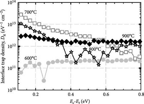
where ΔVg = VgVg (ideal) is the voltage difference between the experimental (Vg) and the ideal CV curves as well as Φs is the surface potential at a desired gate voltage. The derived Dit values, as a function of the energy trap level (EcEt), are illustrated in Figure 15. The GaxCeyOz PL annealed at 600°C has shown the best interface quality in terms of lower Dit, which was consistent with the obtained Qeff value. This observation further suggested that the doping of nitrogen into the region, as well as the interface at this temperature, was minimal. Hence, the possibility of unbonded nitrogen acting as a trap center was minimized at this temperature, leading to the acquisition of the lowest Dit. Nonetheless, it was found that close to the conduction band edge (EcEt at 0.2 eV), the GaxCeyOz PL annealed at 900°C has acquired better interface quality in terms of lower Dit as compared to samples annealed at 700 and 800°C. This observation might suggest that the accumulated nitrogen ions at the interface have effectively passivated the Si and/or C dangling bonds located in close proximity to the conduction band edge, thereby aiding in the reduction of Dit at this temperature. Furthermore, as previously elucidated, the oxygen ions entering the GaxCeyOz crystal lattice might have attained sufficient energy at this temperature to occupy the oxygen vacancy sites, leading to the reoxidation of Ce3+ to Ce4+. Therefore, the coexistence of oxygen ions occupying the Vo in conjunction with the reoxidation of the Ce3+ to Ce4+ state and nitrogen ions passivating the dangling bonds of Si and/or C has contributed to the observation of a reduced Dit for the GaxCeyOz PL at 900°C compared to 700 and 800°C, in close proximity to the conduction band edge. Although the GaxCeyOz PL at 800°C has acquired a higher concentration of nitrogen ions at the interface to passivate Si and/or C dangling bonds, the incoming oxygen ions could not gain sufficient energy to occupy the oxygen vacancy sites that were close to the conduction band edge, leading to a higher Dit than 900°C close to the conduction band edge. Furthermore, the GaxCeyOz PL at 700°C has acquired the worst interface quality in terms of the highest Dit near the conduction band edge due to the acquisition of a higher concentration of Vo and unbonded nitrogen, as postulated earlier. Furthermore, although the GaxCeyOz PL at 700°C was composed of a higher concentration of the Ga3+Vo defect pair, the possibility of the Ga3+Vo defect pair reducing Dit close to the conduction band edge was ruled out. This could be an indication that the Ga3+Vo defect pair could have occupied deep levels within the bandgap. Nonetheless, farther away from the conduction band edge, the GaxCeyOz PLs annealed at 700, 800, and 900°C have acquired a different trend from the reduced Dit, of which the GaxCeyOz PL at 900°Cwas shown to have the highest Dit, followed by 800 and 700°C. This observation suggested that away from the conduction band edge, traps that were residing below the intrinsic level or in between the fermi level and the intrinsic level could be composed of a higher concentration of deep traps that could respond randomly to the applied biasing conditions [67]. Consequently, it could be noted that the Ga3+Vo defect cluster would most likely induce states farther away from the conduction band edge to act as deep traps. In addition, the observed contradictory trend in Dit values farther away from the conduction band edge could also possibly originate from the presence of different types of traps. Hence, a further analysis was required to clarify the presence of traps within the GaxCeyOz PL.
Details are in the caption following the image
Interface trap density (Dit) versus EcEt plot of the gallium cerium oxide (GaxCeyOz) passivation layer (PL) at 600, 700, 800 [40], and 900°C.
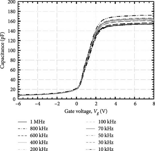
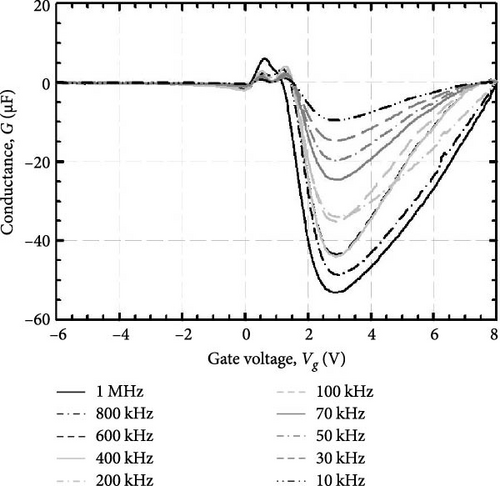
Additional information regarding the interface traps could be identified by employing high–low-frequency capacitance–voltage (C–V) and conductance techniques, whereby the interface state density (Nss) could be approximated by considering the frequency dispersion of conductance-voltage (G–V) and C–V characteristics recorded over a frequency spectrum ranging from 1 MHz to 10 KHz. The measured G–V and C–V curves were duly corrected, taking into consideration the series resistance (Rs) in order to eradicate the undesirable parasitic effects, thereby ensuring that the estimation of interface states could be rendered with precision [68]. The typically corrected C–V and G–V curves measured at different frequencies for the GaxCeyOz PL annealed at 900°C are presented in Figures 16 and 17, respectively. The subsequent equation was utilized to ascertain the Rs for the GaxCeyOz PLs that underwent postdeposition annealing at various temperatures in an N2–O2–N2 ambient [69]:
(9)
where ω is the angular frequency while Gma and Cma represent the measured conductance and capacitance values, respectively, in the strong accumulation region. The correction of the experimental G–V and C–V curves at different frequencies was carried out as per the determined Rs value (not shown) using the following equation [70]:
(10)
(11)
(12)
where Cc, Gc, Gm, and Cm denote corrected capacitance, corrected conductance, measured conductance, and measured capacitance, respectively. The high–low-frequency C–V method was also employed to determine the Nss for the investigated GaxCeyOz PLs, as expressed by the following equation [71]:
(13)
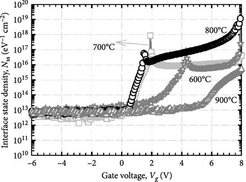
where CcLF is the lowest corrected capacitance value at a low frequency of 10 KHz while CcHF is the corrected capacitance value at a high frequency of 1 MHz that corresponded to CcLF. The calculated Nss values derived from the high–low-frequency C–V method as a function of Vg for the investigated GaxCeyOz PLs are presented in Figure 18. It was noticed that all of the GaxCeyOz PLs attained a comparable Nss during the application of negative bias. This observation was in line with the observed Qeff value wherein the acquisition of negative charges within the PLs could have occupied a deep level during the negative bias, contributing to the occurrence of charge trapping or detrapping at around the same rate for all of the investigated GaxCeyOz samples, and hence a comparable Nss value was observed. However, as the bias was shifted to positive, a significant dispersion in the Nss value was observed, suggesting that the response of traps against the bias could be significant during positive bias. This observation was consistent with the reported results that for a 4H-SiC-based MOS capacitor, in the accumulation region, all the traps could be filled with the majority carriers (electrons in this work) and responded quickly against the voltage bias [71]. Moreover, it was noticed that the GaxCeyOz PL annealed at 900°C attained the best interface quality in terms of a lower Nss value during the application of positive bias. This observation suggested that the passivation of Vo by the incoming oxygen ions, together with the passivation of Si and/or C dangling bonds by the nitrogen ions, could improve the interface quality as compared to other samples. Moreover, it has been noted that the PL of GaxCeyOz, which was annealed at a temperature of 600°C, has achieved the highest NssVg peak position at ~4.3 V. This indicated that the interface traps were positioned farther from the conduction band compared to the PL of GaxCeyOz annealed at 700°C (~1.84 V) and 800°C (~1.52 V). Nevertheless, the NssVg peak for the GaxCeyOz PL, which was subjected to annealing at 900°C, proved to be unattainable, thereby indicating the probable existence of border traps that are positioned in closest proximity to the conduction band. Consequently, it has been deduced that the elevation in the temperature of postdeposition annealing, which ranges from 600 to 800°C, has indeed contributed to the establishment of border traps that are situated farther from the conduction band. Furthermore, an observable degradation in the overall quality of the interface was noted for the GaxCeyOz PL when the temperature of annealing was increased from 600 to 700°C, which serves to further validate the hypothesis that this particular PL contains elevated concentrations of Vo, as well as unbonded nitrogen ions, both of which are likely to contribute to the formation of border traps that lead to a further degradation in the quality of the interface. Furthermore, it has been established that the GaxCeyOz PL specimen, which underwent annealing at 800°C, has attained the highest Nss value, thereby providing compelling evidence that a significantly greater concentration of nitrogen ions has been assimilated into this particular sample, and in this context, the nitrogen ions that have been incorporated are expected to function as border traps within the PL. The passivation of Vo by incoming oxygen ions in conjunction with the reoxidation of Ce3+ to Ce4+, as well as the passivation of Si and/C dangling bonds by the nitrogen ions at 900°C, which has led to the attainment of the best interface quality in terms of the lowest Nss value.
Details are in the caption following the image
Corrected capacitance–voltage measurements at different frequencies for gallium cerium oxide (GaxCeyOz) passivation layer (PL) at 900°C.
Details are in the caption following the image
Corrected conductance–voltage measurements at different frequencies for gallium cerium oxide (GaxCeyOz) passivation layer (PL) at 900°C.
Details are in the caption following the image
High–low-frequency Nss plot for gallium cerium oxide (GaxCeyOz) passivation layer (PL) at 600, 700, 800 [40], and 900°C.
Further, the Nss values calculated using the Hill–Coleman approach for the investigated GaxCeyOz PL could be represented by the following equation [72]:
(14)
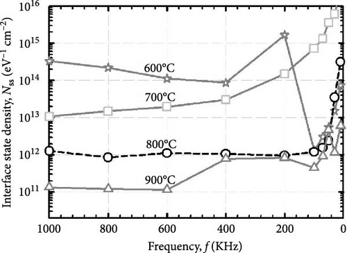
where is the peak value corresponding to the corrected Gc/ω–V curve, and Cc is the corrected capacitance corresponding to the . Figure 19 presents the calculated Nss values with respect to different frequencies ranging from 10 kHz to 1 MHz for the GaxCeyOz PLs subjected to postdeposition annealing at different temperatures in N2–O2–N2 ambient. It was observed from Figure 19 that the highest Nss value was observed for the GaxCeyOz PL annealed at 600°C, suggesting that this PL was composed of a higher concentration of defects, which had earlier led to the attainment of poor C–V and J–E characteristics. Furthermore, an enhancement in the quality of the interface, evidenced by a reduction in the Nss value, was noted as the annealing temperature was elevated to 700°C and beyond. Consequently, it was noted that the GaxCeyOz PL annealed at 900°C has attained the lowest Nss value, which was consistent with the high–low-frequency method. This observation further supported the hypothesis that the stimulated passivation of Vo by the impinging oxygen ions, together with the passivation of Si and/or C dangling bonds at this temperature, have contributed to the better interface between GaxCeyOz and the 4H-SiC substrate. Moreover, it could be noticed that at lower frequency ranges, a sudden increment in the Nss value was observed for the GaxCeyOz PL annealed at 700, 800, and 900°C, which made it obvious that at lower frequencies, interface states having a low time constant could follow the applied AC signal easily as compared to the high-frequency region, and hence a higher Nss value was observed at the low-frequency range. However, a sudden decrement in the Nss value was observed for the GaxCeyOz PL annealed at 600°C. The reason for this observation has yet to be identified. Moreover, it was worth mentioning that in this work, the observation of higher concentrations of STD and Qeff observed for the GaxCeyOz PL at 900°C has not contributed to the deterioration of interface quality, where reasonably low Dit and Nss were attained at this temperature, translating to good MOS characteristics.
Details are in the caption following the image
Hill–Coleman Nss plot for gallium cerium oxide (GaxCeyOz) passivation layer (PL) at 600, 700, 800 [40], and 900°C.

4. Conclusion

The formation of GaxCeyOz PL on 4H-SiC substrate following postdeposition annealing at various temperatures of 600, 700, 800, and 900°C in an ambient of N2–O2–N2 was presented. The successful doping of Ga3+ cation into the CeO2 crystal lattice to form the ternary GaxCeyOz PL has been confirmed by GIXRD, UV–VIS–NIR, as well as XPS measurements. It was found that nitrogen ions from the annealing ambient would plausibly attach to the Vo, generating additional Vo and/or diffused to the interface to passivate Si and/or C dangling bonds. It has been noted that at lower temperatures of 600 and 700°C, nitrogen ions primarily resided in the region of the GaxCeyOz PL to attach with the Vo. However, at higher temperatures of 800 and 900°C, the likelihood of nitrogen ions acquiring sufficient energy to diffuse to the GaxCeyOz/4H-SiC interface and formed attachments with Si and/or C dangling bonds increased. Consequently, the formation of the SiO2 IL was minimized at higher temperatures. Due to the increased doping of oxygen ions at higher temperatures of 800 and 900°C, the passivation of Vo was enhanced at these temperatures. Therefore, a superior J–E was observed at these temperatures, with an EB of 2.95 and 5.58 Mv/cm observed for the GaxCeyOz PL annealed at 800 and 900°C, respectively. Additionally, the higher ED and EID observed at higher temperatures of 800 and 900°C further confirmed that these PLs were composed of lower concentrations of Vo. XPS analysis confirmed that the Ce3+ state, in conjunction with the Vo, was minimal at the higher temperatures, with reoxidation of Ce3+ to Ce4+ being observed as the annealing temperature increased from 800 to 900°C. These observations were made in conjunction with the obtained k values of 24.11 and 24.01 for the GaxCeyOz PL at 800 and 900°C, respectively, with a minimal reduction in the k value at 900°C attributed to the slight increase in SiO2 thickness. Nevertheless, this study demonstrated that the impact of SiO2 thickness on the reduction of the k value was minimal. A further analysis of STD, Qeff, Dit, and Nss suggested that the GaxCeyOz PLs annealed at 800 and 900°C outperformed other samples in terms of performance, with the GaxCeyOz PL annealed at 900°C exhibiting optimum performance.

Conflicts of Interest

The authors declare no conflicts of interest.

Funding

The authors wish to express their gratitude for the financial assistance by the Ministry of Higher Education Malaysia through the Fundamental Research Grant Scheme (FRGS), referenced by Project Code: FRGS/1/2023/STG05/USM/02/8.

Acknowledgments

The authors wish to express their gratitude for the financial assistance by the Ministry of Higher Education Malaysia through the Fundamental Research Grant Scheme (FRGS), referenced by Project Code: FRGS/1/2023/STG05/USM/02/8.

    Data Availability Statement

    The data used to support the findings of this study are available from the corresponding author upon request.

      The full text of this article hosted at iucr.org is unavailable due to technical difficulties.