Novel AC–AC Converter Design for High-Efficiency Wireless Electric Vehicle Charging Systems
Abstract
Electric vehicle (EV) batteries may now be conveniently charged with wireless chargers. These systems are prized for their dependability and security in a range of weather scenarios. Generally speaking, there are two kinds of EV wireless charging systems: static (for parked cars) and dynamic (for moving cars). Traditionally, EV chargers have parts like a high-frequency direct current (DC)–alternating current (AC) converter that usually requires intricate cabling and an AC–DC converter that aids in power quality management. In these systems, a process called as “transformation” occurs when energy moves from a main component—the power source—to a secondary component—the vehicle’s receiver. Eliminating physical connections, such wires and charging outlets on the car, improves convenience and lessens wear and tear on the charger. This is another advantage of wireless chargers over plug-in varieties. In this study, we investigate a novel design that substitutes a single integrated AC–AC converter on the input side for the conventional AC–DC and DC–AC converters. This creative solution lowers the demand on power switches while raising voltage levels, which not only makes the system simpler but also more efficient. To further reduce the voltage stress on these switches, we additionally employ a multilevel diode clamp inverter, which not only helps to reduce the size of the switches but also greatly increases the efficiency of the system. To validate the performance of this new converter, we provide data from the laboratory as well as simulation results.
1. Introduction
More than ever, people are concerned about the depletion of fossil resources and the rising levels of air pollution. Consequently, more attention is being paid to the expanding use of fossil fuels in internal combustion engines [1]. Electric vehicle (EVs) are a suitable substitute for internal combustion engines to tackle these problems. These cars use the electricity in their batteries to provide kinetic energy instead of burning fuel or liquefied gas [2]. In addition, the adoption of EV has become more and more spurred by the rising expense of fuel [3].
Several factors make EV desirable, such as the depletion and growing price of fossil resources worldwide, the need to lessen environmental pollution, the fact that they produce less noise than vehicles powered by fossil fuels, and the fact that they are less expensive to operate than conventional vehicles [4]. In electric cars, the internal combustion engine is replaced by an electric motor, and a battery replaces the fuel tank. Batteries can be charged by off-grid electric sources like fuel cells, the vehicle’s regenerative braking system, and even grid connections. Fast start-up times, the ability to store kinetic energy when parked, almost zero pollutants, increased efficiency over gasoline-powered vehicles, no fuel usage, and low maintenance costs are just a few advantages of utilizing EV [5]. The drawbacks include reliance on batteries, a restricted operating range because of battery capacity, poor acceleration, a substantial weight penalty, and expensive starting expenses [6].
Assessing the effectiveness and suitability of various charging methods becomes essential as the shift to EV increases. These challenges are prompting scientists to look into alternative EV power sources. Scientists are investigating different ways to power EV due to these difficulties. One approach to providing energy is to use wireless power transmission (WPT). The users can send power ranging from several watts to tens of kilowatts via WPT, sometimes called contactless and magnetic coupling power transfer. This technology is highly dependable, safe, and practical. Water, chemicals, snow, and pollution do not affect WPT [7].
But even with these benefits, wireless charging methods have some significant drawbacks. Significant limitations include lower efficiency and greater starting expenses when compared to traditional plug-in chargers. Furthermore, even though WPT systems are usually safe, adverse weather or other environmental circumstances may have an impact on how well they function and how safe they are [8]. It is critical to support safety claims with particular research or technological modifications that deal with these issues. For example, to reduce such impacts and improve the operational safety and efficiency of WPT systems in different environmental circumstances, sophisticated shielding and adaptive control systems have been developed [9].
Table 1 offers a thorough comparison of aspects like convenience, charging speed, safety, energy efficiency, and environmental effect to highlight the advantages and disadvantages of wireless charging over conventional plug-in techniques.
| Feature | Wireless chargers | Ref | Plug-in chargers |
|---|---|---|---|
| Convenience |
|
[9] | - Requires manual connection, which can be inconvenient in adverse weather or tight spaces |
| Charging speed |
|
[10] | - Faster charging capabilities, especially with DC fast chargers (up to 350 kW) available |
| Safety |
|
[8] | - Safety risks associated with exposed connectors in wet conditions |
| Energy efficiency |
|
[11] | - High efficiency, often above 95%, especially in DC fast charging systems |
| Installation cost | - Higher initial infrastructure costs due to the need for specialized equipment and installation | [12] | - Generally lower installation costs; widespread availability of plug-in stations |
| User experience |
|
[13] | - Familiar and straightforward for users but can be cumbersome for frequent charging |
| Maintenance |
|
[6] | - Established technology with known maintenance requirements; issues typically arise from wear and tear on connectors |
| Environmental impact |
|
[14] | - Emissions depend on the energy source; renewable integration is crucial for minimizing environmental impact |
- Abbreviations: AC, alternating current; DC, direct current; EVs, electric vehicles.
Hidayah, Suryoatmojo, and Pamuji [15] investigated using a single-phase matrix converter in WPT to charge EV in parking lots. In line with global trends toward greener technology, this work introduces a novel resonant inductive coupling method that significantly improves the safety and practicality of EV charging. Vinod et al. [10] emphasized using primary side control techniques in EV applications when focusing on battery charge management in WPT systems. The paper compares and contrasts several control approaches to maximize charging process stability and effectiveness. Their research advances our knowledge of how precise control may boost WPT system efficiency, which directly increases the dependability of EV charging. In their critical analysis of modern power electronics interface topologies for renewable energy integration, Tasnim et al. [16] highlighted how they might improve and stabilize power quality. Although not limited to EVs, the topic of interface topologies is relevant to any WPT application where effective energy transfer is essential, including EVs. Because of its increased power density compared to other WPT methods, inductive power transmission (IPT) is utilized explicitly in EV [17]. IPT has low magnetic inductance; hence, both the primary (transmitter) and secondary (receiver) sides require adjustment. These techniques allow energy to be transferred without requiring a physical electrical connection, which frees the EV from needing to travel a predetermined path. There are no related mechanical connection issues because there is not a mechanical connection between the grid and the vehicle [18]. This method keeps batteries as energy storage devices rather than removing them entirely from the electric car system. They are smaller, less volumetric, and receive sporadic charging using contactless techniques [19].
A fault-tolerant multilevel inverter, invented by Zhang et al. [20], is needed for applications such as IPT systems where continuous operation is required. It is designed to retain output integrity under fault conditions. Their application of cutting-edge modulation techniques to lower power losses and boost efficiency is similar to the optimization methods we employ in our IPT research on electric cars. The objectives of our study to guarantee dependable and continuous EV charging are directly supported by this work, which provides significant insights into attaining robustness in IPT systems. Zhou et al. [21] devised a spread-spectrum modulation technique to minimize electromagnetic interference (EMI) in multiphase indirect matrix converters. This technique is very significant in reducing EMI in EV IPT systems. Their emphasis on improving power conversion efficiency and the harmonic spectrum aligns with our research’s goal of maximizing system safety and energy transfer efficiency in IPT-based EV charging. Their practical demonstration of less EMI and better waveform quality provides applicable standards for us to advance IPT technology in our study.
Series–series (S/S), series–parallel (S/P), parallel–series (P/S), parallel–parallel (P/P), and mixtures of series and parallel tanks, such as LCL and LCLC, are examples of several types of compensation networks [22]. In compensatory networks, S/S and S/P arrangements are frequently employed, although P/S and P/P tanks are less often used because of load-dependent escalation [11, 23]. In IPT applications, it is typically required to set the switching frequency at the resonant frequency of the resonant tank to guarantee that the power converter circuit receives the minimal amount of volt-ampere (VA), which lowers power loss and reduces converter size [12]. The majority of compensator networks employed on the primary side are series and have an LCL structure [24]. An LCLC tank is created when an extra capacitor is occasionally added to the LCL tank in series with the coil to improve system performance [13].
Ali et al. [25] examined the enhanced passive damping design for single-phase grid-connected LCL-filtered inverters. Since the concepts they cover can be utilized to lower harmonic distortion and improve the power quality in systems used to charge electric cars, their work is vital to any application utilizing WPT. The article [14] discusses optimizing a resonant inductive power transmission (RIPT) system for charging the battery banks of EV. This study assesses a RIPT system for light car charging and provides diagrams to clarify the system’s operational characteristics. The results indicate that the resonant frequency should be between 25 and 51 kHz, and the inductance coefficient of the coil should be between 111 and 151 µH for the best possible resonant WPT system design.
Despite these developments, there are still fundamental inefficiencies in the wireless charging solutions available today, which our study seeks to resolve. A few of these are the hefty infrastructure expenses related to charging, the sluggish energy transfer speeds, and the significant energy losses that occur throughout the process [26, 27]. By utilizing state-of-the-art technology, our research presents a revolutionary IPT system that addresses these particular problems and enhances the efficiency, accessibility, and affordability of EV charging infrastructure.
The design and assessment of a high-efficiency WPT system will be covered in this talk, emphasizing the novel alternating current (AC)–AC converter design. By directly converting AC from one waveform to another, this technology increases power density and streamlines the system design as a whole. Conventionally, systems use two stages—AC–direct current (DC) and DC–AC conversion—to convert AC to DC and back to AC. By eliminating these intermediary stages, our design lowers operating costs and energy losses. We also present a new component, a multilevel diode clamp inverter. This sophisticated inverter, in contrast to traditional inverters, improves system efficiency by precisely controlling electrical flow, which also makes smaller power switches possible. These developments show their efficacy in practical situations and indicate their potential for wider application. They are backed by solid modeling and empirical evidence.
In this article, an attempt is made to design an IPT system for wireless charging of EV, focusing on the power electronics part of this system. The main goals of this research are to design an induction power transmission system with high efficiency and its simulation by MATLAB/Simulink software and to implement a laboratory sample to provide a solution to improve the prosperity of this industry.
- •
Innovation in design: A revolutionary development in wireless charging technology, this integrated AC–AC converter efficiently raises voltage levels while decreasing current stress on power switches.
- •
Enhanced system efficiency: The implementation of a multilevel diode clamp inverter markedly improved efficiency and reduced the size of power switches, signifying a major enhancement compared to conventional systems.
- •
Validation through testing and simulation: Strong simulation and empirical data from lab samples were provided, supporting the suggested system’s practical viability and performance promises.
- •
Strategic directions and improvements for next-generation wireless charging systems were outlined, to stimulate additional research and development in this vital field of electric car technology.
The remainder of the paper is as follows: The background information on wireless chargers and electric cars is covered in the second section, which also sets the scene for the advances that are presented. The architectures of isolated, nonisolated, and wireless charging systems are presented in the third section to improve comprehension of various integration strategies. The framework of our innovative wireless charging system, complete with comprehensive design schematics, is introduced in the fourth section, marking a significant advancement in the integration of charging technologies. In the fifth section, we show the efficacy and operational efficiency of the suggested system by validating it with simulation results and lab testing. The last section provides a thorough synopsis, broad conclusions, and recommendations for the future based on our research.
2. The Structure of the Proposed Wireless EV Charger
This article proposes a wireless EV charger system based on the dual LCC series structure to increase the DC link voltage and remove the diode bridge. In the proposed structure, the power switches’ current is reduced by using a voltage-increasing circuit. Also, to reduce the voltage stress of the power switches, the diode clamp inverter was used, which reduced the size of the switches and increased the efficiency of the proposed converter.
The proposed system consists of a high-frequency AC–AC converter, an LCC compensator, and a rectifier for battery charging. Figure 1 shows the proposed system’s circuit structure. Figure 1a shows that a single-stage AC–AC converter generates high-frequency AC voltage from the AC input source. The inductor at the input, together with the power switches, acts as a conventional boost converter and increases the input voltage with a gain of (D is the duty cycle of the power switches). Also, the capacitors are DC link capacitors, and their values are much larger than the resonant capacitors, so they will not have an effect on the resonant circuit performance.
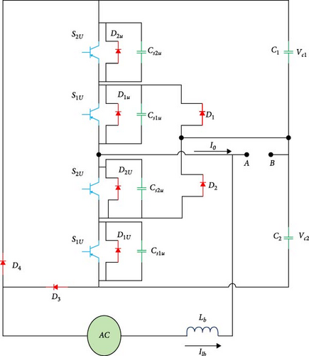

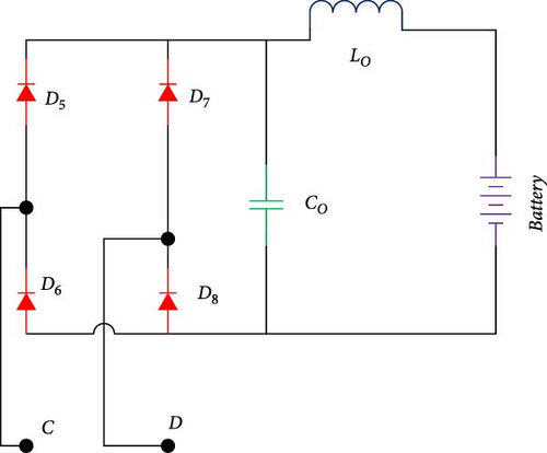
The output of the inverter in Figure 1a is a high-frequency AC voltage. The resonance circuit and the air-gap transistor transfer the input source energy to the secondary side of the transformer, which is connected to the rectifier coupled to the battery. Finally, the energy transferred to the secondary through fast rectifier diodes is rectified and charges the battery. The following presents the analysis and operation of each part of the wireless EV charger system.
2.1. The Suggested Inverter’s Structure
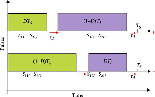
Figure 1a depicts the inverter’s construction as presented in this article. The average value of the input AC voltage following the diode bridge is equal to Vin, which is used to construct the inverter and establish the nominal values of its semiconductor elements. This article uses a resonant type of inverter. Resonant converters are used because they transmit higher powers, have a high conversion efficiency, produce soft switching, and eliminate switching losses. Figure 2 illustrates the suggested inverter’s switching mechanism and how the switches are pulsed during the input voltage’s positive and negative half cycles. This converter’s output voltage can be adjusted by pulse width modulation or switching frequency control. It should be remembered when pulsing the keys that 50% is the maximum duty cycle (D) that can be used to regulate this converter, independent of dead times.
2.2. Working Fashions
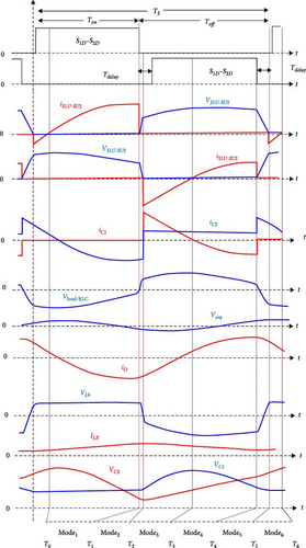
Considering that the DC link capacitors do not interfere on the resonance circuit and their values are much larger than the resonance capacitors (at least 10 times larger), these capacitors are used as a DC link with an increased voltage of () which are equal to the average value of the input voltage (Vin) after rectification. Also, considering the resonant compensation system and the rectified resistive load as an RLC resonant tank that work at a frequency higher than the resonant frequency, the modes of the operation of the proposed circuit along with the voltage and current waveforms of some key elements of the circuit are shown in Figure 3.
2.3. Working Modes of the Proposed Converter in the Positive Half Cycle of the Input
Considering the positive half cycle of the input voltage, different current paths and working modes are created during a switching period. These work modes are discussed as follows.
2.3.1. The First Work Mode
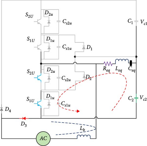
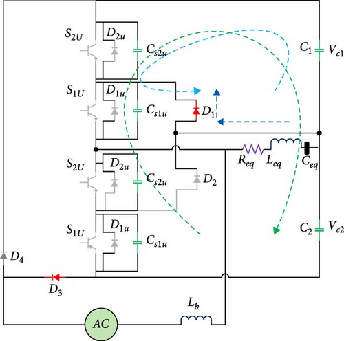
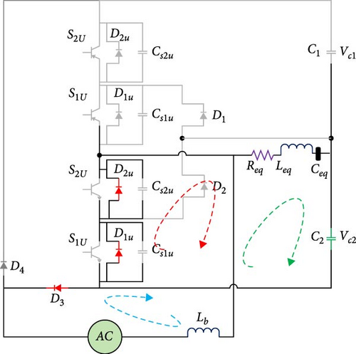
As seen in Figure 4a, in this mode, the lower leg keys of the inverter receive pulses and are turned on. The capacitor C2 is discharged, and the input inductor is charged. Also, the resonant capacitor Ceq is also discharging. It should be noted that the capacitor Ceq is charged in the sixth mode that occurs before this mode.
2.3.2. The Second Method
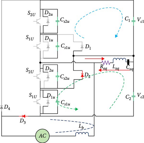
Considering that at the moment when the lower keys are turned off, the external snubber capacitors of the keys have zero voltage, so the keys are turned off in the form of zero voltage switching (ZVS). Also, in this mode, the external snubber capacitors of the upper leg power switches are discharged, and before turning on the keys, the voltage on them reaches zero. In other words, it prepares the upper keys to be turned on as ZVS. The positive half cycle of the second working mode is shown in Figure 4b.
2.3.3. Third Operating Mode
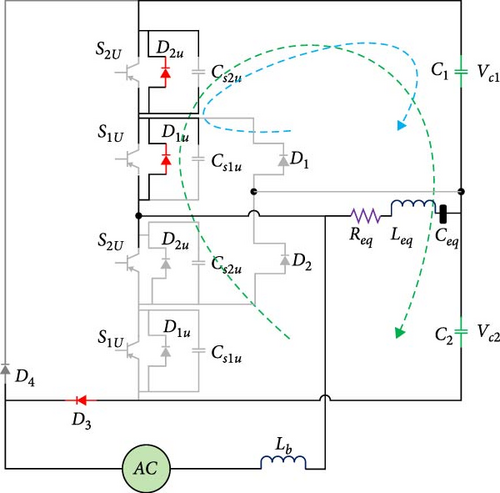
As can be seen in Figure 4c, in this mode, the inverse parallel diodes related to the upper leg switches are conducted, and in addition to the zero voltage of the switches, the current passing through them also reaches zero. Therefore, after this working mode, the power switches will be turned on as ZVS and zero current switching (ZCS). Also, the DC link capacitors are charged through the inductor Lb and the input source; as a result, the inductor Lb is discharged.
2.3.4. Fourth Operating Mode
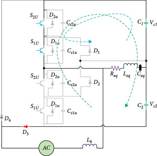
As seen in Figure 4d, in the fourth working mode, capacitor C2 is still charging, and capacitor C2 starts discharging on the load through the upper leg switches. In addition, the input inductor is discharged on the load and capacitor C2 and increases the output voltage.
2.3.5. Fifth Operating Mode
In the fifth method, as seen in Figure 4e, the capacitor C1 is discharging on the external snubber capacitors of the upper leg switches, and by increasing their slow voltage, it causes the power switches to turn off in ZVS mode. Also, by discharging the external snubber capacitors of the lower leg keys, the conditions for turning on the ZVS of the said keys are provided.
2.3.6. Sixth Grade
In this working mode, the booster inductor is still discharging and leads to the charging of capacitor C2. To continue the amplification process, diodes in reverse parallel with the lower leg switches are forced on and lead to zero current in the power switches before they are turned on. As happened in the previous mode, the voltage of the power switches has already gone to zero. Therefore, the lower leg power switches are turned on in the ZVS–ZCS state. Also, in this interval, the voltage of capacitor C1 remains constant, and the power switches of the upper leg are still off. The positive half cycle of the sixth working mode is shown in Figure 4f.
2.4. Working Modes of the Proposed Converter in the Positive Half Cycle of the Input
2.4.1. The Initial Operational Mode
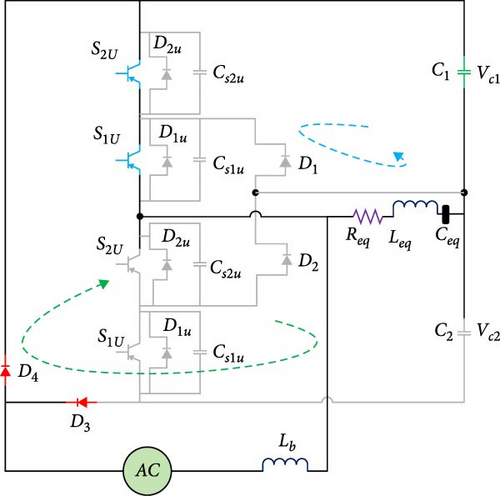
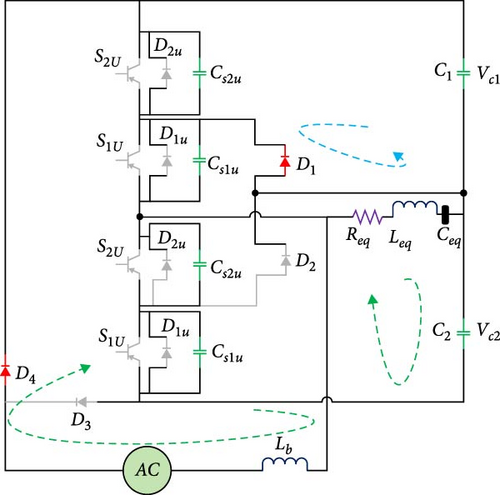
Figure 5a illustrates how the input current route is closed through the diode D4 during the input voltage’s negative half cycle. In contrast, diode D3, which was always on during the positive half cycle, is always off during this half cycle. Firstly, the input inductor is charged through the two upper leg keys, which are switched on. Additionally, the load causes the capacitor C1 to discharge. The reverse parallel diodes of the keys are off, and the voltage of the capacitor C2 stays constant when the key is in this operational mode.
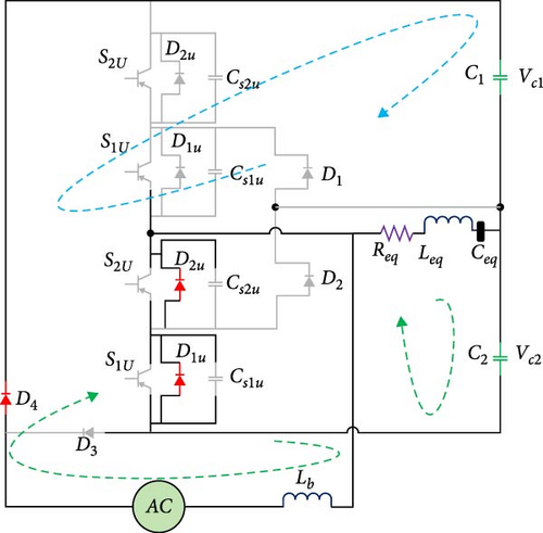
2.4.2. Second Working Mode
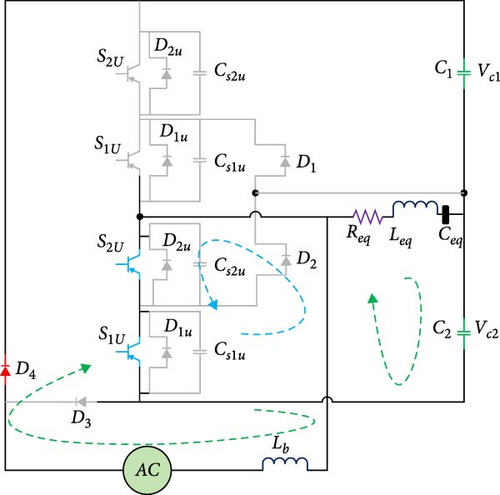
According to Figure 5b, in this method, the power switches of the upper leg are turned off, and the external snubber capacitors parallel to them are slowly charged and ensure the switch off under zero voltage (ZVS). Also, in this working mode, all the power switches are turned off, and the external snubber capacitors of the lower leg, by discharging themselves, prepare the conditions for turning on the power switches at zero voltage for the next working modes.
2.4.3. Third Working Mode
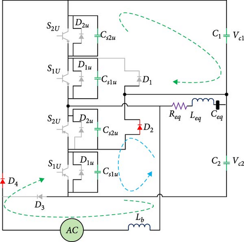
According to Figure 5c, in the third working mode, the resonant load is still completing its resonant process in the positive direction, and the amplifier inductor (Lb) is discharged on the DC link capacitors (C2 and C2). Also, because in the next mode, the power transistors of the lower leg will be turned on; the diodes D1d and D2d will start to conduct so that the current of the keys is equal to zero when they are turned on. In other words, the ZVS–ZCS conditions are fully established for the keys to be turned on in the next working mode.
2.4.4. Fourth Grade
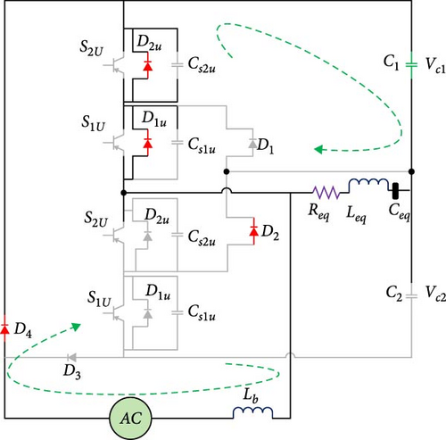
As seen in Figure 5d, in this mode, the lower leg switches of the inverter are turned on under soft switching and in ZVS–ZCS conditions. Also, the capacitor C1 is being charged and is preparing to complete the intensification process in the next working modes. Also, the resonant load is fed through the capacitor C1 and the inductive current. In this working mode, the direction of feeding the load is also changed, and it remains like this for the next several working modes so that by creating an alternating voltage in the two ends of the resonant load, it can induce a voltage in its secondary side. This induced voltage will be used to charge the battery after rectification.
2.4.5. Fifth Working Mode
This method is similar to the second method. Of course, with the difference that this time, the zero voltage conditions are provided for the lower power switches to turn off as ZVS. Also, at the same time, the zero voltage conditions are provided for the upper leg switches before turning on. The negative half cycle of the fifth working mode is shown in Figure 5e.
2.4.6. Sixth Working Mode
The inverse parallel diodes of the higher leg switches are activated in this mode, as shown in Figure 5f, and they set the circumstances for the upper leg switches to switch on under zero current before being turned on. The S1U and S2U switches are turned on under the soft switching method and with ZVS–ZCS circumstances in the next operating mode, which is the same as the first mode.
The compensating circuit’s resonant frequency in Figure 1b is the same as the resonant frequency for the resonant load. In order for the circuit to function in the self-locking zone, the output voltage and current frequency must also be equal to the switching frequency and consistently higher than the circuit’s resonance frequency.
3. Necessary Conditions for Establishing ZVS With the External Snubber Capacitor of the Keys
3.1. LCC Compensation System
To transfer energy through the air gap (the distance between the vehicle charging system and the resonant circuit of the charger side), the compensating system of Figure 6 is used [28].

The parameters used in LCC are given in Table 2.
| Characteristic | Parameter | Characteristic | Parameter |
|---|---|---|---|
| The first-order RMS value of the input voltage | uAB | First-order phasor of the input voltage | UAB |
| The first-order RMS value of the output voltage after rectification | uCD | First-order phasor of output voltage before rectification | UCD |
| Inductance of coupled inductor | M |
As it is clear from the above relationships, the resonant frequency depends only on the values of the inductor and capacitor of the resonant circuit and has nothing to do with the load conditions and the coupling method. Also, by using this LCC structure, by increasing the mutual inductance, the transmitted power to the output increases, and by decreasing it, the amount of output power decreases. This means that the amount of power transmitted will increase as the vehicle approaches the charger coil. Of course, it is certain that there will be a minimum distance between the primary winding and the existing winding on the vehicle. Also, using Equations (3)–(6) for output power, it can be seen that factors such as resonance frequency and inductances Lf1 and Lf2 as well as input and output voltages are effective in transmission power.
Using relations Equations (3)–(5) and Equations (3)–(6), it can be seen that the input voltage and current of the compensator are in phase. Therefore, the unit power factor is obtained by the compensator system.
3.2. Rectifier System and Output Filter
As seen in Figure 1c, the alternating voltage output of the LCC compensator enters the rectifier circuit and is connected to the battery through an LC filter. The diodes used in this circuit must be of the fast type and the inductor and capacitor. Filters are used to remove current and voltage ripple.
3.3. Design of Inductor
In order to clarify the calculations and calculate the impedance of the circuit in relation to the design of the inductor, a coefficient called ripple-factor (γ) is defined which is equal to the following:
3.4. Designing Circuit Parameters of Compensator
3.5. Proposed Converter Control System
To control the proposed converter, a closed loop control system with a PI controller has been used.
The proposed control system for the circuit is shown in Figures 7 and 8.
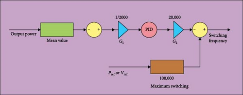

The basis of the work is that the controller should be able to control the switching frequency between 80 and 100 kHz. In the control system presented in Figure 7, the desired power is given to the system as a reference, then through a PI controller and fixed gain blocks, a signal is produced that is proportional to the switching frequency. The control signal created by control diagram block is given to the pulse generator block according to Figure 8 to create the gate signals of the keys.
Also, to control the output voltage, Equations (3)–(8) can be used, and the output current can be fixed at the desired value by controlling the input voltage. Since the output voltage is equal to the product of the output current multiplied by the constant value of the output resistance, therefore, by controlling the output current, the output voltage is also controlled.
3.6. Output Equivalent Circuit From Inverter Point of View
3.7. Winding Design
4. Simulation
In this section, in order to show the capabilities and confirm the performance of the proposed converter, the simulation results and the results of the experimental sample of the proposed converter in Figure 1a–c are presented and reviewed.
The simulation results have been obtained using MATLAB software and Simulink environment. The values and parameters used in the simulation for the proposed converter elements are presented in Tables 3–5:
| Characteristic or element | Value |
|---|---|
| Vac | 220 Vrms–50 Hz |
| Lb | 500 μH |
| Cs1u − Cs2u − Cs1d − Cs2d | 33 nF |
| C1 − C2 | 1 μF |
| fs | 85 kHz |
| RO output load | 100 Ω |
| Characteristic or element | Value |
|---|---|
| Lf1 − Lf2 | 116 μH |
| Cf1 − Cf2 | 33 nF |
| C1 − C2 | 15 nF |
| L1 − L2 | 360 μH |
| M mutual inductance | 100 μH |
| Characteristic or element | Values |
|---|---|
| Lo | 100 μH |
| Co | 1000 μH |
| Ro | 100 Ω |
In the simulation, a 100 Ω resistor is used instead of a battery. Also, the output voltage of the DC side is equal to 240 V.
4.1. Simulation Results of the Proposed Wireless Charging System
The simulation results of the proposed converter for a load of 650 W at the output are presented in this section. During the simulation, the duty cycle is constant at 40%, and the switching frequency is equal to 85 kHz. Also, the dead time between the pulses of the upper and lower leg switches of the inverter is considered equal to 1 µs. The waveform of the pulses applied to the gate related to the power switches S1U − S2U − S1D − S2D is shown in Figure 9.
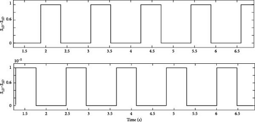
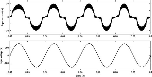
As can be seen in Figure 9a, the gate pulses of the upper and lower leg switches of the inverter have a phase difference of 180°, and a dead time interval (Tdelay) is applied between these pulses so that the upper and lower leg switches under no circumstances do not turn on at the same time. Also, to complete the soft switching function by using the snubber capacitors on the power switches, the presence of this delay time is necessary. Considering that the input voltage of the proposed charger system is directly connected to the city electricity with a voltage of 220 V and a frequency of 50 Hz, the presence of current with a suitable quality and in phase with the input voltage can be effective in determining the quality of the current drawn from the network. For the proposed converter under simulated conditions, the waveform of voltage and input current can be seen in Figure 9b.
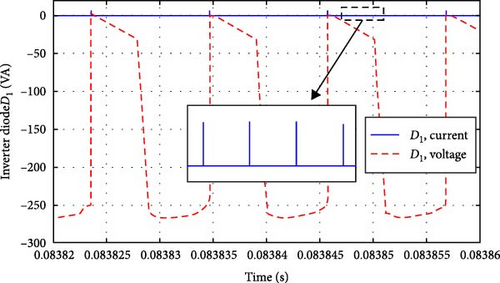
The current and voltage waveforms of diodes D1 to D4 of the inverter section of the proposed converters are shown in Figure 10a–d. The current of diodes D3 and D4 is equal to the input current from the city electricity side. Diode D3 conducts in positive half cycle, and diode D4 conducts in negative half cycle. As can be seen, diodes D1 to D2 conduct when the lower leg snubber is activated. Also, diodes D3 and D4 operate in positive and negative half cycles, respectively, and create the current conduction path in positive and negative voltage half cycles.

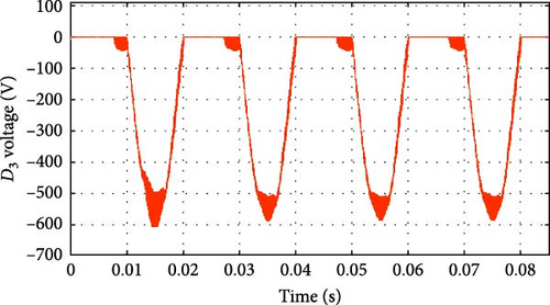
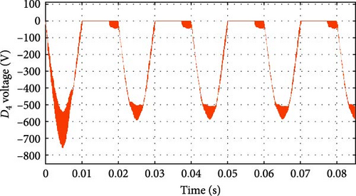
To show the soft switching performance of the proposed converter power switches according to the working modes mentioned in the previous section, the voltage and current waveforms of the S1U − S2U − S1D − S2D switches are shown in Figure 11a–d.
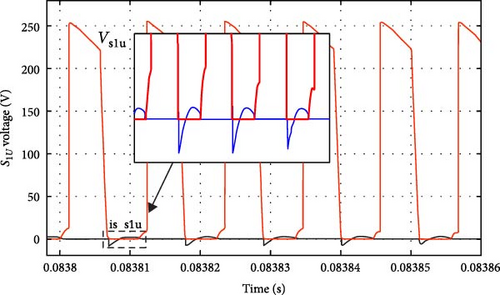
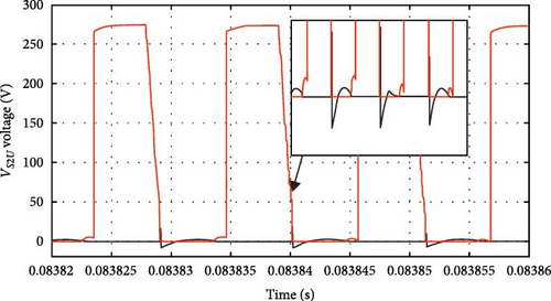
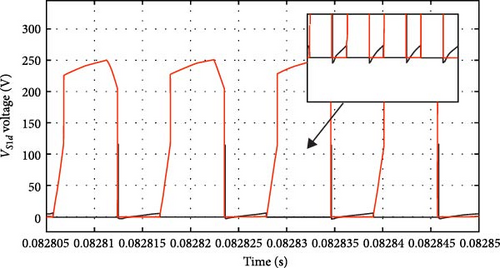
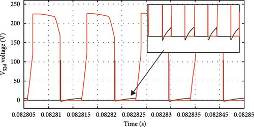
As seen in Figure 11a, the power switch is turned on as ZVS–ZCS and turned off as ZVS. Also, the voltage range of the power switch is equal to the product of half the input voltage and the gain of the boost converter. The occurrence of soft switching in power switches causes a significant reduction in switching losses, and the majority of losses in the proposed converter are caused by the conduction losses of diodes and switches.
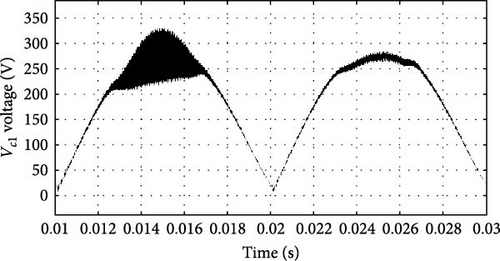
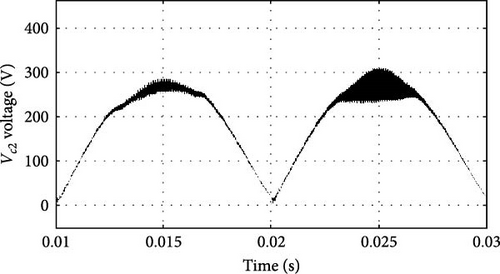
The voltage of capacitors C1 and C2 is shown in Figure 12a,b, respectively. Figure 12b shows voltage waveform of capacitor C2 in a cycle of input voltage. Also, the voltage waveform of DC link, which is equal to the sum of voltages of capacitors C1 and C2, is presented in Figure 12c. The waveform of the output voltage of the inverter is a high-frequency alternating voltage whose amplitude increases or decreases according to the switching frequency and duty cycle. The output voltage’s detailed waveform, depicted in Figure 12d, illustrates how operational alterations have an instantaneous impact. On the other hand, Figure 12e shows the range of these output voltages under various operating circumstances, emphasizing the inverter’s response over a wider range of parameters. For the current passing through the inductors Lf1 and Lf2 in the compensating system of Figure 1b, Figure 13a–c is presented. Additionally, these figures indicate stable and controlled voltage and current behaviors, characteristic of reduced stress on the system components due to the integrated design.
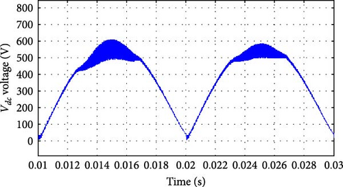
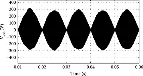
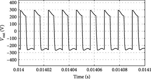
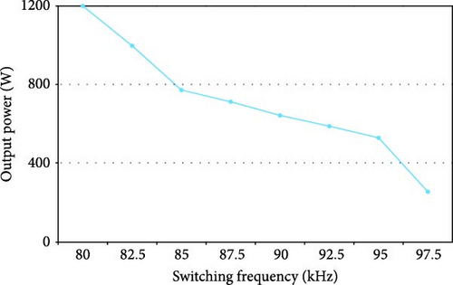
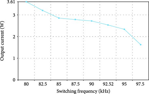
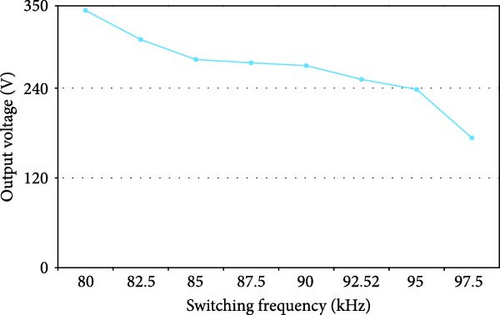
Due to the ability to control the output power by changing the switching frequency in the range of 80–100 kHz, it is possible to control the output power by changing the switching frequency. In series RLC circuits, as the frequency increases from the resonance frequency, the load impedance increases, and the output power and current decrease. The following figures show the changes in output power, current, and voltage according to changes in the switching frequency.
4.2. Checking the Performance of the Proposed Converter Control System
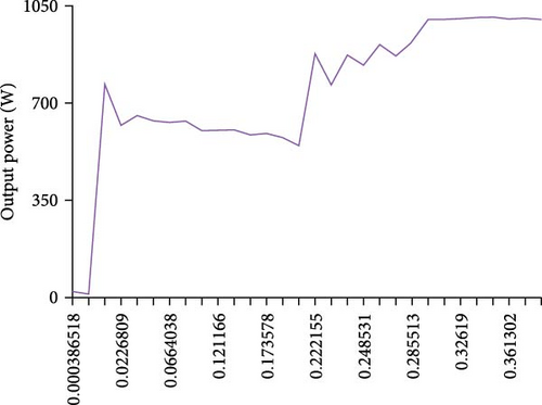
In order to check the dynamic behavior and correct operation of the control system presented in Figure 14a for the proposed converter, the output power reference value is changed step by step at the moment t = 0.4 s from 600 to 1000 W. Figure 14a shows the changes in the output power under the above conditions. As can be seen in this figure, it has been able to bring the output power value to its reference value in a period of about 100 milliseconds.
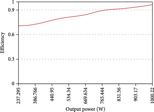
The efficiency of the proposed converter per load change from 400 to 1900 W is shown in Figure 14b. As it is known, the maximum efficiency has been obtained in the power of 1900 W and equal to 96.5%. As the output power decreases due to the dominance of switching losses over conduction, the efficiency of the converter decreases further. To achieve higher powers, a mutual inductance of 200 μH is included. From Figure 14, particularly Figure 14b which illustrates the efficiency curve across different output powers, it is evident that the integrated AC–AC converter achieves high efficiency. The maximum efficiency noted at higher powers indicates effective management of energy, likely translating into lower stress on system components over time.
The results of the simulation for different circuit elements as well as their functional modes are consistent with the items mentioned in the previous section, and according to the items mentioned in the previous section, changes in the current and voltage of the elements have occurred.
5. Laboratory Sample Results
This section uses comprehensive laboratory tests to validate the accuracy and show the capabilities of the proposed converter. The elements are redesigned to operate optimally at a resonance frequency of 21 kHz, reflecting the modifications required by the frequency limitations of the TLP250 (IGBT) drivers. A thorough examination of the modified converter components is included below, along with the practical results of these testing.
5.1. Design and Parameters of the Converter
5.1.1. Inverter Section (Figure 1a and Table 6)
To improve durability and performance under higher operating demands, the inverter’s operational specifications include a 100 Vrms input at 50 Hz, power switches (FGH 60N60), and diodes arranged in triples (4007 μF).
| Characteristic or element | Values |
|---|---|
| Vac | 100 Vrms–50 Hz |
| Lb | 740 μH |
| Cs1u − Cs2u − Cs1d − Cs2d | 33 nF |
| C1 − C2 | 2.2 μF |
| fs | 21 kHz |
| Power transistors | FGH 60N60 |
| Diodes | 4007 μF−3 to parallel (instead of each diode) |
5.1.2. Compensator Section (Figure 1b and Table 7)
The compensator, which uses precisely tuned inductors (Lf1 and Lf2) and capacitors (Cf1, Cf2, C1, and C2) to manage the power flow and quality across the system accurately, is essential to preserving system stability and efficiency.
| Characteristic or element | Values |
|---|---|
| Lf1 − Lf2 | 230 μH |
| Cf1 − Cf2 | 560 nF |
| C1 − C2 | 500 nF |
| L1 − L2 | 360 μH |
5.1.3. Output Section (Table 8 and Figure 1c)
A 100 Vdc output voltage across a 250 Ω load is one of the output characteristics that are crucial for assessing the converter’s practical application since it shows the converter’s capacity to maintain a steady output even when under load.
| Characteristic or element | Values |
|---|---|
| Lo | 100 μH |
| Co | 470 μF |
| Ro | 250 Ω |
| Vo | 100 Vdc |
Figure 15 shows the overview of the implemented wireless inductive power transmission system.

5.2. Crucial Performance Findings
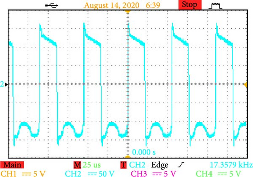
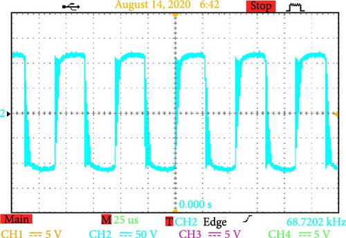
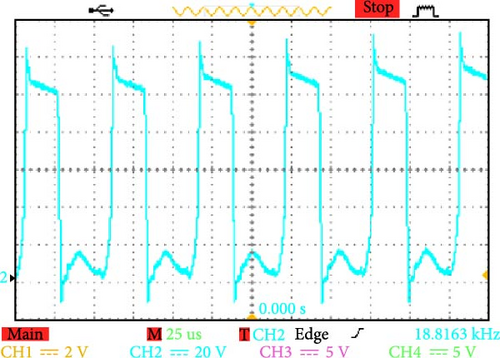
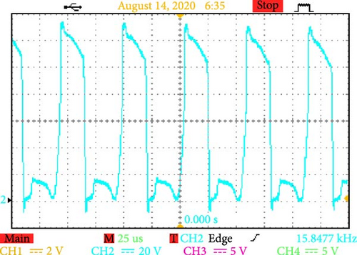
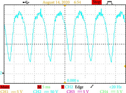
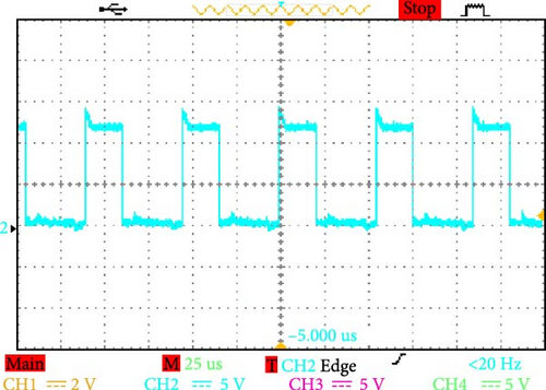
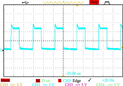
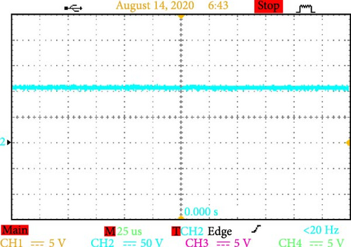
5.2.1. Dynamics of Voltage Waveforms (Figures 16a–d and 17a–d)
The converter can efficiently manage alternating voltage ranges, as evidenced by a detailed examination of the voltage across terminals AB and CD. It can also increase the working voltage in the DC connection to as high as 300 V (Figure 17a). These dynamics demonstrate how well the converter handles high-power applications and how resilient it is to operational stressors.
5.2.2. Charge Dynamics and System Efficiency (Figure 18a–d)
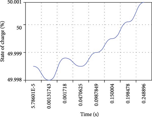
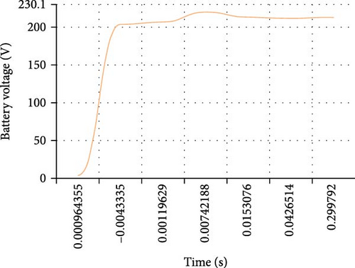
An evaluation is conducted on the converter’s performance under constant voltage and constant current charging conditions. The converter effectively controls the charging process, ensuring constant current and voltage levels for a battery with a capacity of 50 A.h and a full charge voltage of 215 V, as shown by Figure 18a–d. This demonstrates how well the system works in practical energy storage applications.


The laboratory assessments greatly improve our knowledge of the practical applications of the proposed converter by confirming its high efficiency and dependability. These outcomes validate the design improvements made to the converter and show its potential in commercial and industrial environments where reliability and effectiveness are critical. The laboratory data have been succinctly and clearly summarized in this part, which has been extended in response to prior requests for a more thorough and persuasive presentation of our results.
6. Conclusion
- 1.
Reducing the voltage stress of the input inverter switches
- 2.
Reducing the current of the power switches for constant output power compared to the half-bridge inverter without boost mode, due to the voltage increasing function
- 3.
No need for an input diode bridge
- 4.
High efficiency
While this work was on the power converter front of inductive EV charging, it does not fully realize real-world scenarios of variable magnetic coupling or coil geometrical issues. Optimization of inductor designs and their configurations is a suggested future work for realistic misalignment/coupling situations. Further work on increasing the scope to more integrated system analysis, looking into alternative inverter structures, and switching strategies will further improve the efficiency and scalability of the system.
Conflicts of Interest
The authors declare no conflicts of interest.
Funding
No funding was received for this research.
Open Research
Data Availability Statement
The data that support the findings of this study are available from the corresponding author upon reasonable request.


