Effect of Gamma-Ray Irradiation of Amorphous SnO2 Electron Selective Layers on the Properties of Ambient-Air Synthesized Planar Perovskite Solar Cells
Abstract
The effect of low-dose gamma-ray irradiation on an amorphous SnO2 electron-selective layer (ESL) was investigated in this study. Further, its impact on the photovoltaic (PV) performance of planar perovskite solar cells (PSCs) based on MAPbI3 and CsFAMAPbIBr absorber layers has been evaluated for the first time. The properties of the SnO2 layer were substantially modified by the gamma-ray irradiation of regulatory exemption radioactive sources (Co-60). Gamma-ray irradiation promoted the formation of large perovskite grains by creating a hydrophilic surface via the generation of ─OH on the amorphous SnO2 film surface. In addition, gamma-ray irradiation increased the conductivity of the SnO2 layer due to the generation of the proper oxygen vacancies in SnO2. From the optimization of gamma-ray irradiation parameters, we achieved a best efficiency of 18.03% using the MAPbI3 perovskite film owing to the enhanced perovskite densification and increased SnO2 conductivity. This efficiency was significantly improved compared to that (16.03%) of a pristine device. In addition, a power conversion efficiency (PCE) of 20.01% was achieved using the CsFAMAPbIBr mixed perovskite film and the gamma-ray irradiated SnO2. The results suggest that systematic low-dose gamma irradiation treatment of ESLs has a synergistic effect of controlling surface properties, enhancing perovskite crystal growth, and controlling oxygen vacancies, and is relatively simple and has high potential as a surface treatment process.
1. Introduction
Perovskite solar cells (PSCs) are receiving widespread attention as their power conversion efficiency (PCE) has rapidly increased in a short period from 3.8% in 2009 to a current world record of 25.5% [1–3]. Typically, PSC has a planar-heterojunction (PHJ) structure in which the perovskite absorber film acting as a carrier generator is sandwiched between a p-type hole-selective layer (HSL) and an n-type electron-selective layer (ESL) [4]. In a PHJ PSC, ESL plays an important role in promoting the separation and extraction of excited electrons from the perovskite absorption layers. To date, diverse n-type metal oxides, such as TiO2 [5], SnO2 [6], Zn2SnO4 [7], and In2O3 [8] have been used as an ESL in the PSC device architecture. An ideal ESL for highly efficient PSCs should have basic requirements, including suitable energy bandgap, high optical transmittance, high electron mobility, low carrier trap density, and high stability under UV irradiation [7, 9]. Among the n-type metal oxides, SnO2 is the most attractive and suitable candidate as an ESL owing to their high electron mobility, high conductivity, and low-temperature solution process [10].
Along with the selection of an appropriate n-type ESL, the surface treatment of ESL is an important technique that can improve both the charge carrier transport and the effective perovskite densification, forming a complete perovskite coverage on the ESL surface. In general, large-grain perovskite films with complete coverage on the ESL can enhance the photovoltaic (PV) performance due to the decreasing nonradiative recombination pathway [11]. Therefore, various surface treatment methods have been applied to SnO2, such as UV-ozone (UVO) treatment, linker molecule addition, and ESL bilayer [10, 12, 13]. In addition, gamma-ray irradiation can modify the surface properties of metal oxides by the formation of the ─OH group, carrier generation, and H2 gas generation [14], and it has been reported that gamma-ray irradiation of SnO2 film can change the electrical properties of the films [15]. Although there have been several reported studies on the effect of radioactivity in the field of radiation, no studies have been reported on low-dose irradiation of ESL surfaces to improve PSC performance.
In this study, for the first time, the effect of gamma-ray irradiation with a regulatory exemption dose on the amorphous SnO2 ESL has been investigated using coin-type Co-60 radioactive sources. It has been observed that low-dose gamma irradiation generated H2 gas in the ambient atmosphere and immediately formed OH- ions on the SnO2 surface, thus promoting the formation of hydrophilic surfaces, which lead to enhanced perovskite grain growth. In addition, it has been found that the conductivity of SnO2 ESLs is improved by irradiation with low-dose gamma rays owing to the generation of oxygen vacancies in SnO2. The low-dose gamma-irradiated SnO2-based device exhibited a PCE of 18.03%, attributed to the synergistic effect, which is a significant improvement compared to the PCE of the pristine device (16.05%). In addition, we achieved a PCE of 20.01% using a CsFAMAPbIBr based on a low-dose gamma-irradiated SnO2-based device.
2. Experimental
2.1. Preparation of SnO2 ESLs
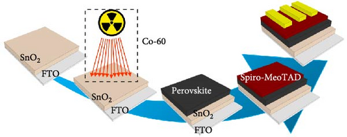
FTO glass substrates (Pilkington, TEC-8) were etched by a diluted HCl solution and Zn powder and subsequently cleaned with hellmanex, ethanol, acetone, and deionized H2O in an ultrasonic bath for 20 min. To form an amorphous SnO2 film, 0.1 M SnCl2·2H2O (Sigma-Aldrich) ethanol solution was prepared and was spin-coated at 3000 rpm onto FTO substrates for 30 s. The coated films are annealed in air at 185°C for 3 h [10]. Then, the amorphous SnO2 surface was treated by the gamma-irradiation source (CS06010-15042101 2/13/15, 0.370 Mbq, International Isotpor Inc.) for various gamma irradiation times. The used gamma-irradiation source was chosen to Co-60 emitting high energies gamma-rays such as 1.17 and 1.33 MeV to guarantee the formation of oxygen vacancies. Where gamma-irradiation source to sample distance was about 1 cm, and the effective area irradiated from gamma-rays was 1.5 × 1.5 cm2, as shown in the diagram of Figure 1.
2.2. Synthesis of PSCs
To synthesize MAPbI3 perovskite, the 50 wt.% of MAPbI3 precursor solution was made where both methylammonium iodide (MAI; GreatCellSolar) and lead (II) iodide (PbI2; TCI) were dissolved in 0.635 mL of dimethylformamide (DMF, Sigma-Aldrich). To form the corresponding adducts, 70 µL of dimethyl sulfoxide (DMSO, Sigma-Aldrich) was mixed into this solution [10]. The completely dissolved MAPbI3 solution was dripped onto the FTO/SnO2 ESL substrates and spin-coated for 25 s at 4000 rpm. During the spin-coating stage, 0.5 mL of diethyl ether (Sigma-Aldrich) was dripped onto the substrate for 15 s before the spin-coated was finished. Then, the coated film was annealed in two steps at 65°C for 1 min and at 100°C for 2 min. In addition, the CsFAMAPbIBr perovskite absorber layer was synthesized in ambient air by a two-step spin-coating process on the prepared substrates. First, the 0.6 g of PbI2 (TCI), 0.05 g of CsI (Sigma-Aldrich) in the mixed solvent of 0.95 mL DMF and 0.05 mL DMSO (Sigma-Aldrich) was coated on the SnO2 layer by the dynamic spin coating method at 3000 rpm for 30 s. The film was annealed at 70°C for 1 min. Second, the 7.2 mg of MABr (Greatsolar), 7.2 mg of MACl (Greatsolar), and 57.6 mg of FAI (Greatsolar) in the 1 mL of isopropanol (IPA, Sigma-Aldrich) was dropped on the as-coated PbI2 substrates during spin coating at 5000 rpm for 30 s, followed by annealing in an ambient condition at 150°C for 10 min. Thereafter, Spiro-MeOTAD, acting as HSL, was coated on perovskite films at 4000 rpm for 30 s. The HSL precursor solution was prepared by dissolving 80 mg spiro-MeOTAD, 28.5 µL of 4-tert-butyl pyridine, 17.5 µL of Li-TFSI (Sigma-Aldrich) solution (520 mg of Li-TFSI in 1 mL of acetonitrile) in 1 mL of chlorobenzene (Sigma-Aldrich). Finally, the Au electrode (80 nm) was evaporated by using a thermal evaporation system under a vacuum of 10−6 Torr.
2.3. Characterization
The morphology of the films, incorporating FTO/A-SnO2 or R-SnO2/perovskite structures, was examined by scanning electron microscopy (SEM, FlexSEM1000, Hitachi) at a resolution of 15 kV. Using field-emission SEM (FE-SEM, SU8010, Hitachi) at a resolution of 5 kV, the cross-sectional structures of the devices were observed. Current density–voltage (J–V) curves were measured under AM 1.5 one sun illumination condition using a solar simulator (Polaronix K201, McScience, Korea) and a Keithely 2401 source meter. The light intensity was adjusted by a KIER-calibrated Si reference cell having a KG5-filter. All the measurements were conducted by covering the devices with a metal mask with an effective active area of 0.09 cm2. The contact angle (phoenix 300touch) was analyzed by dispensing the perovskite precursor solution on the SnO2 substrate. The external quantum efficiencies (EQEs) were measured by the incident photon-to-current conversion efficiency system (IPCE, HS Tech, Korea) in the air. Electrochemical impedance spectroscopy (EIS) was performed using a potentiostat (SP-240, Biologic) under dark conditions from 0.5 to 1 V bias with the applied bias step of 0.1 V at frequency 10 Hz−1 MHz. X-ray photoelectron spectroscopy (XPS) was conducted with a ThermoScientific K-Alpha X-ray Photoelectron Spectrometer using monochromatized Al Kα under ultra-high vacuum conditions. To measure the valance band and the Fermi level of the ESLs, ultraviolet photoelectron spectroscopy (UPS, KBSI) equipped with a Kratos Axis ultra-delay line detector was performed.
2.4. Theoretical Calculations Based on the Density Functional Theory (DFT)
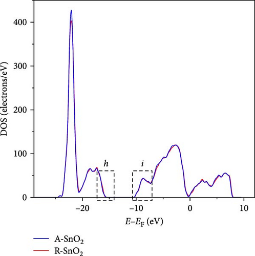
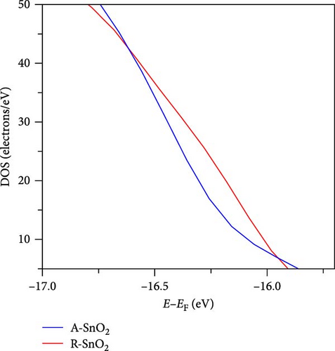
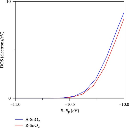
The DFT calculations were performed on the bulk phases of SnO2 to analyze the effect of gamma-ray irradiation. In DFT calculations, the Quantum Espresso package [16, 17] was utilized with the Perdew–Burke–Ernzerhof generalized gradient approximation function. In addition, ultrasoft pseudopotential is used to describe the core electrons of each atom, and an energy cutoff was set at 680 eV to predict the electronic structures. To optimize the atomic geometry, all atoms were fully relaxed until the force applied to them was less than 0.01 eV/Å. The crystal structure of SnO2 was modeled based on a previous experimental report [18], where the amorphous SnO2 structure was formed by ab initio molecular dynamics simulation procedure. In this modeling, the NVT ensemble for 0.24 ps with a time step of 0.5 fs was used, and the temperature was set to 3000 K, which is higher than the melting point of SnO2 [19]. For the integration of Newton’s equation of motion, the Verlet scheme was applied. To investigate the electronic structure, the density of states analysis was used. The optimized crystal structure of SnO2 exhibited lattice parameters of a = 0.4858 nm and c = 0.3208 nm, which showed a deviation of less than 0.012 nm when compared to previous studies [20]. Additionally, the bandgap of the crystalline SnO2 was 0.7 eV, differing by ~0.07 eV from prior research [21]. These comparisons validate the reasonable structure of the SnO2 used in this study. Subsequently, a 3 × 3 × 3 supercell of the optimized crystalline SnO2 was constructed to create amorphous SnO2.
3. Results and Discussion
Figure 1 schematically illustrates a procedure for the fabrication process of PSCs in an ambient atmosphere via low-dose gamma-irradiation treatment on an amorphous SnO2 surface. The Co-60 (10 μ Ci) irradiation source was used to irradiate amorphous SnO2 film with varying treatment times. To investigate the quantitative number of gamma-rays emitted from coin-type radiation sources depending on the irradiation times, we calculated this by considering the half-life of Co-60. The total emitted gamma-rays for 24, 72, and 168 h of irradiation times were calculated to be 1.432 × 10¹⁰, 4.296 × 10¹⁰, and 10.024 × 10¹⁰ Bq, respectively. The detailed number of irradiation gamma-rays is presented in Table 1. Hereafter, two amorphous SnO2 films with or without gamma-irradiation treatment are denoted as R-SnO2 or A-SnO2, respectively.
| Source activity | Effective source activity (Bq) | Irradiation treatment time (h) | Total emitted gamma-rays | |
|---|---|---|---|---|
| (μCi) | (Bq) | |||
| 10 | 3.7 × 10⁵ | 1.65743 × 10⁵ | 24 | 1.432 × 10¹⁰ |
| 72 | 4.296 × 10¹⁰ | |||
| 168 | 10.024 × 10¹⁰ | |||
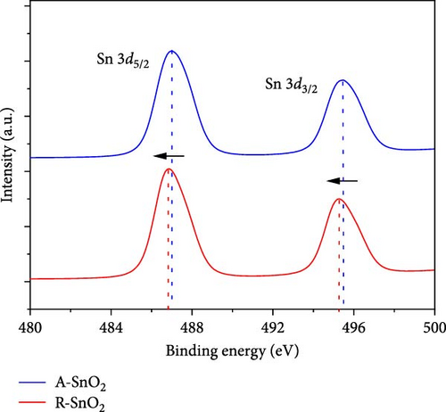
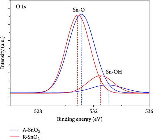
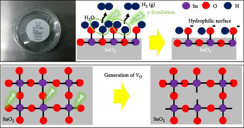
To ascertain the effect of gamma-irradiation on the amorphous SnO2 film, we investigated the XPS measurements of R-SnO2 and A-SnO2 films that were deposited on the FTO substrates. In this study, all processes were performed in an ambient air atmosphere with a relative humidity (RH) of 40%. Thus, in the presence of moisture, water (H2O) molecules can be adsorbed by either chemisorption or physisorption onto the SnO2 surface. According to McGrady et al. [14], H2O molecules attached to the surface of metal oxides were decomposed by gamma-irradiation to generate ─OH on the metal oxide surface. Although the activity of the adopted gamma-source in this study is relatively low (Table 1), the total gamma-rays irradiated for a long time are sufficient to affect the chemical bonding of the SnO2 layers. From XPS spectra (Figure 2a,b), two significant changes were observed. First, the Sn 3d spectrum of the A-SnO2 film (Figure 2a) depicts the binding energy (BE) of two peaks (Sn 3d5/2 and 3d3/2) at 487.01 and 495.46 eV, respectively [22], whereas the Sn 3d spectrum of the R-SnO2 film indicated that the BE peaks of Sn 3d5/2 and 3d3/2 were slightly shifted to ~486.85 and 495.28 eV, respectively. Second, the O 1 s state of A-SnO2 films was divided into two peaks at 531.14 and 532.9 eV, and the O 1 s state of R-SnO2 films was also divided into two at 530.8 and 532.4 eV. These peaks correspond to the BEs of the Sn─O and Sn─OH bonds, respectively (Figure 2b) [23]. Although the deconvolution was observed to be similar, the Sn─OH BE peak intensity of the R-SnO2 films was substantially increased compared to that of the A-SnO2 film. In summary, from the XPS spectra (Figure 2a,b), it was observed that the BE peaks of R-SnO2 film shifted to a lower BE and the BE intensity of the Sn─OH bond increased, all of which were caused by the gamma-irradiation in the presence of moisture. The increase of the ─OH peak intensity indicates the increase of the ─OH concentration in R-SnO2 films. Under gamma-irradiation, the radioactive energy decomposes H2O molecules adsorbed at the surfaces of SnO2 into H2 (g) and ─OH. Therefore, ─OH remains on the R-SnO2 surface, which makes the surface hydrophilic. An additional effect of continuous gamma-irradiation is the formation of oxygen vacancy (VO) [24]. The formation of VO during the annealing process is due to the continuous gamma-irradiation that breaks the Sn─O bonds by high energy and/or heat-induced from gamma-irradiation. In this study, the low BE shift of Sn 3d5/2 and 3d3/2 could be ascribed to change electron density of the Sn orbital, which is due to the difference electronegativity of Sn2+ (1.34) and Sn4+ (1.73) [25]. It means that the oxygen vacancy in R-SnO2 compensated through Sn4+ to Sn2+, leading to Sn4+─O─Sn4+ replacement Sn4+─O─Sn2+ bonds [26]. Combining the XPS results, we present the proposed mechanism of ─OH and VO formation by continuous gamma radiation on the surface of R-SnO2 in Figure 2c.
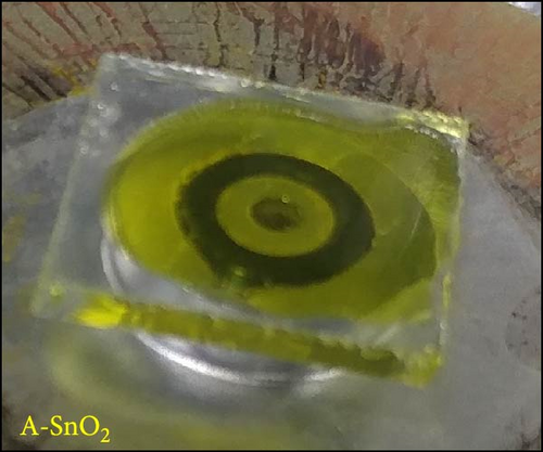
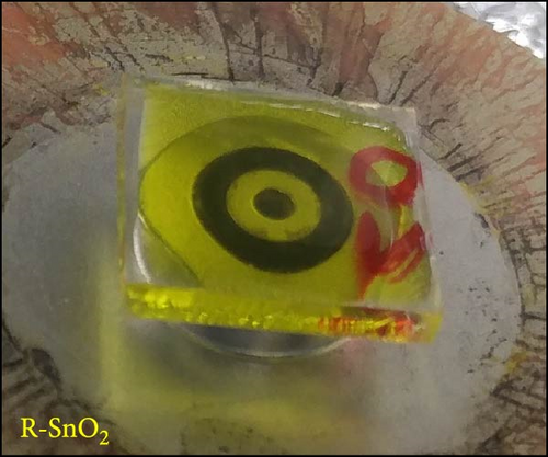
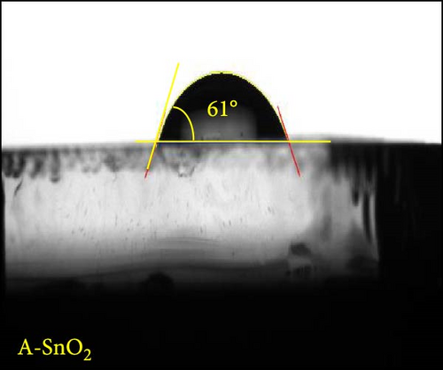
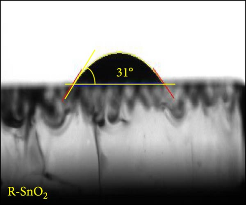
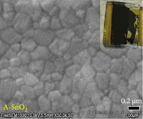
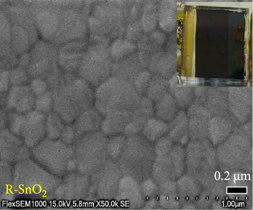
Digital camera images of perovskite solution dripped on different ESLs (Figure 3a,b) show that the perovskite solution on the R-SnO2 surface spreads better than the A-SnO2 surface. To explain this phenomenon, we measured the contact angle using perovskite solutions, as depicted in Figure 3c,d. Compared to the contact angle (61°) for the A-SnO2 surface, the R-SnO2 surface indicated a lower contact angle (31°). According to the nucleation theory, ESL surface properties, such as hydrophilicity and hydrophobicity, greatly influence the morphologies and properties of perovskite films [27, 28]. Assuming that the perovskite surface becomes super-hydrophobic, the thermal annealing of these surfaces can leave multiple pinholes due to the coarse grains not packed tight enough to interconnect with each other. Conversely, when the surface film becomes more hydrophilic, the uniformity of the film increases, but the nuclei density increases and grows to a small grain size. Therefore, it is necessary to properly control and closely monitor the surface properties between hydrophobicity and hydrophilicity to obtain a uniform grain size and simultaneously promote heterogeneous nucleation [13]. In this study, gamma-irradiation treatment on the surface of SnO2 films induced moderate hydrophilicity due to the ─OH generated at the surface and promoted the formation of uniform grains. To validate the evolution of perovskite grain according to the surface properties, we analyzed the surface SEM images. The surface SEM images of perovskite layers with varying ESLs (Figure 3e,f) show that the perovskite grains of the R-SnO2 are larger than those of A-SnO2. In addition, the R-SnO2-based perovskite grain completely covered the ESL region, while the A-SnO2-based perovskite film provided incomplete coverage (inset of Figure 3e,f).
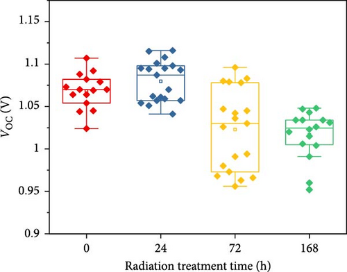
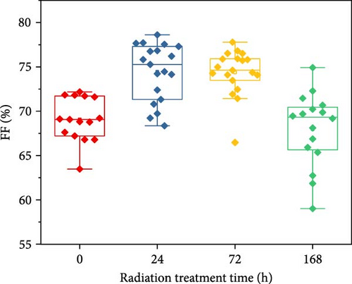
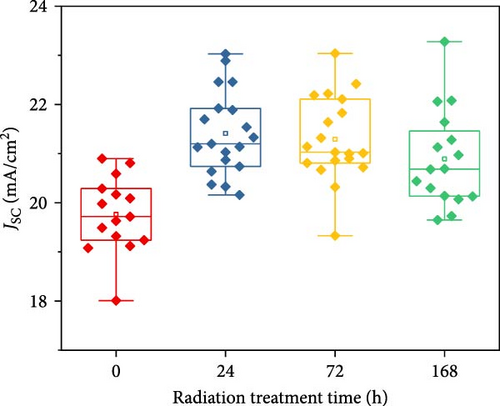
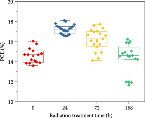
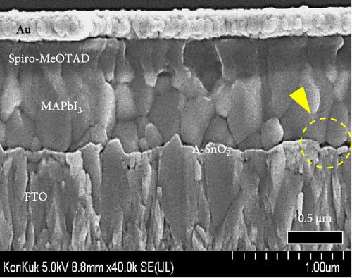
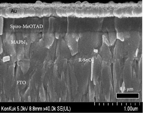
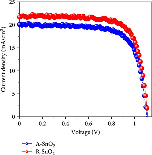
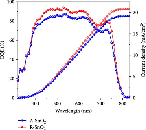
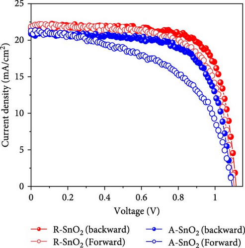
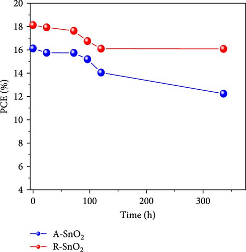
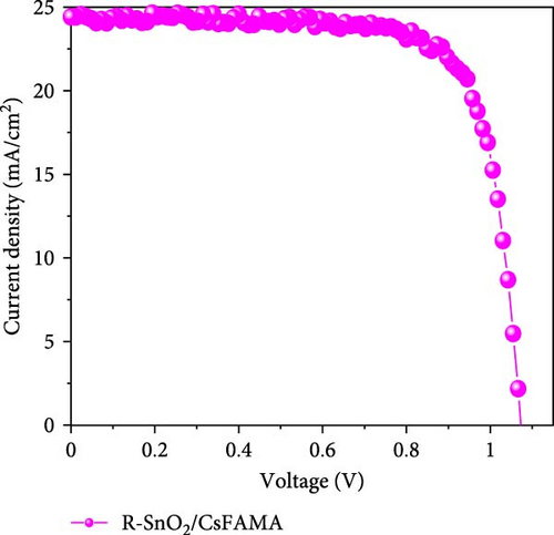
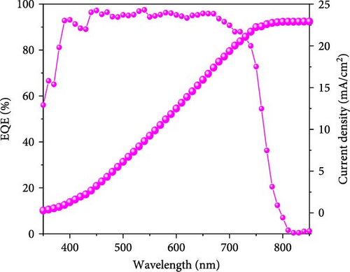
To demonstrate the gamma-irradiation effect, PHJ solar cells with the device architecture of FTO/ESL (A-SnO2 or R-SnO2)/MAPbI3/Spiro-MeOTAD/Au were synthesized. From Figure 4a–d, the optimal gamma-irradiation treatment time was determined to be 24 h considering the obtained PV parameters of more than 15 devices. The cross-sectional SEM images of the devices with varying ESLs (Figure 5a,b) show that the perovskite grains of the A-SnO2-based devices were relatively small and included some pinholes (indicated by yellow circles). In contrast, the R-SnO2-based device had larger perovskite grains with excellent uniformity. Figure 5c depicts one of the best J–V characteristics of the solar cells based on R-SnO2 and A-SnO2. The cell using A-SnO2 ESL exhibited a PCE of 16.05% with Jsc of 20.09 mA/cm2, Voc of 1.107 V, and fill factor (FF) of 72.18%. In contrast, the cell using R-SnO2 ESL substantially enhanced to 18.03% with an enhanced Jsc of 21.75 mA/cm2, Voc of 1.115 V, and FF of 74.35%. The EQE of the two devices was also investigated. From the EQE curves (Figure 5d), the Jsc values were calculated to be 21.00 mA/cm2 for R-SnO2 and 19.35 mA/cm2 for A-SnO2. Figure 5e depicts the hysteresis behavior of the solar cells based on two SnO2 ESLs. The R-SnO2-based solar cells exhibited a hysteresis index of 0.07, significantly lower than that (0.21) of the A-SnO2-based cell. The stability test of the unencapsulated solar cells was further investigated in an ambient environment with RH of ~40%, as shown in Figure 5f. The PCE of the A-SnO2-based cell rapidly dropped after 150 h, with a performance loss of >25% after 350 h. On the contrary, the PCE of the R-SnO2-based cell indicated outstanding long-term stability maintaining >90% of initial PCE up to 350 h in an air ambient condition. To further increase PCE, the MAPbI3 absorber was replaced by CsFAMAPbIBr synthesized under ambient-air. The obtained PV properties are indicated in Figure 5g. The CsFAMAPbIBr-based device using A-SnO2 ESL exhibited a PCE of 18.59% with a Jsc of 22.75 mA/cm2, Voc of 1.072 V, and FF of 76.28%. However, using R-SnO2 ESL, the PCE of the CsFAMAPbIBr solar cell was improved to 20.01% with a Jsc of 24.42 mA/cm2, Voc of 1.073 V, and FF of 76.37% (Figure 5g). In addition, EQE of CSFAMAPbIBr cell based on R-SnO2 ESL is shown in Figure 5h. From this curve, the Jsc value was calculated to be 23.04 mA/cm2.
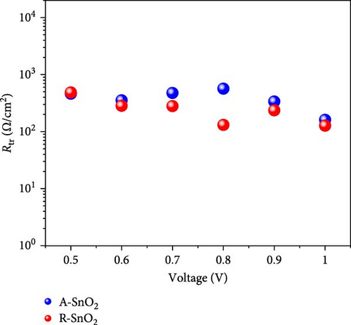
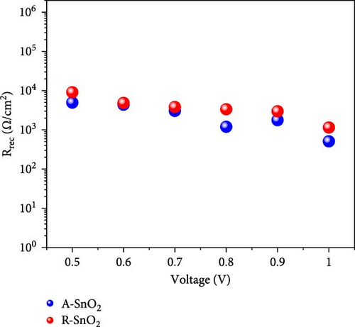
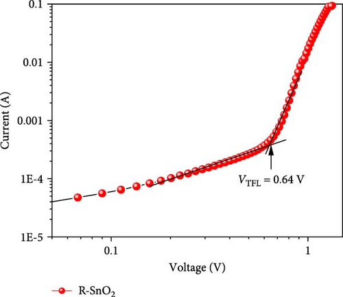
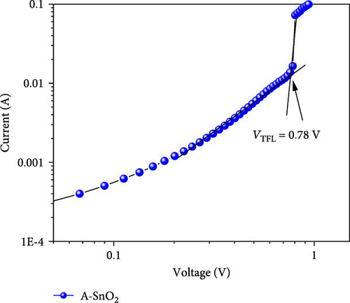
Using the EIS analyses, the charge transport dynamics were investigated [29]. Figure 6a indicates the Nyquist plots of A-SnO2- and R-SnO2-based cells measured under the applied voltage of 1 V in the dark. In the inset of Figure 6a, an equivalent circuit for fitting was shown. Typically, two arcs can be found in Nyquist plots: a first high-frequency arc is associated with charge transfer resistance (Rtr), and a second low-frequency arc is related with recombination resistance (Rrec) [30]. The measured smaller Rtr of the R-SnO2-based cell indicated faster charge extraction than that of the A-SnO2-based cell (Figure 6b). Moreover, the larger Rrec of the R-SnO2-based cell indicates less nonradiative charge recombination compared to the smaller Rrec of the A-SnO2-based device (Figure 6c). This is due to the few pinholes and the large MAPbI3 perovskite grain with less grain boundary, both acting as nonradiative charge recombination pathways. This result is in good agreement with the trap densities obtained from space charge limited current (SCLC), as shown in Figure 6d,e. From the measured VTFL values (0.65 and 0.78 V), the trap densities (Nt) of the two cells are calculated to be 8.4 × 10¹⁵ and 10.23 × 10¹⁵, respectively, using equation Nt = 2εε0VTRL/eL2, where ε is the dielectric constant of the perovskite layer, ε0 is the dielectric constant of vacuum, and L is the film thickness [31]. To further support the enhancement of the faster charge extraction, we evaluated the conductivity using the dark I–V curves (Figure 6f). The conductivities of the R-SnO2 and A-SnO2 ESLs were evaluated using , where A is the active area, σ is the direct current conductivity, d is the thickness of each ESL, and R is the resistance. The σ values of R-SnO2 and A-SnO2 ESLs were calculated to be 3.34 × 10⁻³mS/cm and 2.95 × 10⁻³mS/cm, respectively, which demonstrated that the gamma-irradiation improved carrier transport. In general, the existence of Vo in SnO2 leads to enhanced charge transport and affected the conductivity by reduced resistivity [32, 33].


As depicted in the EIS and J–V results, gamma-irradiation demonstrated lower nonradiative recombination and faster charge extraction, leading to enhanced PCEs of PSCs.
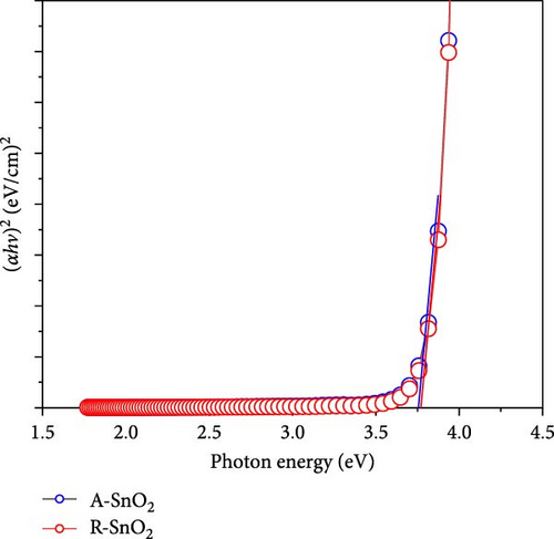
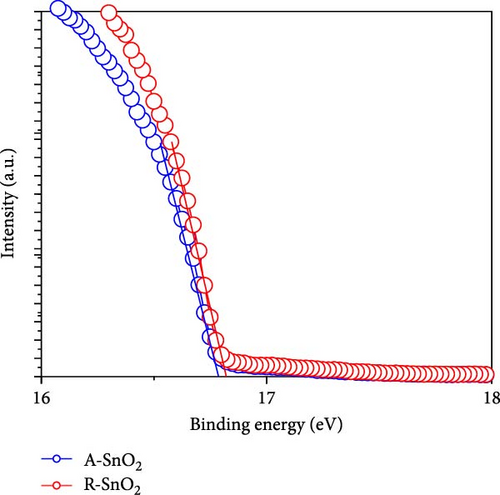
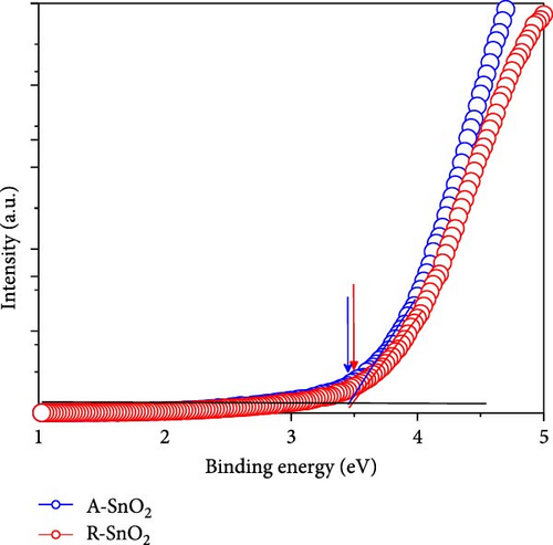
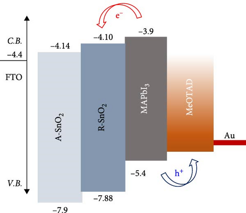
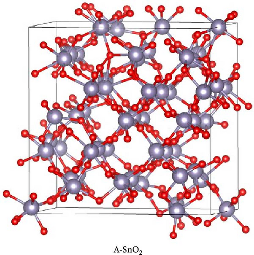
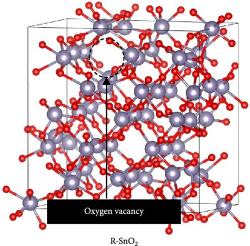
To gain more insight into the radiation effect on amorphous SnO2, the UPS and UV–visible spectroscopy were performed to get the detailed band-offset. From the Tauc plot (Figure 7a), the bandgaps of the R-SnO2 and A-SnO2 ESLs were obtained to be 3.78 and 3.75 eV, respectively. To complete the band-offset, the secondary electron cutoff energy (Ecutoff) and Fermi-level (EF) of the R-SnO2 and A-SnO2 films were obtained from the UPS spectra shown in Figure 7b,c. Based on these results, the EF of R-SnO2 and A-SnO2 films were determined to be 4.40 and 4.44 eV, and their valence band maximums (VBMs) of R-SnO2 and A-SnO2 were calculated to be 7.88 and 7.9 eV, respectively. In addition, the conduction band minimums (ECBM) of R-SnO2 and A-SnO2 were calculated to be 4.10 and 4.14 eV, respectively. Combining these data, the complete band-offset of the full cells is illustrated as shown in Figure 7d. Interestingly, the EF of R-SnO2 moved upward than that of A-SnO2 because the generation of Vo in SnO2 can produce a shallow donor level, inducing the n-type property of SnO2 [34, 35].To further prove the observed oxygen vacancy effect in R-SnO2, DFT calculations were performed, as shown in Figure 7e,f. The structures of both R-SnO2 and A-SnO2 were shown where the removal of oxygen atom in R-SnO2 by radiation treatment is indicated by black dotted circle. The interesting result of the oxygen vacancy formation of R-SnO2 obtained by the DFT calculation is well matched the band diagram (Figure 7g–i). These DFT and band-offset calculation results clearly suggest that the formation of Vo in R-SnO2 led to more n-type property than pristine SnO2. Therefore, the effect of V0 can induce to enhance the electron density, following the n-type property of R-SnO2.
4. Conclusions
To summarize, herein, we have reported the influence of gamma-irradiation treatment on the amorphous SnO2 ESLs and its impact on the PV performance of planar PSCs. It was observed that the gamma-irradiation substantially modified the properties of amorphous SnO2 ESLs. First, low-dose gamma-irradiation induced the formation of ─OH ions on the SnO2 surface, making the surface hydrophilic, owing to the decomposition of chemisorbed/physisorbed H2O vapor in amorphous ESL. Second, the hydrophilic surface enhanced the crystal growth kinetics, thereby increasing the perovskite grain size. Third, gamma-irradiation enhanced the ESL conductivity via the generation of oxygen vacancies. Through these synergistic effects of gamma-irradiation treatment on the amorphous SnO2 film, a champion efficiency of 18.03% of MAPbI3 film-based device was achieved, which was higher than that (16.05%) of a pristine device. In addition, a maximum PCE of 20.01% was achieved using gamma-irradiated SnO2-based CsFAMAPbIBr PHJ solar cells presenting the potential as a new surface treatment technique.
Conflicts of Interest
The authors declare no conflicts of interest.
Author Contributions
Beomjun Park and Kyungeun Jung contributed equally to this work.
Funding
This research was supported by Challengeable Future Defense Technology Research and Development Program through the Agency for Defense Development (ADD), funded by the Defense Acquisition Program Administration (DAPA) in 2024 (Nos. 912765601 and UI247016TE). This work was also supported in part by the Human Resources Development Program of the Korea Institute of Energy Technology Evaluation and Planning (KETEP) grant funded by the Ministry of Trade, Industry and Energy, Republic of Korea (No. RS-2023-00237035).
Acknowledgments
This research was supported by the Challengeable Future Defense Technology Research and Development Program through the Agency for Defense Development (ADD), funded by the Defense Acquisition Program Administration (DAPA) in 2024 (No. 912765601 and UI247016TE). This work was also supported in part by the Human Resources Development Program of the Korea Institute of Energy Technology Evaluation and Planning (KETEP) grant funded by the Ministry of Trade, Industry and Energy, Republic of Korea (No. RS-2023-00237035).
Open Research
Data Availability Statement
The data that support the findings of this study are available from the corresponding author upon reasonable request.


