Graphene-Modified Photoelectrode for Efficient and Cost-Effective Dye-Sensitized Solar Cells
Abstract
Dye-sensitized solar cells (DSSCs) have been attracted as a real class of building-integrated photovoltaic (BIPV) owing to its natural controllable color transparency, working ability in diffuse light, and low-cost fabrication. The low photoconversion efficiency (PCE) is the main obstacle for BIPV market. The bilayered structure based on mesoporous TiO2 nanoparticles (NPs) along with TiO2 blocking layer was introduced to obtain high PCE by optimizing the dye adsorption, avoid recombination via direct electrolyte contact, and enhance light-harvesting ability by providing scattering centers. However, the bilayered structure based on mesoporous TiO2 network offers inferior charge transfer, thus higher recombination and, consequently, low PCE. In our previous studies, we have developed graphene/TiO2 blocking layer, graphene/TiO2 transparent layer, and scattering layer and analyzed individually to improve the electron transport and reduce recombination. In the current work, we have demonstrated the integrated optimized photoelectrode-based DSSCs via the above-mentioned previously developed photoelectrode components with Pt and graphene/polyaniline (PANI) cost-effective counter electrode. Optical property analysis and electrochemical impedance spectroscopy (EIS) have shown that graphene-modified optimum components of photoelectrode have effectively improved the electron transport and light-harvesting ability. Electron lifetime, diffusion coefficient, and diffusion length have been increased by ~87%, ~20%, and ~11%, respectively, as compared to control DSSC based on commercial paste. Consequently, 5.94% of PCE was achieved, which is 20% higher than the DSSCs fabricated with commercial pastes. Moreover, DSSCs based on optimized photoelectrode with graphene/PANI counter electrode have shown 4.04% PCE, which is ~70% of the PCE that was achieved with Pt.
1. Introduction
Global energy consumption is increasing at an alarming rate. According to the International Energy Agency (IEA) 2024 report, global electricity demand is expected to increase by 3.4% annually through 2026 [1]. Higher energy demands are also causing higher CO2 emissions, since coal is still the largest source of electricity in the world [2]. Recently, the concept of zero energy building based on building-integrated photovoltaic (BIPV) has been introduced to meet the higher energy challenges and reduce greenhouse gas emissions [3].
BIPV system-based windows can perform multiple functions such as building exterior finishing, curtain wall, green houses for plants and power generation [3, 4]. Dye-sensitized solar cells (DSSCs) have been developed as a true class of BIPV owing to its intrinsic controllable color transparency which is appropriate for the construction of light openings [5–7]. The controllable natural color transparency of DSSC originated from the dye-anchored mesoporous TiO2. Customized color windows can be developed with the integration of different morphologies or particle size of TiO2 and different types of dyes [8, 9]. DSSC performs better in cloudy or ambient light as compared to other solar technology. Moreover, it is quite cost-effective and offers simple roll-to-roll manufacturing processes [10–12].
DSSC is comprised of three components: photoelectrode or working electrode, electrolyte, and counter electrode. Working or photoelectrode is composed of mesoporous semiconducting TiO2 film sensitized with dye [13, 14]. The counter electrode is typically composed of electrocatalytic platinum film [15]. The active medium of both electrodes is supported by conducting substrate. Moreover, electrolytes are sandwiched between both photo and counter electrodes. DSSC working principle is mimic with photosynthesis; typically, light enters from the photoelectrode through the transparent conducting substrate where dye molecules absorb photons and get excited. The excited dye molecules inject electrons into the conduction band (CB) of mesoporous semiconductors, which then percolate across the TiO2 framework and reach to the counter electrode by external connection or load, and then tri-iodide ions pick up the electrons at the electrocatalytic surface of counter electrode and convert into iodide ion. Finally, these iodide ions of the electrolyte restore the dye to its initial state. The difference in the potential of TiO2 fermi level and electrolyte reduction potential gives up open circuit potential of DSSC [14].
The low photoconversion efficiency (PCE) of DSSC is the main challenge for the success of BIPV market [6]. Several factors are responsible for its low PCE, for instance, electron recombination, sluggish electron transfer, and low light-harvesting ability [16, 17]. Mesoporous TiO2 offers a balance between a large surface area for dye attachment and appropriate pore size for both electrolyte and dye molecule diffusion [14, 18, 19]. Moreover, simple TiO2 nanoparticle (NP) network also transmits appreciable light to the dye. However, the porous structure of TiO2 develops inconsistent and rough interface with fluorine-doped tin oxide (FTO) glass surface which results in undesirable leaking of electrolyte to the FTO which causes direct electron recombination by electrolyte [20]. Furthermore, mesoporous TiO2 permits slow electron transport due to random paths for diffusion, which causes higher electron recombination and, therefore, loss of PCE. The optical transmittance of mesoporous TiO2 is excellent for capturing a large number of photons for the dye; however, it transmits a high proportion of light without harvesting [21]. Several researchers have proposed different morphologies of TiO2 based on large sized particles to avoid this loss [22–26]. Blending of larger particles with small sized, hierarchical structures, core–shell structures, and many more morphologies have been developed to scatter the light effectively without sacrificing dye loading capability due to low surface area of large particles [27–31]. Nevertheless, scattering structures just like transparent TiO2 films are unable to transport electrons at a fast rate.
The above-mentioned issues of photoelectrode have been partially addressed through establishing the bilayered structure by Gratzel and coworkers. They have grown a TiO2 blocking layer on conducting glass via TiCl4 treatment subsequently formed two layered structure that is TiO2 transparent layer at the base while scattering layer at the top. They achieved a significantly higher PCE of 11% with 0.16 cm2 active area [32]. This pioneered work of Gratzel group demonstrated that for an efficient DSSC, there should be three components of photoelectrode: blocking layer, transparent, and scattering layer. Since blocking layer is indeed very thin and apparently just a modification of FTO, therefore, overall structure can be called TiCl4-treated bilayered photoelectrode. Later, several researchers reported different structures and composites for optimizing the properties of bilayered photoelectrode with or without blocking layer [33–35]. For instance, Dissanayake, Senthuran, and Senadeera [22] reported double-layered photoelectrode, mesoporous transparent layer based on P25, and scattering layer based on hierarchically structured submicron size particles. The authors have claimed ~10% higher PCE as compared to the device without scattering layer. Most of the reports have been focused on enhancing scattering effects to improve light-harvesting capability without sacrificing dye loading amount. However, electron transport performance, which is another important factor of photoelectrode for an effective and successful transfer of photogenerated electron, specifically in the double-layered integrated form, has been ignored.
In the above context, in our previous work, we modified FTO glass and TiO2 interface via graphene/TiO2 compact layer to impede recombination reaction, graphene-incorporated TiO2 multiphase transparent layer to enhance electron transport efficiency/reduce recombination, and graphene-loaded submicron sphere scattering layer photoelectrode for DSSCs individually [36–38]. In all the mentioned studies, high-quality graphene has been synthesized by solvent exfoliation method incorporated in TiO2 which has shown drastic improvement in electron transport parameters, which in turn improve PCE. Graphene is well-known for its exceptional electrical mobility and mechanical properties [39]. Mostly, graphene has been used in the form of graphene oxide (GO) or reduced graphene oxide (rGO) due to high yield and ease of dispersion [36]. However, rGO after complete reduction cannot restore intrinsic graphene properties completely; due to this reason, we have employed solvent-exfoliated graphene which offers original properties of graphene and optimized each component of photoelectrode separately. Moreover, previously, we have also developed cost-effective counter electrode based on graphene/polyaniline (PANI) [40]. Graphene/PANI-based counter electrode has shown comparable electrocatalytic performance with Pt, while their cost is negligible. Defective structure of graphene has benefit that it provides a higher population of active sites for catalytic reaction but low electron transport. On the other hand, solvent-exfoliated graphene provides better conductivity but low active sites. PANI in the emeraldine salt form is a conjugated polymer which offers excellent conductivity and electrocatalytic activity. Graphene and PANI combination can provide synergistic effects of electron transport with enhanced electrocatalytic performance [40, 41].
Therefore, in the current work, we have demonstrated DSSC based on optimized photoelectrode, fabricated by the integration of our previously developed graphene/TiO2 blocking layer, transparent layer, and scattering layer with Pt and cost-effective graphene/PANI counter electrodes. The active area for fabrication has been opted 1 cm2 relatively large to explore the true potential for commercialization.
2. Materials and Methods
2.1. Materials
FTO conducting glass, TiO2 nanopowder (≤21 nm, anatase, Sigma Aldrich), titanium isopropoxide (TTIP) (97%≥, Sigma Aldrich), graphite flakes (+mesh ≥75% min, Sigma), absolute ethanol (99.98%, AnalaR), ethyl cellulose (Sigma Aldrich), acetonitrile (99.9%≤, Merck), ammonia aqueous solution (25%, Merck), glacial acetic acid (Merck), deionized water (DI), hydrochloric acid (37%, Merck), aniline (98%≥, R&M Chemicals, UK), ammonium persulphate (≤98%, Sigma), electrolyte (HP, I−/I3−), N719 dye, sealant surlyn, 18-NRT TiO2, and Pt paste were purchased from Greatcell Solar Materials the former Dyesol, Australia.
2.2. Fabrication of Graphene/TiO2 Blocking Layer
Graphene dispersion and paste were synthesized as reported in our previous work [36]. FTO glass was cleaned with ethanol and DI water and then passed through the continuous furnace at 500°C to remove any possible contaminants. Graphene paste was tape cast on cleaned glass followed by drying at 80°C in air; this step was repeated twice to get the required graphene density on FTO surface. After drying, graphene-coated FTO was sintered in a furnace at 500°C in air. For the preparation of TiO2 sol–gel, 0.1 M solution of TTIP was prepared in absolute ethanol. Before adding TTIP, 0.1 mL of HCl (conc) was added in 100 mL of solution. After getting a clear solution, the prepared sol–gel was left to age for 1 day. Later, the prepared sol–gel was spin-coated on graphene-coated FTO at 1200 rpm for 15 s, followed by drying at 60°C on hotplate in air. After three times coating and drying, the sample was sintered in a furnace as done before for graphene coating.
2.3. Fabrication of Graphene-Incorporated TiO2 Transparent Layer
Graphene-incorporated transparent paste was prepared as reported in our previous work; for detailed TiO2 NPs and paste preparation method, refer to Shahid et al. [37]. Typically, graphene dispersion was added during preparation of TiO2 paste so that it became 0.0025 wt.%. This graphene/TiO2 paste was printed on pre-prepared FTO coated with graphene/TiO2 blocking layer using 48T screen. After screen printing films were left in airtight box to remove trap air from the film, it was later dried in the continuous furnace at 80°C. The printing and screen and drying processes were repeated thrice to get appropriate film thickness and then sintered in continuous furnace gradually at 510°C in air.
2.4. Fabrication of Graphene/TiO2 Submicron Sphere Scattering Layer
Submicron sphere scattering particles were prepared and blended with NPs as reported [38, 42]. Submicron spheres were blended with 20 wt.% TiO2 NPs to get optimum surface area or pore size and improve interconnectivity between particles. During paste preparation, graphene dispersion was added to make its concentration in the paste 0.01 wt.%, as optimized in our previous study [38]. This scattering paste was screen printed one time on graphene/TiO2 transparent paste-coated FTO, subsequently drying and sintering at 80°C and 510°C in air, respectively. Before drying, samples were kept in an airtight box as done in previous step to remove air bubbles.
2.5. Fabrication of Pt and Graphene/PANI Counter Electrodes Assembling of DSSC
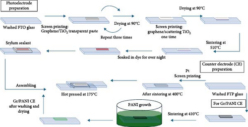
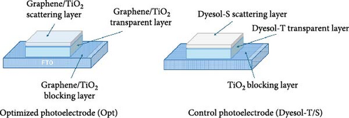
Graphene/PANI and Pt counter electrodes were prepared as reported in our previous work [40] and demonstrated in Figure 1a. DSSCs were assembled according to the established method. Typically, firstly, fabricated photoelectrodes were soaked in N719 dye solution for overnight. Holes for electrolyte filling on FTO glass were made by programmable sand blasting machine before deposition of active film. Photo and counter electrodes were assembled by thermoplastic sealant via hot press at 170°C. Electrolyte was filled using vacuum desiccator through prepared holes. Finally, the holes were covered with aluminum foil, and contacts were made using ultrasonic soldering machine. For comparison, reference DSSCs were fabricated using commercial Dyesol-T and Dyesol-S pasts following the same procedure of fabrication as mentioned above. TiO2 compact film was also formed on FTO surface without graphene for reference DSSCs. Configuration of fabricated photoelectrodes that are optimized and control (Dyesol-T/S) are shown in Figure 1b. The devices fabricated based on these photoelectrodes are denoted as Opt-Pt for optimized photoelectrode with Pt counter electrode, Opt-Gr/PANI optimized photoelectrode with Gr/PANI counter electrode, and control DSSCs as Dyesol-T/S.
3. Characterization and Testing
Field emission scanning electron microscope (FESEM) (Carl Zeiss AG, Supra 55VP) was used to study the morphology of optimized photoelectrode. Energy-dispersive X-ray spectroscopy (EDX) built in with FESEM setup was used to acquire elemental color mapping. A UV-Vis diffuse reflectance spectrophotometer (Agilent Technologies, Cary Series) has been employed to measure optical properties of photoelectrodes. Keithley 2420 digital source meter was used to measure J–V curves of fabricated devices under 100 mW/cm−2 (1.5 AM) illuminated condition. Incident photon to current conversion efficiency (IPCE) (Dyesol, model: S75ACW) was used to measure quantum efficiency of devices. EIS was conducted using Gamry Instruments from 100 to 100 KHz with the AC potential of 10 mV.
4. Results and Discussion
4.1. Morphology and Optical Property Analysis of the Optimized Photoelectrode
Figure 2a shows a FESEM image of optimized photoelectrode from the cross-section, composed of the graphene–TiO2 blocking layer, graphene/TiO2 transparent layer, and graphene/TiO2 scattering layer. The labeling indicates a three-layered structure; however, the blocking layer cannot be clearly seen as it is too thin ~80 nm as reported in our previous work [36]. The interfacing of the layers is compact; there is no evidence of cracking. The scattering layer is composed of submicron spheres and NP blend. The transparent film is composed of NPs that are compact on the blocking layer and FTO surface. The overall film thickness is estimated as ~16 µm, while transparent film thickness is around ~12.5 µm.

Figure 2b shows the transparent layer from the top; NPs are distributed uniformly without appreciable aggregation that is why the film turned out to be transparent. How the graphene/TiO2 blocking layer looks like can be seen in our previous work [36]. It seems like a compact film. TiO2 covered the graphene-coated FTO thoroughly. Figure 2c depicts the cross-sectional image of Dyesol-T/S photoelectrode (Dyesol-T main transparent layer and Dyesol-S scattering layer) from the interface. Scattering particles are submicron size and seem large crystalline rather than aggregated multicrystalline. On the other hand, submicron spheres of optimized photoelectrode scattering layer are embedded with NPs having almost uniform shape with variable size ~200–450 nm. These scattering spheres are formed by the integration of aggregated small crystallites, thus providing better surface area for dye adsorption as compared to the large size crystals shown in Dyesol-S.
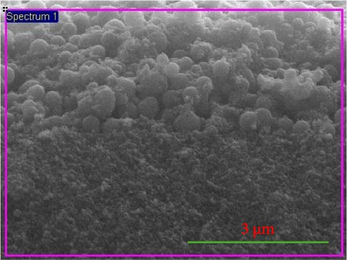
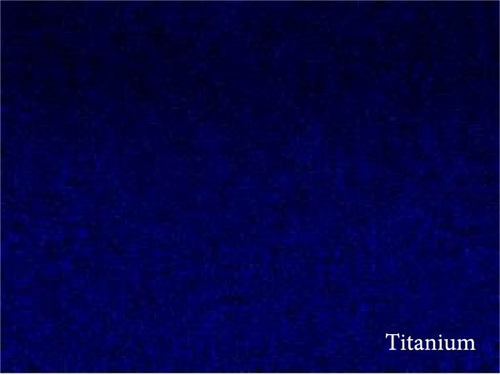
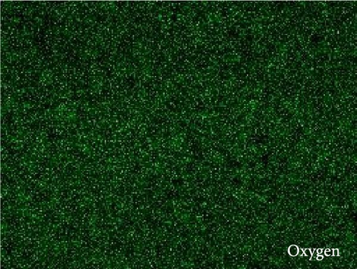
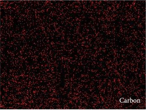
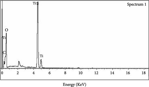
The EDX mapping was done from the interface of the transparent TiO2 and scattering layer shown in Figure 3a–e. Figure 3b–d shows the presence of mainly three elements in the film, titanium, oxygen, and carbon, which is attributed to the graphene/TiO2 composite film. Moreover, evenly distribution of carbon is ascribed to uniform graphene dispersion in TiO2 matrix.
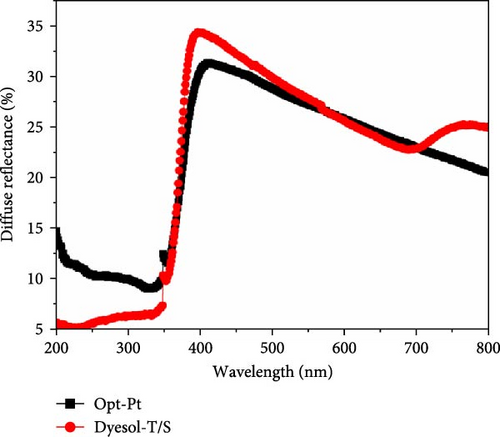
The light scattering capability of optimized and control photoelectrodes has been analyzed by acquiring diffuse reflectance spectra from 200 to 800 nm. Figure 4 shows the diffuse reflectance spectrum of Opt and Dyesol-T/S photoelectrodes. The measured diffuse reflectance of Opt photoelectrode is significantly higher in UV and nonvisible region than Dyesol-T/S that is probably due to the multiphase TiO2 of transparent layer. Around the beginning of visible region ~400 nm, the diffuse reflectance seems to be increased abruptly, where Dyesol-T/S which is the control photoelectrode leads till 550 nm. Afterward, the Opt photoelectrode has shown slightly better reflectance to 700 nm than the control photoelectrode; the better scattering ability in this region ~550–700 nm is beneficial for effective light harvesting using N719 dye. Dyesol-T/S has shown a little hump in the curve around 700 nm that is attributed to the aggregated large particles as seen in FESEM images. The results show that control photoelectrode has better capability of light scattering as compared to Opt before ~550 nm due to large size particles, while in desirable region, Opt performed relatively better. In our previous work, it has been demonstrated that the presence of graphene in scattering layer does not support the scattering effect [38]; rather, it slightly decreased the diffuse reflectance.
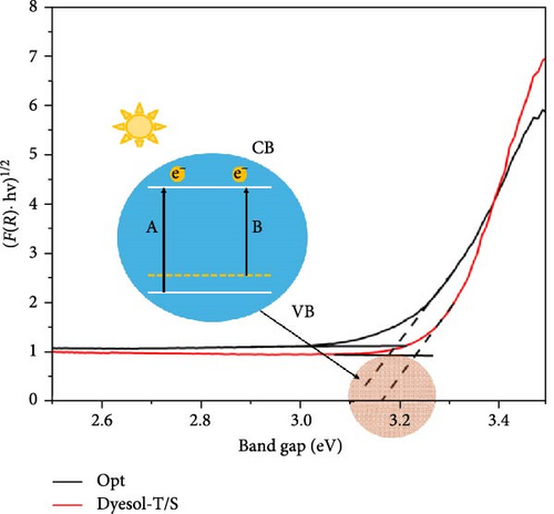
The band gap was calculated using diffuse reflectance data as shown in Figure 5. The optical absorption coefficient is red-shifted on comparison with Dyesol-T/S, showing the decrease in the band gap energy. The decrease in band gap energy of Opt is due to the presence of graphene. Figure 5 inset shows a schematic of band gap reduction; a little decrease in the band gap helps to create an impurity state between valence band (VB) and CB which can increase the number of photoelectrons and accelerate charge transfer consequently improving photovoltaic performance [43].
5. Photovoltaic Performance Evaluation of DSSC Based on the Optimized Photoelectrode
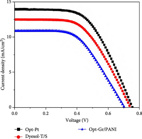
The photovoltaic performance of DSSCs was estimated using the J–V curve taken at one sun irradiation (Figure 6). The Table 1 shows the photovoltaic parameters of DSSCs based on; commercial paste photoelectrode (Dyesol-T/S),an optimized photoelectrode (with Pt and Gr/PANI counter electrode), as well as data from our previous work for comparison. The Dyesol-T/S showed 12.45 mA/cm2Jsc, 0.74 Voc, and 0.538 FF, resultantly, 4.96% PCE. The DSSC based on Opt-Pt photoelectrode has shown 13.68 mA/cm2JSC, 0.756 V Voc, and 0.57 FF values, consequently 5.94% PCE which is ~20% higher than control DSSC (Dyesol-T/S). Table 1 shows that all photovoltaic parameters are almost better than commercial paste-based DSSC. The Voc is somewhat the same for both DSSCs optimized and commercial based pastes; however, FF and JSC values of Opt-Pt photoelectrode DSSC are significantly higher than commercial-based DSSC, which are responsible for better PCE of Opt-Pt. The Opt-Gr/PANI-based DSSCs have shown relatively low photocurrent density of 10.834 mA/cm2; thus, PCE of 4.041% was obtained. Table 1 is extended with the photovoltaic parameters of our previous studies on DSSCs based on graphene/TiO2 blocking layer, transparent layer, and scattering layer for reference, since the presented work is the integrated design of photoelectrode based on all these layers. The presented parameters show that DSSCs with graphene/TiO2 blocking layer have shown 5.117% PCE which is significantly higher than Dyeol-T (without blocking layer) and relatively better than transparent and scattering layer-based DSSCs. The higher PCE of this graphene/TiO2 blocking layer-based DSSCs is mainly contributed by higher FF which is obtained due to better connectivity of TiO2 with substrate and lower recombination. These results imply that blocking layer is the most effective components of photoelectrode against recombination. Moreover, graphene/TiO2 transparent layer-based DSSCs have shown 4.825% PCE (without blocking layer) which is much better than commercial paste-based DSSC (Dyesol-T). Moreover, graphene/TiO2 scattering layer DSSCs displayed 4.959% PCE; for these devices, commercial Dyesol-T was used to fabricate transparent layer. Therefore, the overall integrated optimized photoelectrode has shown combined enhanced PCE due to the contribution of all previously optimized components. Table 2 shows the comparison of photovoltaic performance of the current work with some of the previous work based on bilayered photoelectrodes. It seems that the PCE of the current work is competitive in terms of the active area as it is established that PCE decreases with the increase in active area.
| Devices | FF | Voc (V) | Jsc (mA/cm2) | ɳ (%) |
|---|---|---|---|---|
| Dyesol-T/S | 0.538 | 0.74 | 12.452 | 4.96 |
| Opt-Pt | 0.574 | 0.756 | 13.68 | 5.944 |
| Opt-Gr/PANI | 0.527 | 0.708 | 10.834 | 4.041 |
| Dyesol-T [36]a | 0.492 | 0.685 | 10.148 | 3.423 |
| Gr/TiO2 blocking layer [36]a | 0.616 | 0.743 | 11.184 | 5.117 |
| Gr/TiO2 transparent layer [37]a | 0.553 | 0.718 | 12.145 | 4.825 |
| Gr/TiO2 scattering layer [38]a | 0.489 | 0.712 | 14.247 | 4.959 |
- Abbreviation: DSSCs, dye-sensitized solar cells.
- aPhotovoltaic performance presenting from our previous studies for comparison.
Photoelectrode (bilayered) |
FF | VOC (V) |
JSC (mA/cm2) |
PCE (%) |
Active area (cm2) |
Ref./year |
|---|---|---|---|---|---|---|
| Nb2O5–rGO/TiO2 | 0.58 | 0.72 | 14.70 | 6.4 | Not given | [44]/2024 |
| TiO2/CeO2 | 0.47 | 0.766 | 20.21 | 7.25 | 0.16 | [45]/2023 |
| 1% Cd–TiO2/TiO2 | 0.609 | 0.73 | 5.55 | 2.47 | Not given | [46]/2023 |
| Active carbon/TiO2+ SrTiO2 | 0.55 | 0.713 | 14.87 | 5.87 | Not given | [47]/2022 |
| TiO2 nanoparticles (NPs)/TiO2 hollow spheres | 0.59 | 0.69 | 12.02 | 5.01 | 0.25 | [31]/2022 |
| TiO2–graphene/TiO2 | 0.64 | 0.70 | 10.10 | 4.49 | 1 | [48]/2021 |
| TiO2 NPs/TiO2 nanowires | 0.56 | 0.78 | 22.67 | 9.90 | 0.16 | [49]/2019 |
| Opt-Pt | 0.574 | 0.756 | 13.68 | 5.944 | 1 | This work |
- Abbreviation: PCE, photoconversion efficiency.
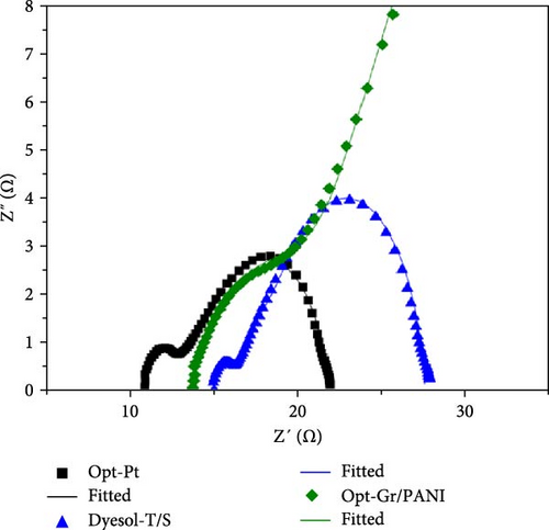
Electrochemical impedance spectroscopy (EIS) was done to evaluate the kinetics of electron transport and recombination in Opt-Pt, Opt-Gr/PANI, and Dyesol-T/S DSSCs in the dark at −0.78 V. The Nyquist plots are given in Figure 7, and the detailed fitted parameters are tabulated in Table 3. Nyquist plots are composed of two semicircles; the first semicircle represents a high-frequency region. Its diameter corresponds to the charge transfer resistance at counter electrode (RCT) and relevant double layer capacitance (Cdl). The horizontal distance from the origin to the semicircle beginning point is measure of sheet resistance (RS). The other semicircle represents the charge transfer kinetics of photoelectrode active layer and with electrolyte interface. The diameter of this second semicircle gives recombination resistance (RBR), and its imaginary component corresponds to the chemical capacitance (Cµ).
| Sample | RS (Ω) |
Rt (Ω) |
RBR (Ω) |
ωmax (Hz) |
τn (s) |
Dn (cm−2) |
ns (cm−3) |
Ln (µm) |
σn (s/cm2) |
|---|---|---|---|---|---|---|---|---|---|
| Optimized | 11 | 4.2 | 9.02 | 9.87 | 1.01 × 10⁻¹ | 5.42 × 10−05 | 3.71 × 10¹⁷ | 23.4 | 6 × 10−07 |
| Dyesol-T/S | 14.94 | 6.3 | 11 | 10.19 | 9.81 × 10⁻² | 4.5 × 10−05 | 2.9 × 10¹⁷ | 21.1 | 4 × 10−07 |
| Opt-Gr/PANI | 13.38 | 10.44 | 16.08 | 3.82 | 2.62E−01 | 1.5E−05 | 5.3 x× 1017 | 19.8 | 2 × 10−07 |
- Abbreviation: DSSCs, dye-sensitized solar cells.
The Bisquert transmission line model [44] was used for detailed analysis. Calculated or fitted parameters are given in Table 3. Opt-Pt DSSCs have shown relatively low RS as compared to Opt-Gr/PANI and Dyesol-T/S DSSCs, while Opt-Gr/PANI has little bit less RS which indicates appropriate conductivity of graphene and PANI electrocatalytic film. The less RS value of Opt-Pt DSSCs is owing to graphene and TiO2 compact film. Graphene improved the interconnectivity of the interface, and TiO2 compact thin film avoided any penetration of electrolyte. This combined effect of graphene/TiO2 blocking layer has reduced the RS. The second semicircle of Dyesol-T/S is comparatively large with Opt-Pt, and the straight line at the beginning of second semicircle is showing large Rt and RBR, while Opt-Gr/PANI has shown very high RBR and Rt; the exact fitted values are depicted in Table 3. It shows that Opt-Pt has the least Rt and RBR as compared to other DSSCs; Opt-Gr/PANI even has shown approximately threefolds higher Rt than Opt-Pt. Opt-Pt and Opt-Gr/PANI have the same type of photoelectrode but marked difference in Rt and RBR. The reason can be better understood by exploring more electron transport parameters; for instance, electron lifetime (τn), diffusion length (Ln), diffusion coefficient (Dn), electron density in CB (nS), and conductivity (σn) have been calculated using various models presented by Adachi et al. [45] given in Table 4.
| Parameters | Equations |
|---|---|
| τn | |
| Dn | |
| σn | σn = CμDn |
| ns | |
| Ln |
- Note: τn is the electron lifetime, Dn is the diffusion coefficient, k is the rate constant, ωmax is the highest impedance, RBR is the recombination resistance, Rt is the transport resistance, Ln is the diffusion length, σn is the conductivity, ns is the electron density in conduction band, Cµ is the chemical capacitance, A is the active area, and L is the film thickness.
The trends of measured/calculated important electron transport parameters are shown in Figures 8 and 9. Figure 8 indicates that Rt is decreased from the control device to the Opt-Pt which shows a marked decrease in internal resistance attributed to the graphene. In the case of Opt-Gr/PANI, it shows significantly higher Rt that shows that the difference in counter electrode influences not only dynamics at counter electrode but also at the photoelectrode. Moreover, it has been observed above that RBR is not correctly projecting the trend of photovoltaic performance; therefore, τn can be better use to evaluate the reason behind the obtained performances. Figure 8 shows that τn is highest for Opt-Pt which is aligned with photovoltaic performance that is attributed to the decrease in recombination reaction. Control devices have shown little bit lower τn than Opt-Pt, while Opt-Gr/PANI has shown least. Opt-Gr/PANI has shown inferior τn and higher Rt; even the photoelectrodes are the same for both devices; it can be explained by the fact that counter electrode controls the rate of redox reaction; if the rate of redox reaction is slow or not well compatible with electron injection and transport in TiO2, it can influence τn and apparently can change the Rt.
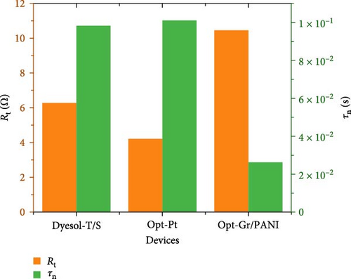
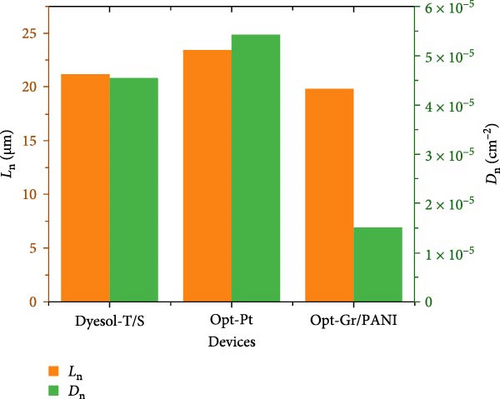
Furthermore, Figure 8’s left vertex indicates the trend of Ln which is the most important parameter to optimize film thickness since higher thickness is required for large amount of dye accommodation. It shows that Opt-Pt has clearly higher Ln than control and Opt-Gr/PANI device; Opt-Pt device shows the diffusion length of 23.4 µm which is quite appropriate for large amount of dye adsorption. The right vertex of Figure 9 shows the trend of Dn; Opt-Pt has shown significantly higher Dn than both the control and Opt-Gr/PANI. It has been seen that all electron transport parameters are favorable for Opt-Pt devices which are in line with photovoltaic performance. It can be explained with the help of schematic illustration given in Figure 5’s inset that graphene in TiO2 matrix generates impurity state (B) between CBs and VB; this accelerates charge transfer and reduces recombination. The reduction in band gap as depicted in the analysis of optical properties is the evident of the impurity state appearance [43].
6. Conclusion
In this work, graphene-incorporated TiO2 blocking layer, transparent layer, and scattering based integrated optimized photoelectrode DSSCs have been reported with Pt and graphene/PANI cost-effective counter electrode with relatively large active area of 1 cm2 to evaluate the true potential. The optical properties and EIS analysis have revealed that the optimum components of photoelectrode effectively improved the electron transport properties and enhanced light-harvesting capability of dye. For instance, τn and Dn of Opt-Pt was increased by ~87% and ~20%, respectively, as compared to control devices. Consequently, 5.94% of PCE was achieved, which is 20% higher than devices fabricated based on commercial or control materials (Dyesol-T/S). Moreover, devices with optimized photoelectrode and graphene/PANI cost-effective counter electrode (Opt-Gr/PANI) have shown 4.04% PCE which is ~70% of PCE that was achieved with Pt.
Conflicts of Interest
The authors declare no conflicts of interest.
Funding
This work was supported by Universiti Teknologi PETRONAS, Malaysia, under Research Grant URIF (015LB0-029) and YUTP (015LCO-497) and Chinese Academy of Sciences President’s International Fellowship Initiative (Grant No. 2023VTC0005). The authors thank the Qatar National Library, Qatar, for providing Open Access funding for this work.
Acknowledgments
The authors thank the Qatar National Library, Qatar, for providing Open Access funding for this work.
Open Research
Data Availability Statement
The data will be made available by the corresponding authors upon reasonable request.


