New Non Isolated DC–DC Converter for Photovoltaic Applications: Ultra High Voltage Gain With Current and Voltage Stress Reduction
Abstract
This paper proposes an ultrahigh voltage gain nonisolated DC–DC converter based on a modified double boost mode (MDBM), combined with a modified switched inductor-switched capacitor (MSLSC) technique. The modified voltage multiplier technique (MVMT) is integrated with the MSLSC and MDBM using a second main metal-oxide-semiconductor field-effect transistor (MOSFET) and an auxiliary third MOSFET to achieve ultrahigh voltage gain while reducing voltage stress across power devices. The primary objective is to achieve a voltage gain exceeding 21, thereby minimizing voltage stress on power devices, such as diodes and MOSFETs, as well as reducing current stress on all power switches and diodes in the proposed converter (PC). The MSLSC works in conjunction with the auxiliary third MOSFET and the double main MOSFETs to double the voltage gain and further reduce voltage stress on power devices. Notably, all diodes in the MVMT operate under zero current switching (ZCS), and the double main MOSFETs in the MDBM, along with the auxiliary third MOSFET, experience minimal current stress even at ultrahigh voltage gain levels. This converter offers several advantages, including high efficiency, reduced voltage stress on power devices, and lower current stress on power switches compared to previous nonisolated high step up DC–DC converters. The PC is designed to boost input voltages from 30V to a variable output range of 400–650 V, delivering up to 550 W with a peak efficiency of 96.5%.
1. Introduction
Despite the evident environmental and economic benefits of renewable energy sources, such as photovoltaic (PV) and wind generation, certain limitations hinder their optimal utilization. Among these challenges, low output voltage is a significant concern. To address this issue, high step up DC–DC converters have been developed [1, 2]. However, these converters come with their own set of challenges, particularly regarding input current (Iin) waveform quality and cost-effectiveness in design and operation [3]. This paper explores the intricacies of high-gain DC–DC converters, focusing on factors, such as voltage stress on semiconductor devices, conduction losses, and component count. Additionally, it examines the size of passive components and their impact on output voltage quality. Numerous converter topologies have been proposed in the literature, reflecting ongoing efforts to address these challenges in renewable energy systems (RESs) [4, 5].
Researchers have emphasized high voltage gain DC–DC converters for RES, particularly for low-power applications. One design integrates a switched inductor cell (SLC) with a voltage multiplier cell (VMC) [3, 6]. Active–passive inductor cells (APICs) enhance performance through parallel charging and series discharging of inductors [4, 7]. Innovations include a transformerless, nonisolated converter with continuous Iin and simplified single-switch control [8, 9]. Another design modifies a high-gain DC–DC boost converter with two voltage multiplier cells (VMCs), employing switched capacitors (SC) and switched inductors (SL) [10, 11]. A nonisolated, high ratio step up DC–DC converter minimizes voltage stress and simplifies control [12, 13]. Notably, a high-gain DC–DC boost converter achieves six times the voltage gain of standard converters, leveraging SL and capacitors for enhanced efficiency [14, 15].
In renewable energy applications, a cutting edge interleaved high step up DC–DC converter has been proposed [12, 16]. This design incorporates coupled inductors (CI) and a built in transformer (BIT) with two double-winding (2 W) CIs and one triple-winding (3 W) BIT [16, 17]. Additionally, it employs an interleaved series parallel switched inductor and capacitor configuration [12, 18] to achieve high voltage gain. Building on this [17], introduces an ultrahigh voltage gain converter utilizing interleaving and a 3W CI to reduce filter component size. Voltage stress on semiconductor devices is mitigated by optimizing the CI turn ratio, while the interleaved structure minimizes peak-to-peak Iin variation and reduces switching losses. Complementing these advancements [19, 20], presents a high step up DC–DC converter integrating active SL (ASI), BITs, and multipliers. These features allow precise duty cycle adjustments to achieve high voltage gain in RES applications. While these converters excel in performance, challenges include high component counts, increased parasitic resistance, and reduced efficiency. Larger components are required at low switching frequencies, and efforts to boost voltage gain often lead to higher internal resistance and associated losses [9, 19]. Converters with clamped circuits address voltage spikes [9, 21] but introduce trade-offs, such as efficiency loss and increased costs due to parasitic effects.
Recent modifications include a switched-inductor double-switch DC–DC converter for higher voltage gain [22, 23]. Advanced designs combine active and passive SL, switched capacitor cells, and auxiliary switches to achieve high voltage gain, low duty cycles, and improved efficiency [24, 25]. A high step up, nonisolated DC–DC converter integrates active and passive SLCs to increase voltage gain while minimizing conduction losses [26]. Addressing renewable energy challenges, a transformerless single-switch high-gain DC–DC converter employs a switched capacitor/inductor cell and a voltage multiplier stage. This design offers high conversion ratios, reduced voltage stress, simplified gate drive requirements, and continuous Iin, making it ideal for prolonged solar PV applications [27–29]. However, challenges persist, such as higher conduction and switching losses at increased duty ratios, affecting power density and efficiency, as well as imposing stress on power switches and diodes. Double inductors and low switching frequencies introduce parasitic resistance, further compromising performance.
In step up DC–DC converters, a single-ended primary-inductor converter (SEPIC) converter-based design [21] integrates a discontinuous current quasi-Z-source and switched-capacitor networks to achieve low Iin ripple and a wide voltage gain range. Conversely, a nonisolated high voltage gain DC–DC converter [24] operates in discontinuous current mode with zero current switching (ZCS), offering a wide duty cycle range and high output voltage gain. An impedance network boost converter [28, 30] is proposed for RES, delivering higher voltage gain with a small duty cycle and fewer components. Additionally, a new family of nonisolated boost DC–DC converters [31, 32] reduces component counts and improves voltage/current stress on switches. The Tri-Switching Double Duty Converter (TSDDC) [33] emerges as a high-gain DC–DC boost converter for PV-based direct current (DC) nanogrid applications, integrating step up and maximum power point tracking through a sophisticated control circuit. Despite their advantages, challenges include high current stress on power switches, significant voltage stress on devices, and large space requirements for complex gate control circuits [10, 34].
A nonisolated high-gain, noninverting interleaved DC–DC boost converter employs a unique topology with two inductors and a voltage multiplier technique for substantial gain [16, 23, 35]. A novel boost DC–DC converter based on the voltage lift (VL) technique combines a VL network with a switched capacitor cell [27]. While offering significant voltage transfer gain, these converters still face limitations, such as increased conduction and switching losses at high duty cycles, which impact overall efficiency and adaptability [30, 36].
In this paper, a nonisolated DC–DC converter is implemented to verify ultrahigh voltage gain while reducing current and voltage stress across the power devices. This is accomplished through the integration of an MDBM interleaved with an MVMT and an MSLSC. The primary goal is to attain an exceptionally high voltage gain exceeding 21.5 by combining MVMT with a second main and auxiliary third MOSFET, along with MSLSC, effectively doubling the voltage transfer gain and to reduce voltage and current stress across all power components in the proposed converter (PC). It’s noteworthy that all diodes in the MVMT operate under ZCS, and the double main MOSFETs in the MDBM, along with the auxiliary third MOSFET, experience minimal current stress even at ultrahigh voltage gain levels when the PC delivers 650V at 550 W. The Iin of the PC maintains stability without pulsating at a low duty ratio, making it particularly well-suited for PV applications. The advantages of the PC include its exceptional efficiency at high power density, minimal voltage stress on the second and third MOSFETs, and low current stress on the power switches, compared to previous nonisolated high boosting DC–DC converters. Furthermore, reducing the current stress across all power switches significantly decreases conduction losses, resulting in improved efficiency. Moreover, the voltage stress on all switches remains notably low, resulting in very low switching loss. To maintain a constant output voltage, voltage, and current PI controllers are meticulously designed.
2. The Principal Operation and Structure of the PC
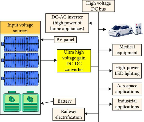
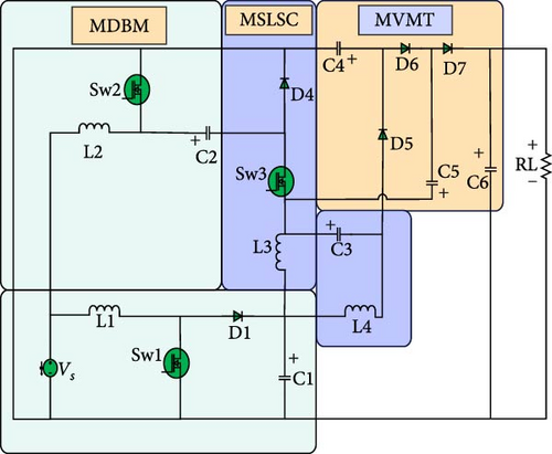
In Figure 1a, the illustration highlights the integration of the PC with solar panels and a battery as low input voltage sources. The PC is connected to a high voltage DC line and various applications, including LED street lighting, electric vehicle (EV) applications, industrial applications, railway electrification, and aerospace applications. Figure 1b presents the circuit diagram of the PC, featuring four small-value inductors, six capacitors, and three power switches (Sw1 as the main switch, Sw2 as the second main switch, and Sw3 as the auxiliary third switch), along with five power diodes. The design of this circuit aims to offer several notable advantages. A key feature of this converter is its ability to eliminate the need for isolated CI and transformers, typically essential for voltage step up. The efficiency of the PC can be significantly improved by operating at a high switching frequency, leading to a reduction in the values of inductors and capacitors. The implementation of the PC structure is intended to be straightforward, with all switches turning on and off simultaneously. This design greatly enhances reliability, especially in PV applications, as the Iin exhibits very low duty cycles with zero pulsation. Addressing concerns about voltage across both the double primary and third switches, as well as all diodes, is a notable feature of the PC. The inductors face low voltage stress at high voltage gain, and the current stress through both the double main and third auxiliary switches is intended to be reduced when the PC supplies 550 W at a 650 V output voltage, with Vs equal to 30 V. The PC aims to achieve superior voltage gain compared to earlier DC–DC converters while utilizing a minimal number of capacitors and inductors. The control mechanism is streamlined by the synchronous turning on and off of three power devices, contributing to the overall efficiency and effectiveness of the PC. Additionally, the gate control circuit is designed to be simple and compact in size.
2.1. Operation of the PC
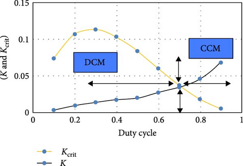
The PC operates in two distinct modes to cater to varying load conditions. The first is the Discontinuous Conduction Mode (DCM), which is employed for light load applications characterized by low duty cycles, specifically those below 70%. In contrast, the Continuous Conduction Mode (CCM) is activated for higher load situations, marked by duty cycles surpassing 70%.
2.2. Operation of the PC at DCM
-
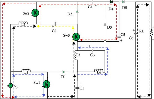
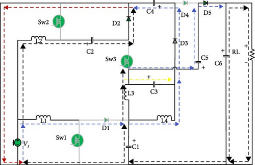
Mode 1: (0–t0): Three MOSFETs—Sw1, Sw2, and Sw3—are in the on state. During this phase, L1 and L2 begin to charge energy from the input source Vs. Simultaneously, L3 and L4 start accumulating energy from C1, which is in series with them. C2 discharges current through Sw2 and this current flows from both L2 and C2 during this mode. C4 and C5 are in series, both discharging energy through Sw3 to keep D4 in the on state. C6 discharges its energy to supply current to the load. The PC for this mode is shown in Figure 2 (a). In addition, diodes D1, D2, D3, and D5 are in the off state during this mode. C3 discharges energy through Sw3 and has the same current as L4. The equations during Mode 1 are as follows:
-
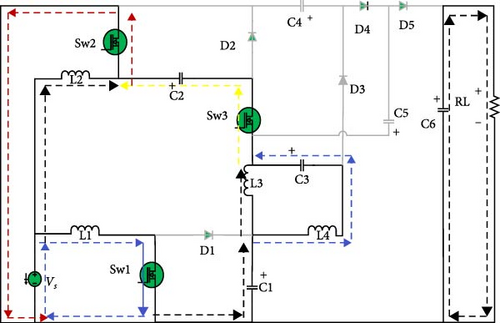
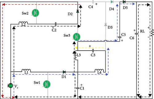
Mode 2: (t0-t1): Three MOSFETs—Sw1, Sw2, and Sw3—are still in the on state. C4 and C5 have zero charges after time (D–A), at which point D4 operates at ZCS as shown in Figure 3a. During this phase, L1 and L2 continue to charge energy from Vs. Simultaneously, L3 and L4 accumulate energy from C1. C6 still discharges its energy to supply current to the load. The current through Sw3 comes from C1 only, leading to a reduction in the current through Sw3 during this mode. Furthermore, the current through Sw2 also decreases after the reduction in Sw3 current. The PC for this mode is depicted in Figure 2b. After the reduction in C2 current, this approach is designed to decrease current stress on both Sw3 and Sw2, enhancing the overall performance of the PC. Additionally, conduction loss of power devices will be significantly reduced during this mode.
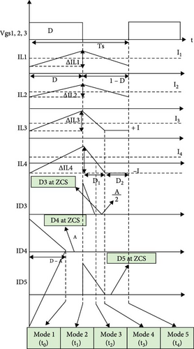
This current stress reduction allows the PC to provide ultrahigh voltage gain with a smaller volume of a heat sink in the PC, thereby significantly reducing its size. All diodes are in the off state during this mode, as illustrated in Figure 3a). D4 operates at ZCS during time (D–A), where, the value of A can be found in Equation (5). The equations during Mode 2 are as follows:
-
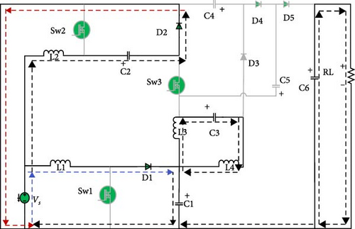
Mode 3: (t1–t2): Three MOSFETs—Sw1, Sw2, and Sw3—are turned off, and diodes D1 and D2 are turned on, while D4 is in the off state. During this phase, L1 releases energy to turn on D1, and L2 releases energy to charge C2 through D2. Additionally, L1 supplies current to L3 and L4, adding C1 current during this mode to supply current to the load after making D5 on state with C5 charging. Moreover, L4 current charges C4 to turn on D3 during this mode, as shown in the circuit diagram of the PC in Figure 2c. Simultaneously, L3 supplies current to charge C3 and to the load with the additional current from L1 with charging C6. This implies that D3 and D5 are in the “on” state. The equations during Mode 3 are as follows:
-
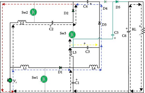
Mode 4: (t2–t3): Three MOSFETs—Sw1, Sw2, and Sw3—are still turned off, and C4 has zero charge during this mode. L3 and L4 charge C5 to supply current to the load and charge C6 through D5. Diodes D1 and D2 remain turned on, while D3 and D4 are in the off state. L1 continues to discharge energy to charge C1 through D1 and supply current to the load by adding the current of L3 and L4, as shown in the circuit diagram of the PC in Figure 2d. Simultaneously, L2 releases energy to charge C2 through D2. Additionally, L4 and C3 share the same current, with C3 discharging energy to the load and charging C6. D3 is in the off state during this phase after time A/2. This implies that D3 is in the “off” state, and both will operate under ZCS at A/2. The current equations during Mode 4 are as follows:
-
Mode 5: [t3–t4]: Three MOSFETs—Sw1, Sw2, and Sw3—are still turned off, and diodes D1 and D2 remain turned on, while D3, D4, and D5 are in the off state. L1 continues to discharge energy to charge C1 through D1, and L2 continues to discharge energy to charge C2 through D2. Meanwhile, L3 and L4 share the same charge current from L1 at D2 but in the reverse direction, along with the same current of C3. Additionally, C6 supplies current to the load. This means all diodes in the MVMT are in the off state when the PC supplies 550 W at a 650 V output voltage. Consequently, the PC operates at high performance and efficiency in high load applications. The configuration of the PC in this mode is displayed in Figure 2e. Notably, the equations are the same as in the previous mode.
Figure 3a provides a visual representation of the five operating modes of the PC DCM, outlining the distinctive characteristics of each mode. Additionally, the corresponding current waveforms of the PC in DCM are depicted to offer a comprehensive understanding of its behavior during this operational state.
Consequently, when the PC functions in DCM, it delivers a substantial load voltage of 650 V at 550 W. In this operating mode, all MVMT diodes engage in ZCS, mitigating current stress and minimizing conduction losses stemming from diode internal resistance. Notably, the stress on Sw1, Sw2, and Sw3 is significantly reduced as the PC attains ultrahigh voltage gain. Furthermore, the voltage stress on all power diodes and switches experiences a notable decrease at Vo = 650 V under high load power conditions. This signifies that the PC can operate with exceptional efficiency and performance. Moreover, the system’s Iin remains stable without pulsations at low duty cycles, rendering the PC particularly well-suited for PV applications.
2.3. The PC Operation in CCM
-
Mode 1: This mode is similar to mode 1 in DCM
-
Mode 2: This mode is similar to mode 2 in DCM
-
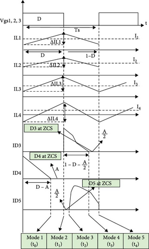
Mode 3: (t1–t2): Three MOSFETs—Sw1, Sw2, and Sw3—are turned off, and diodes D1 and D2 are turned on, while D4 is in the off state. During this phase, L1 releases energy to turn on D1, and L2 releases energy to charge C2 through D2. Additionally, L1 supplies current to L3 and L4, adding C1 current during this mode to supply current to making D3 in the on state with C4 charging, as shown in the circuit diagram of the PC in Figure 2f. While D5 is in the off state during this mode at A/2, meaning D5 will operate under ZCS at A/2. C6 still supplies a high load current to the load at a high switching frequency. The equations during Mode 3 are the same as in the previous mode.
-
Mode 4: (t2–t3): This mode is similar to mode 3 in DCM
-
Mode 5: (t3–t4]: This mode is similar to mode 4 in DCM
3. Voltage Gain at CCM
Equation (18) serves as a representation of the output voltage of the PC, achieved by summing Equations (15) and (16). The depiction of the voltage gain equation for the PC in CCM is encapsulated in Equation (18). It’s noteworthy to emphasize that the PC exhibits a notably superior voltage gain when compared to its predecessors.
4. Voltage Gain at DCM
Figure 4 illustrates the dynamic performance of the PC in both CCM and DCM. It is evident that, based on the condition outlined in Equation (28), when the duty cycle is below 0.7, the PC operates in DCM. On the flip side, as the load current rises and the duty cycle surpasses 70%, the PC transitions into CCM.
5. Voltage Stress Analysis
6. Components Design and Total Cost of the PC
The essential components of the 550 W prototype for the PC include capacitors, inductors, MOSFETs, and power diodes. Achieving a high voltage gain requires careful design of these components. The PC comprises four inductors with small values and six capacitors with small values, as outlined in Table 1, providing clarity on the prototype design parameters.
| Parameters | Values |
|---|---|
|
|
| SiC Schottcky diodess | 650 V, 40 A, (IDW20G65C5) |
| L1 = L2 | 150 uH, 3 mΩ |
| L3 = L4 | 100 uH, 1.85 mΩ |
| C1 = C2 | 100 uF, 100 V |
| C3 | 3.3 uF, 220 V |
| C4 = C5 | 100 uF, 500 V |
| C6 | 74 uF, 900 V |
| Vo | 400–650 V |
| Vs | 30 V |
| fs (switching frequency) | 150 KHZ |
| D duty cycle | 46% at 650 V output voltage |
| Power | 550 W |
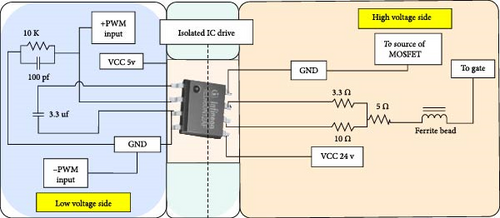
| Ic drive circuit | 1EDI60N12AF |
| Current sensor | HNC-05SY |
| Voltage sensor | LEM LV25-P |
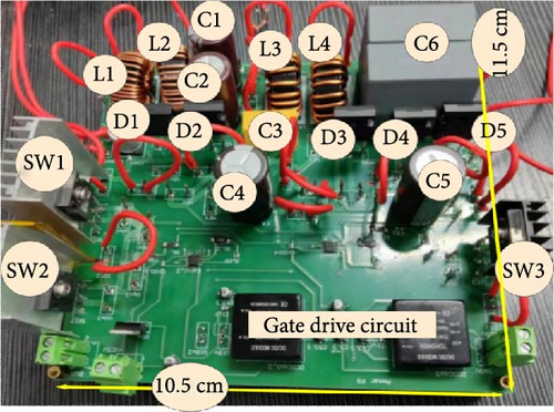
| The proposed converter size | L = 11.5 cm, H = 4.45 cm, and W = 10.5 cm |
| Power density | 1.01 (w/cm3) |
Table 1 emphasizes a significant reduction in inductor values as switching frequencies increase. Moreover, the inherently low internal resistance of these inductors plays a crucial role in minimizing power losses within the PC. In the process of designing the inductors for the 550 W PC, Equation (40) for L1 and L2, along with Equation (41) for determining the critical value of L3 and L4, are integral. The calculation of capacitor values is accomplished through Equations (42)–(46). Remarkably, Table 1 highlights the effectiveness of employing toroidal core inductors with dimensions (L = 2.5 cm, H = 2.5 cm, W = 1 cm) at an exceptionally high switching frequency, resulting in remarkably low internal resistance for the inductors.
In terms of the cost calculation for the PC, Table 2 shows that the estimated cost is almost $40 USD. This represents a very low price, validating the achievement of ultrahigh voltage gain at a low duty cycle with high efficiency and power density.
| SiC MOSFET (TW048N65C) | 3 | 2 | 6 |
| SiC diodes, (IDW20G65C5) | 5 | 1.5 | 7.5 |
| Inductors with toroidal core (L1, L2, L3, L4) | 4 | 1 | 4 |
| Capacitors (C1, C2, C4, C5) | 4 | 1 | 4 |
| Capacitor (C3) | 1 | 0.58 | 0.58 |
| Capacitor (C6) | 2 | 1.5 | 3 |
| Ic drive circuit with components, 1EDI60N12AF | 2 with all (components SMD) | 4.5 | 9 |
| Printed PCB | 1 | 6 | 6 |
| Total price | 40 $ | ||
7. The PC With Control Strategy
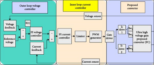
A pair of proportional integral (PI) controllers, as illustrated in Figure 5a, are employed to ensure the optimal performance of the PC. The first PI controller acts as an internal controller, ensuring stable load current, while the second PI controller serves as an outer controller, overseeing the desired output voltage. The error, E(t), which results from subtracting the actual output voltage from the target voltage, serves as the input for the first PI voltage controller. The output of the PI voltage controller determines the reference current for the load, with intentional restrictions in place to prevent excessive current draw. The feedback current is then subtracted from the limited reference current, forming the input for the PI current controller, as governed by Equation (47). To implement this control strategy, an Arduino Uno is used as the controller for the PC, along with the voltage and current sensors listed in Table 1-1.
7.1. Performance Comparison of the PC With Previous High-Gain Converters
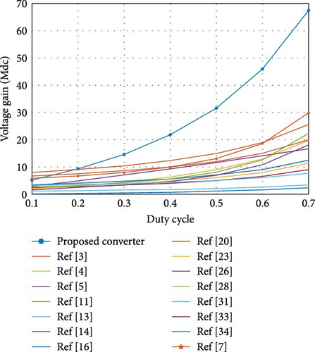
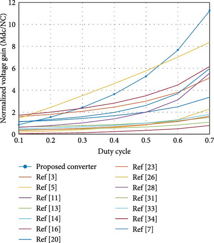
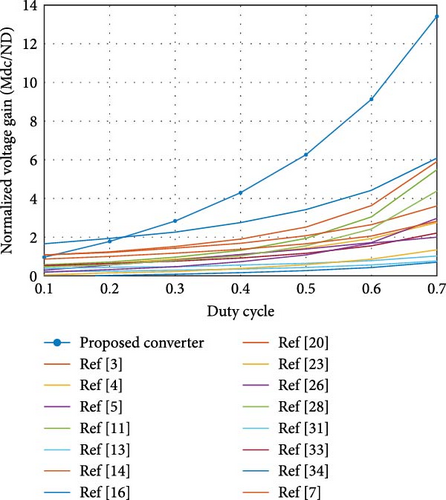
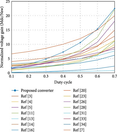
A comparative analysis has been conducted between the PC and its precursors among DC–DC converters. Previous high-gain converters underwent simulation in MATLAB software under identical conditions. In Figure 6a, it becomes apparent that the PC achieves superior voltage gain compared to prior boosting converters. This heightened gain at a low duty cycle signifies a reduction in conduction and switching losses, leading to enhanced efficiency. Observing Figure 6a, it is evident that the PC can provide a high output voltage by stepping up a low input voltage, equivalent to 30 V (Mdc is 21.6). Moreover, it is noticeable that the PC can deliver a higher voltage gain when the duty cycle is ~0.3, as depicted in Figure 6a. Moving to Figure 6b, the PC is demonstrated to exhibit a higher gain compared to its predecessor, once again with fewer counts of capacitors. Figure 6c reveals that the PC achieves a higher gain than the previous converter, with a lower count of power diodes. In Figure 6d, the PC is demonstrated to have a higher gain compared to its predecessor, again with fewer inductors. Figure 6e showcases that the PC achieves a higher gain than the previous converter, with a reduced number of power switches. Notably, all power switches in the PC operate in unison. The PC attains a higher efficiency of 96.1% compared to previous converters. Furthermore, it is evident that the PC can achieve higher efficiency than previous DC–DC converters, with all power diodes operating at ZCS. The current stress on all power switches is significantly reduced at Vo = 650 V and 500 W. Additionally, all power switches turn on and off simultaneously without any complexity in the circuit of the control signal. Moreover, the three power switches are Silicon Carbide (SiC) MOSFETs with low on-state resistance at high switching frequency. This implies that the PC voltage gain is higher than the previous converter, with low conduction and switching losses.

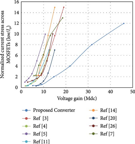
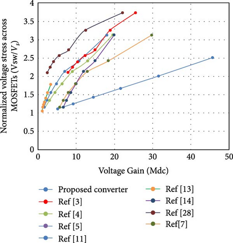
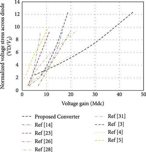
In Figure 7a, it is evident that the stress current passing through the MOSFETs in the PC is notably lower than the current stress experienced by the power switches in previous boosting converters. Furthermore, referring to Figure 8c, d, the current stress across Sw1 is 15 A, Sw2 is 20 A, and Sw3 is 10 A when the PC supplies power at 550 W with Vo = 650 V. This indicates a significant reduction in stress current through both the main and auxiliary third switches at Vo = 650 V, surpassing the levels observed in power switches of previous DC–DC converters. Shifting attention to Figure 7b, it becomes apparent that the power switch devices in the PC undergo lower voltage stress compared to their counterparts in the previously mentioned converters. Additionally, low voltage stress across power switches translates to reduced switching losses, contributing to an overall increase in the efficiency of the PC. Examining Figure 7c, it is evident that the voltage stress on the diode in the PC is lower than in previous converter designs. The voltage across all diodes in the PC exhibits low voltage stress when supplying Vo = 650 V. This implies diminished voltage stress on power diodes, resulting in a reduced need for heat sinks and a more compact size for the PC.

In Table 3, the PC operates at a higher switching frequency, enabling the use of smaller components and minimizing parasitic resistance. This results in a system that is not only compact and lightweight but also cost-effective. Unlike its predecessors, the PC excels in both size efficiency and cost-effectiveness.
| Items | PC | Ref [3] | Ref [4] | Ref [5] | Ref [14] | Ref [18] | Ref [9] | Ref [37] | Ref [15] | Ref [21] | Ref [24] | Ref [26] | Ref [29] | Ref [31] | Ref [32] | Ref [33] | Ref [7] |
|---|---|---|---|---|---|---|---|---|---|---|---|---|---|---|---|---|---|
| FS (kHz) | 150 | 20 | 20 | 50 | 20 | 20 | 50 | 24 | 50 | 100 | 1 | 100 | 31.3 | 50 | 50 | 50 | 50 |
| Vs | 30 | 24 v | 20 | 20 | 15 | 48 | 20 | 20 | 16 | 300 | 24 | 15 | 20 | 25 | 48 | 21 | 48 |
| Vo | 400–650 | 240 | 160 | 200 | 183 | 178 | 299 | 172 | 150 | 800 | 221 | 384 | 200 | 200 | 408 | 400 | 650 |
| NL | 4 | 4 | 6 | 5 | 2 | 4 | 2 | 3 | 2 | 3 | 4 | 2 | 2 | 2 | 2 | 4 | 2 |
| NC | 6 | 5 | 1 | 8 | 4 | 3 | 6 | 3 | 6 | 7 | 2 | 4 | 5 | 5 | 2 | 3 | 5 |
| ND | 5 | 7 | 14 | 6 | 5 | 4 | 7 | 3 | 7 | 4 | 8 | 4 | 7 | 4 | 2 | 9 | 5 |
| NSW | 3 | 2 | 2 | 1 | 1 | 4 | 1 | 1 | 1 | 1 | 2 | 2 | 1 | 1 | 2 | 3 | 2 |
| Duty cycle (%) | 45 | 27 | 60 | 60 | 60 | 65 | 60 | 70 | 45 | 60 | 42 | 77 | 50 | 72 | 73 | D1 = 50D2 = 30 | 66 |
| Power (W) | 500–550 | 120 | 200 | 200 | 176 | 130 | 250 | 100 | 200 | 1000 | 200 | 200 | 150 | 200 | 425 | 400 | 400 |
| Input current pulsating | No | Yes | Yes | No | No | No | Yes | No | Yes | No | Yes | Yes | No | No | No | Yes | yes |
| Efficieny (%) | 96.1 | 95.5 | 95.5 | 90 | 92 | 92.5 | 91 | 91.4 | 94.7 | 95 | 93 | 94.2 | 94.5 | 94.2 | 92 | 94 | 95 |
| Mdc | |||||||||||||||||
| Power density (W/cm3) | 1.01 | — | — | 0.71 | — | — | — | — | — | — | — | 0.35 | — | — | — | — | 0.71 |
| Cost/($) | 40 | — | — | — | — | — | — | — | — | — | — | — | — | — | — | — | 120 |
While earlier converters achieved high voltage gain through a high-duty cycle, the PC efficiently elevates low Vs to a variable Vo (ranging from 400 to 650 V) with a low (D). Additionally, it features fewer power diodes, all operating under ZCS, thereby reducing losses from forward voltage and internal resistance. Regarding Iin, the PC maintains stability with zero pulsation at both low and high-duty cycles. Table 3 illustrates that the PC exhibits higher efficiency compared to previous converters. Furthermore, it boasts a higher power output than the previous work. In terms of gate control (refer to Figure 1b), all power MOSFETs switch on and off simultaneously with a simple gate control circuit. In contrast, the gate control circuit in [33] is quite complex, involving two different duty cycles to achieve high voltage gain. Examining the voltage gain equation, it is evident that the PC achieves a higher gain than previous converters at D = 0.45. This suggests that the PC is well-suited for applications requiring variable and fixed high output voltages across a wider range of duty cycles, achieving an impressive efficiency of 96.1%. In terms of power density, the PC surpasses the previous work. Additionally, the total cost of the PC is lower than that in [7].
8. Efficiency Calculation of the PC
To ascertain the current stress on power switches, Equations (48)–(50) are employed to calculate the root mean square (rms) current flowing through Sw1, Sw2, and Sw3 respectively. It can be observed from Equations (49) and (50) that the stress current through Sw2 and Sw3 is significantly reduced when the PC delivers 550 W at a 650 V output voltage. Additionally, the stress current through Sw2 and Sw3 depends on the value of A, which can be calculated using Equation (5).
Equations (58)–(63) present the effective current through capacitors. It can see that the rms current through C4 and C5 are function of A, where A can be found in Equation (5).
8.1. Losses Calculation for MOSFET Devices
To analyze the power losses in power MOSFETs, we classify them into two types: conduction and switching losses. Equation (64) is employed to calculate MOSFET power conduction losses (Pcd), while Equation (65) is utilized to determine power switching losses (PSW) incurred by the MOSFETs. In these equations, Coss represents the MOSFET output capacitor, and Fs denotes the switching frequency. The comprehensive evaluation of switch power loss is encapsulated in Equation (66), identified as MTL. This equation integrates both Equations (64) and (65), offering a holistic perspective on the overall power losses of MOSFETs in the PC.
8.2. Losses in Power Diode
8.3. Losses in Inductors and Capacitors
8.4. Total Power Losses in the PC
In Figure 9a, the advantageous integration of toroidal core inductors with low internal resistance emerges as a pivotal factor in achieving a noteworthy reduction in the overall power loss within the PC system. This strategic implementation results in enhanced efficiency and performance. Notably, the incorporation of cutting edge components, including SiC (MOSFETs), SiC diodes, and capacitors characterized by low resistance, further amplifies the efficiency of the PC.
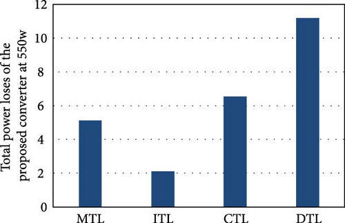
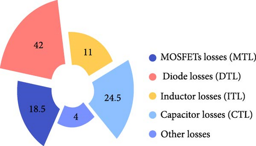
The PC undergoes a transformative improvement with the introduction of novel combined techniques, particularly discernible in the performance when supplying 550 W. This innovation manifests in a discernible decrease in current stress experienced by D3, D4, and D5. The consequential effect is a notable enhancement in both efficiency and overall system performance. Moving on to Figure 9b, a comprehensive analysis reveals that a substantial proportion of power loss can be attributed to the capacitors and diodes within the system. Moreover, intrinsic resistance within the inductors and power switches also contributes to the overall losses experienced by the system, with low percentages of 11% and 18.5%, respectively. This detailed examination sheds light on critical areas that can be targeted for further optimization and refinement in future iterations of the PC design.
9. Experimental Results and Discussions
Experimental results for the PC were validated using a 550 W PCB prototype, as illustrated in Figure 10. Rigorous quality validation and robustness assurance were attained through the use of simulation tools like MATLAB Simulink and PLECS software, ensuring results were verified across diverse scenarios. This comprehensive approach served to reinforce the effectiveness of the converter.
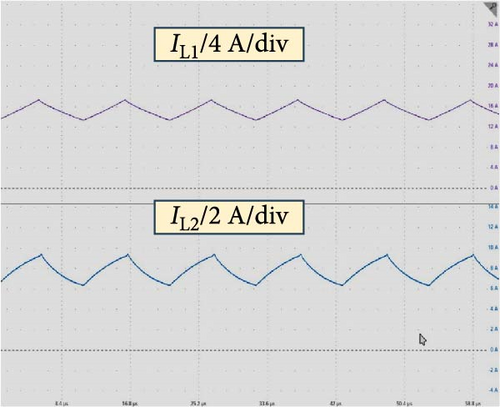
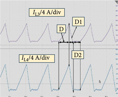
In Figure 11a, the inductor currents, IL1 and IL2, are observed as the PC is operated in DCM mode at a 650 V output voltage and 500 W power with a duty cycle of 45%. In Figure 11b, the inductor currents, IL3 and IL4, are observed as the PC operates in DCM mode at Vo = 650 V.
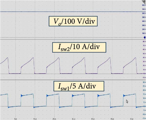
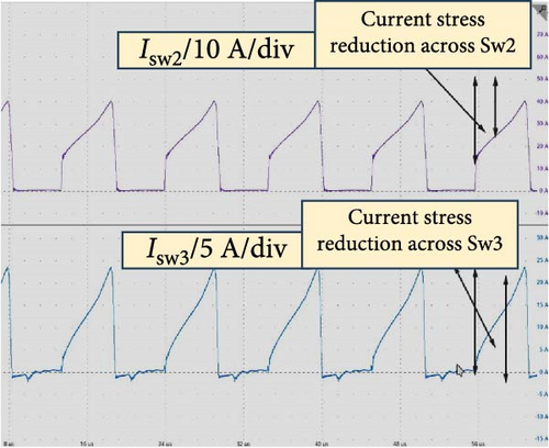
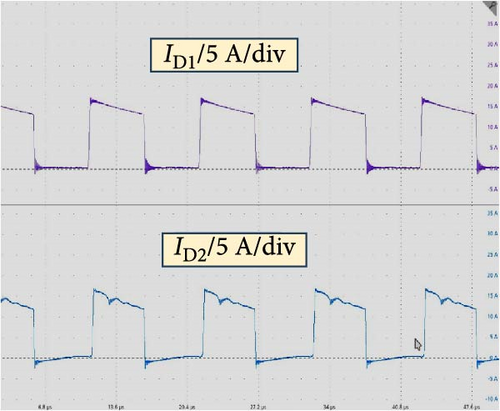
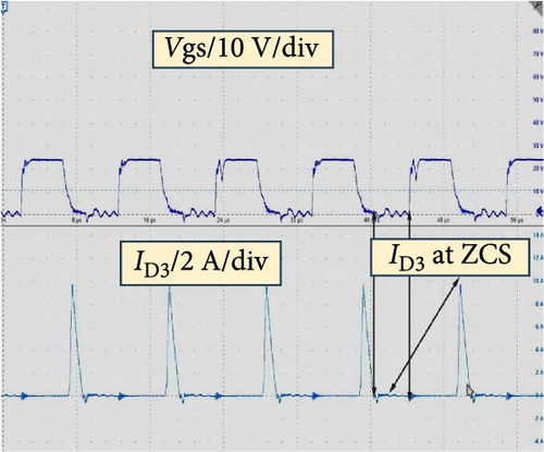
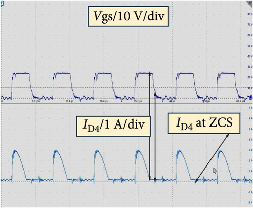

In Figure 11c, d, the currents through Sw1, Sw2, and Sw3 are seen. These currents are significantly lower when the PC supplies a 500 W load, indicating a substantial reduction in conduction losses of three MOSFETs, leading to improved performance and efficiency for the PC. The average currents of Sw2 and Sw3 are found to be equal to 20 and 10 A, respectively. In Figure 11e, the current through D1 and D2 is observed with low stress current across them when the PC provides 500 W. Figure 11f shows the current through D3, where it operates under ZCS. Figure 11g displays the current through D4, operating under ZCS. Figure 11h illustrates the ID5, also operating under ZCS.
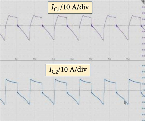
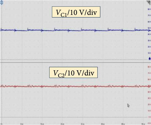
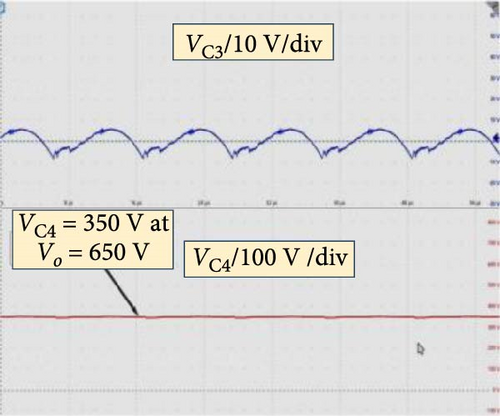
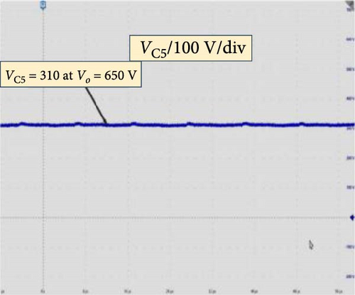
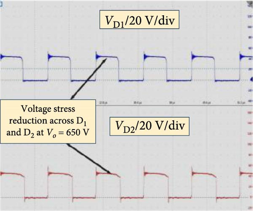
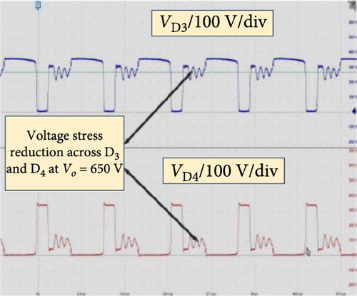
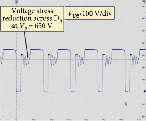
In Figure 8a, the current through C1 and C2 is observed when the PC supplies 500 W at a duty cycle of 45%. In Figure 8b, the current through C3 and C4 is shown when the PC supplies 500 W, where the current through C3 and C4 are the same but in reverse direction and equal to zero during the off state (D-A). Figure 8c shows the Vc1 and Vc2, respectively, equal to 60 V. Figure 8d shows the voltages across C3 and C4, respectively, where the average voltage across C3 is equal to zero, and the VC4 is equal to 350 V. Figure 8e shows the Vc5 at 310 V. The output voltage of the PC is the sum of VC5 and VC4, totaling 660 V. Figure 8f shows that the VD1 and VD2 is kept considerably low, equal to 56 V at the off state. Figure 8g shows the VD3 and VD4, which is a very low voltage. In Figure 8h, the VD5 shows significant reductions when the PC operates at a high voltage gain of 650 V, where the voltage across the diodes is almost half of the output voltage.
Figure 12a displays the Vsw1 and Vsw2, which are very low and equivalent to Vc1 and Vc2, respectively. Figure 12b shows the Vsw3, observed to be equal to 292.5 V with low voltage switching when the PC operates in DCM at Vo = 650 V at 500 W.
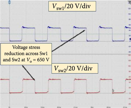
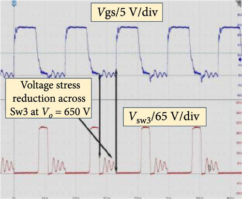
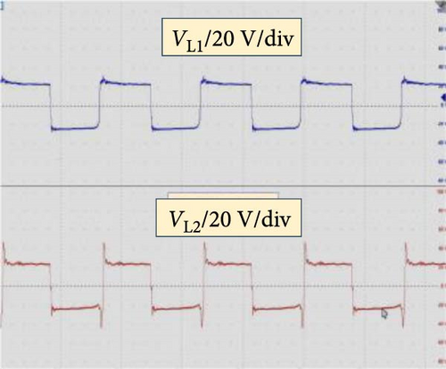
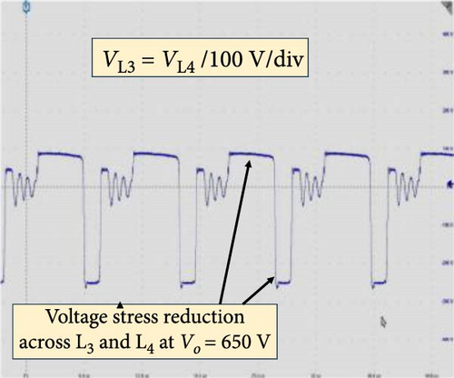
This implies that the power devices’ voltage stress is considerably diminished when the PC operates at a high output voltage. Consequently, the power MOSFETs’ switching losses are greatly minimized, enabling the PC to operate with high efficiency and performance. Figure 12c displays the voltage across inductors L1 and L2, equal to the input voltage source set at 29 V with an output voltage of 650 V.
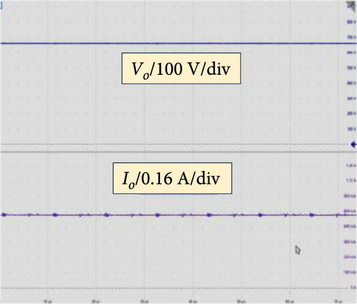
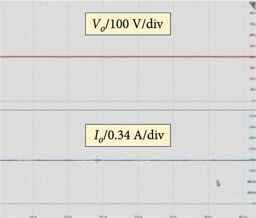
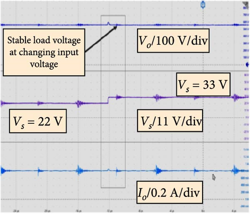
Figure 12d shows the voltage across inductors L3 and L4, remaining at 120 V during the on state, equivalent to (VC1 + VC2). In Figure 12e, f, it is observed that the PC can supply 500 W at a high output voltage. Additionally, the load voltage is maintained at 650 V with a load current of 0.765 A at Vs = 29 V with gain Mdc = 22.4. It can be seen that the PC can supply 400 V at 550 W with a load current of 1.37 A. Figure 12g indicates that the Vo and load current of the proposed topology remains constant when the Vs changes from 22 to 33 V after applying a dual PI controller.
As result, the analysis of Figures 8, 11, and 12 provides a comprehensive understanding of the PC’s performance under different operating conditions. The inductor currents, switching currents, and voltages across various components demonstrate the PC’s ability to operate efficiently and with reduced stress on power devices, especially at a high output voltage of 650 V. The significant reduction in conduction losses of MOSFETs, low stress currents across diodes, and the ability to supply 500 W at 650 V highlight the improved efficiency of the PC. Moreover, the PC exhibits stable operation with varying loads, showcasing its versatility and performance at different power levels. Overall, the findings suggest that the PC is well-designed for high efficiency power supply applications, offering improved performance and reduced stress on components.
The converter adeptly steps up a 29 V input to a 650 V output under a 550 W load with gain Mdc = 22.4, effectively alleviating stress on all diodes in MVMT. All diodes in MVMT achieve ZCS at specific intervals, optimizing performance. To minimize current through Sw2 and Sw3, the stress on these switches diminishes as capacitor C4 and C5 charges reach zero. The voltage stress on power diodes, MOSFETs, and inductors markedly decreases with Vo = 650 V at 550 W, resulting in a substantial reduction in switching and conduction losses for power devices. This, in turn, leads to a significant boost in efficiency. In essence, the PC operates at elevated levels of efficiency during high load conditions.
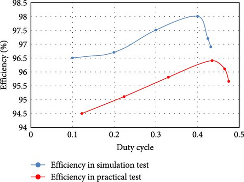
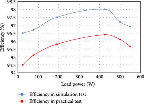
In Figure 13a,b, it’s evident that the PC exhibits high efficiency, reaching 96.1% at a load voltage of 650 V and a load current of 500 W. Notably, the PC maintains an impressive efficiency of 96.1% with a duty cycle of 45% under the same load conditions. It’s essential to highlight that the inductors used in the design of the PC are constructed with flat wire, boasting exceptionally low internal resistance. Additionally, SiC MOSFET devices, renowned for their low internal resistance (Ron), have been strategically incorporated into the converter’s design. Furthermore, SiC diodes featuring low forward voltage (Vf) have been chosen to validate the high voltage gain achievable with this converter while maintaining high efficiency. Moreover, it’s worth noting that the Iin of the PC exhibits minimal pulsation across a wide range of duty cycles, making the system exceptionally well-suited for integration into RESs. The incorporation of the ZCS technique in the PC significantly contributes to its ability to operate efficiently and deliver outstanding performance. The converter efficiently steps up a 30 V input to 650 V output under a 550 W load, notably reducing stress on all diodes in TB technique.
10. Conclusion
In conclusion, the nonisolated DC–DC converter presented in this study embodies innovation and efficiency in power electronics. By combining a MSLSC and a MDBM, the converter achieves an extraordinary voltage gain exceeding 22.4. This accomplishment translates to reduced voltage stress on critical power components, such as diodes and MOSFETs, while simultaneously minimizing current stress on the main power switches and diodes within the MVMT. The interleaved design of the MVMT with the second main and auxiliary third MOSFETs, along with the MSLSC, ingeniously doubles the voltage transfer gain, showcasing the converter’s prowess. Operating under ZCS, all diodes in the MVMT contribute to the overall efficiency of the system. The collaboration between the MSLSC and the auxiliary third and double main MOSFETs results in a doubled voltage gain, with minimal current stress even at ultrahigh levels. The converter exhibits exceptional performance, stepping up a 29 V input to a variable output range of 400–650 V, delivering 550 W at an impressive efficiency rate of 96%. With its steady Iin flow and low pulsations at a low duty ratio, the converter emerges as a fitting solution for integration into RESs. The incorporation of advanced technologies, such as flat wire inductors and SiC MOSFET devices further underscores its commitment to efficiency and performance. In essence, this converter not only meets but surpasses the demands of high load conditions, making it a noteworthy advancement in the realm of power electronics.
As future work, optimization algorithms, such as Particle Swarm Optimization (PSO) will be employed to optimally select the proportional (Kp) and integral (Ki) controller parameters. Additionally, advanced control techniques, including model predictive control, sliding-mode control, and enhanced state space averaging methods, will be explored to improve the dynamic response, minimize ripple, and enhance performance under fluctuating load conditions.
Conflicts of Interest
The authors declare no conflicts of interest.
Funding
The authors extend their appreciation to the Deanship of Research and Graduate Studies at King Khalid University for funding this work through large research project under Grant RGP.2/569/46.
Acknowledgments
The authors extend their appreciation to the Deanship of Research and Graduate Studies at King Khalid University for funding this work through large research project under Grant RGP.2/569/46.
Open Research
Data Availability Statement
Data sharing is not applicable to this article as no new data were created or analyzed in this study.


