Volume 2025, Issue 1 5517224
Research Article
Open Access

Synergistic Effects of Nitrogen–Oxygen–Nitrogen, Forming Gas–Oxygen–Forming Gas, and Argon–Oxygen–Argon Annealing Ambient on the Structural and Electrical Characteristics of Thulium Oxide Passivation Layers on Silicon Substrate

Junchen Deng

Junchen Deng

Institute of Nano Optoelectronics Research and Technology (INOR) , Universiti Sains Malaysia , 11800 , Penang , Malaysia , usm.my

Bailie School of Petroleum Engineering , Lanzhou City University , Lanzhou , 730070 , China , lzcu.edu.cn

Search for more papers by this author
Hock Jin Quah

Corresponding Author

Hock Jin Quah

Institute of Nano Optoelectronics Research and Technology (INOR) , Universiti Sains Malaysia , 11800 , Penang , Malaysia , usm.my

Search for more papers by this author
First published: 02 February 2025
Citations: 1
Academic Editor: Sejoon Lee

Abstract

A comprehensive probe was conducted to compare the impact of postdeposition annealing at 700°C in different ambient of nitrogen–oxygen–nitrogen (NON), forming gas–oxygen–forming gas (FGOFG), and argon–oxygen–argon (ArOAr) on the passivating characteristics of thulium oxide (Tm2O3) on the silicon (Si) substrate. The nitrogen ions have been incorporated in Tm2O3 passivation layers after annealing in NON and FGOFG ambient, of which NON ambient has impeded the growth of silicon oxide (SiO2) interfacial layer (3.258 nm). Although a thicker SiO2 interfacial layer (4.026 nm) was formed after annealing in FGOFG ambient, the attainment of the highest k value (16.8) indicated that the existence of hydrogen ions has assisted the improvement in the overall k value of Tm2O3 passivation layers. Furthermore, the capacitance–voltage characteristic revealed that the FGOFG ambient was effective in reducing the effective oxide charge (1.32 × 1012 cm−2), while NON ambient was effective in passivating the slow trap density (STD) (3.20 × 1011 cm−2). The Terman, Hill–Coleman, and high–low frequency methods have demonstrated the acquisition of the best interface quality during annealing in FGOFG ambient. As a result, the FGOFG annealing process has led to the maximum breakdown electric field of 4.03 MV/cm and the minimum leakage current density for the Tm2O3 passivation layer.

1. Introduction

With the birth and development of Industry 4.0, almost all aspects of human life and production will be linked together through a range of electronic devices, wherein the silicon (Si)-based metal–oxide–semiconductor (MOS) devices have played an important role in fulfilling the requirement of high-performance and advanced technology [1]. For many decades, Si has stood out from the crowd to be the most widely used semiconductor material due to its low cost and ability of attaining excellent passivating layer through the thermally grown native oxide of Si (silicon oxide [SiO2]) that would ensure the Si-based MOS devices to operate reliably [2]. In order to further enhanced the performance and energy efficiency of Si-based MOS devices, the dimension of Si-based MOS devices has been shrunk throughout the years wherein further reduction in the thickness of SiO2 to the range of 1 nm would result in the intolerable high gate leakage current governed by direct tunneling mechanism [3]. Thus, substituting SiO2 with alternative materials possessing higher dielectric constant (k) could provide similar capacitance with a greater physical thickness that would circumvent the detrimental effect of direct tunneling mechanism, which would further enhanced the performance as well as energy efficiency of Si-based MOS devices [1]. To date, numerous research efforts have been carried out with regard to the employment of various alternative high-k materials, such as HfO2 [4], Al2O3 [5], ZrO2 [6], Ga2O3 [7], Y2O3 [8], CeO2 [9], Yb2O3 [10], La2O3 [11], Ta2O5 [12], and thulium oxide (Tm2O3) [13, 14] which could potentially addressed aforementioned detrimental effects. Out of all these high-k materials, rare earth Tm2O3 has emerged as a promising option for application in Si-based MOS devices as a passivation layer by virtue of intriguing features such as high-k value (9.4–18.0) [1418], wide band gap (Eg) (5.2–6.8 eV) [16, 1921], large conduction band offset with relative to Si (2.00–2.95 eV) [19, 22], and excellent thermal stability with Si [23].

Previous attempts have disclosed that the as-deposited Tm2O3 passivation layers on Si substrate were comprised of a high density of intrinsic defects regarding to the Si dangling bonds and oxygen vacancies formed at the interface [2426]. Similarly to other high-k materials, Tm2O3 has a high coordination number making relaxation as well as reorientation of Tm2O3 bonding to be very challenging unless postdeposition annealing process was employed [3, 27]. Consequently, the postdeposition annealing was performed to decrease the number of defect states in the Tm2O3 passivation layer, giving rise to the improved threshold voltage, carrier mobility, and reliability of the Si-based MOS devices [3, 15, 17, 24, 25, 28]. Different forms of ambient have been used for annealing after deposition process, including oxygen [16, 24, 25, 29, 30], nitrogen [17, 28, 30], argon [31], ozone [30], and forming gas (FG) (a mixture of hydrogen and nitrogen gases) [15, 16, 30] to enhance the passivating characteristics of the Tm2O3 passivation layer, which include the leakage current density, interface quality, and k value. Of this investigated postdeposition annealing ambient, it was found that using an oxygen ambient during annealing at 800°C has helped to low the interface trap density of the as-deposited Tm2O3 passivation layer on Si from 8.1 × 1012 to 1.6 × 1012 cm−2eV−1 [24]. The beneficial impact of the oxygen ambient on interface quality was further confirmed for the Tm2O3 passivation layer on a germanium (Ge) substrate, wherein the oxygen annealing has resulted in a lower interface trap density of 3.7 × 1011 cm−2eV−1 than nitrogen annealing of 8.9 × 1011 cm−2eV−1 at similar annealing temperature of 500°C [30]. Additionally, the compositional homogeneity of the as-deposited Tm2O3 passivation layer was restored when it was subjected to postdeposition annealing at temperatures ranging from 500 to 800°C in an oxygen ambient. The smaller flat-band voltage shift (∆VFB) observed in the annealed samples indicated a lower defect density compared to the as-deposited sample [24]. Nevertheless, one of the hindrance of using oxygen ambient is the acquisition of a higher capacitance equivalent thickness when compared with nitrogen ambient, suggesting the formation of thicker interfacial layer [30]. Further investigation based on X-ray photoelectron spectroscopy core level spectra of Ge 3 p has revealed the increment in ratio between the peak areas associated with GeOx and Ge, which has reinforced the increased formation of the GeOx interfacial layer that likely contributes to the reduction in the overall k value of the Tm2O3 passivation layer [30].

Additionally, the employment of nitrogen or FG (97% nitrogen and 3% hydrogen) during annealing process for Tm2O3 passivation layers has contributed to the acquisition of higher k values of 16 [17] and 18 [15], respectively, when compared with oxygen annealed Tm2O3 passivation layer (k = 14.0–15.0) [16]. Therefore, the annealing process in nitrogen- and/or hydrogen-containing ambient has facilitated in the suppression of oxygen diffusion to the Si/Tm2O3 interface, thereby forming a thinner interfacial layer. Similar results have been observed for the HfO2 passivation layer [32, 33]. Besides, argon gas was also known as an oxygen-deficient ambient that was capable of providing suppressive effect toward the growth of interfacial layer during annealing process [34]. While the growth of interfacial layer was retarded during annealing in an oxygen-deficient ambient, the oxygen-deficient annealing, which includes the nitrogen and FG annealing, may result in a degradation of the interface quality of Tm2O3 passivation layer, whereby a lower interface trap density was attained by Tm2O3 passivation layer annealed in oxygen ambient [30]. This indicated that oxygen ambient was a prerequisite to enhance the interface quality, fix defects associated to oxygen, and restore the compositional homogeneity of Tm2O3 passivation layers [30, 31]. In order to take advantage on both oxygen and oxygen-deficient ambient, the postdeposition annealing was conducted in a combination of nitrogen–oxygen–nitrogen (NON) ambient. Specifically, nitrogen gas was introduced during the heating and cooling phases, while oxygen gas was introduced during the dwelling phase [35, 36]. The beneficial effect of using NON ambient was revealed, whereby the Tm2O3 passivation layer annealed in NON ambient at 700°C has obtained a higher k value of 16.0 [35] when compared with oxygen ambient (k = 14.0–15.0) [16]. Therefore, this research work intends to innovate by performing a systematic investigation on the effects of postdeposition annealing at 700°C in NON [35], forming gas–oxygen–forming gas (FGOFG), and argon–oxygen–argon (ArOAr) ambient on the structural, morphological, optical, and MOS characteristics of the Tm2O3 passivation layers.

2. Experimental Procedure

The 4-inch phosphorus doped (~1015 cm−3) n-type Si (100) wafer (resistivity of 1–10 Ω·cm) was cut into smaller dimension of 1 cm × 1 cm. These samples were cleaned in accordance with the procedures of the Radio Corporation of America (RCA). Subsequently, the native oxide of SiO2 was removed by dipping these cleaned samples in a diluted hydrofluoric solution. These samples were immediately loaded into a radio frequency (RF) magnetron sputtering machine (HVV AUTO A500) for the deposition of Tm2O3 passivation layers on Si substrate. The Tm2O3 sputtering target employed in this study was of 99.99% purity. Initially, the plasma cleaning was performed in argon (Ar; 99.9999%) ambient with flow rate of 15 sccm for 10 min and a working pressure of 7.6 × 10−3 mbar using RF power of 100 W. Then, the shutter of the RF magnetron sputtering machine was opened to allow deposition of Tm2O3 passivation layer to be carried out for 40 min. After the deposition process, the postdeposition annealing was conducted in a horizontal tube furnace at 700°C and atmospheric pressure, with different ambient (NON, FGOFG, and ArOAr). The samples were ramped up from 25 to 700°C at a heating rate of 10° C/min under the flow of N2/FG/Ar gas at 100 sccm. Once the postdeposition annealing temperature has been raised to 700°C, a dwelling time of 30 min was employed with the flow of O2 gas at 100 sccm. Subsequently, the horizontal tube furnace was naturally cooled down from 700 to 25°C under the flow of N2/FG/Ar gas at 100 sccm. In this work, FG with a mixture of 10% of hydrogen and 90% of nitrogen was being used. In order to fabricate into a MOS test structure, aluminum (Al) electrodes with diameter of 0.2 mm were deposited on Tm2O3 passivation layers via a shadow mask using a thermal evaporator machine (AUTO 306), while a blanket of Al was evaporated on the backside of Si substrate with a contact resistivity of 0.12 ± 0.02 Ω·cm2.

Grazing incidence X-ray diffraction (GIXRD) with a step size of 0.05° and a step time of 1.5 s were used to characterize the crystalline phases and orientations of the investigated Tm2O3 passivation layers. The thickness of the Tm2O3 passivation layer and the SiO2 interfacial layer was determined by performing X-ray reflectivity (XRR) on the investigated passivation layers with a step size of 0.01° and a step time of 1.5 s. Both GIXRD and XRR measurements were carried out using Bruker D8 Discover with a Cu Kα radiation (λ = 1.5406 Å) that was operated using operating voltage and current of 40 kV and 40 mA, respectively. Surface morphologies, cross-section images, and atomic percentage of elements of the investigated Tm2O3 passivation layers were obtained using field-emission scanning electron microscopy (FESEM) (FEI Nova NanoSEM 450) that was equipped with energy-dispersive X-ray (EDX) (JSM-6460 LV) spectroscopy. The three-dimensional root mean square (RMS) roughness and topographies of the examined Tm2O3 passivation layers were investigated using atomic force microscopy (AFM) (Dimension Edge, BRUKER). The UV-Vis spectrophotometer (Cary 5000) was employed to measure the diffused reflectance spectra of the Tm2O3 passivation layers. Keithley 4200-SCS parameter analyzer was employed to perform current–voltage (IV) measurements as well as capacitance–voltage (CV) and conductance–voltage (GV) measurements in a frequency ranging from 1 MHz to 10 kHz.

3. Results and Discussion

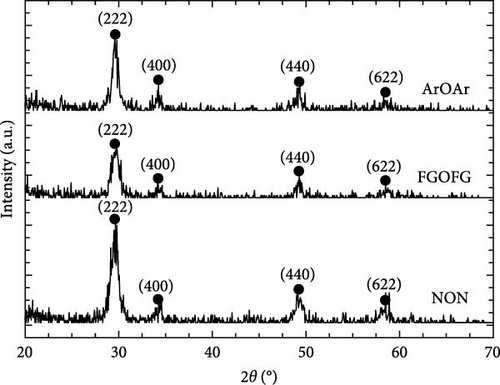
The crystal structure and characteristics of the Tm2O3 passivation layers annealed in NON [35], FGOFG, and ArOAr ambient at 700°C were determined by analyzing the typical GIXRD spectra shown in Figure 1. Polycrystalline phase was observed in all of the investigated Tm2O3 passivation layers. The Tm2O3 phase was oriented in the (222), (400), (440), and (622) planes, which were assigned to the International Center for Diffraction Data (ICDD) file number 00-041-1090 for cubic Tm2O3 phase. Reference to this standard Tm2O3 sample, it was revealed that NON annealing resulted in the least variance in the shifting of detected Tm2O3 peaks to wider diffraction angle. This may imply that nitrogen ions have been incorporated into Tm2O3 lattice and attached to the oxygen vacancies, while the adjacent oxygen ions were released in order to achieve charge compensation. A greater shifting of Tm2O3 diffraction peak was observed for the sample annealed in FGOFG ambient. The observation of larger variation in the shifting of detected GIXRD peaks during annealing in FGOFG ambient could be linked to the existence of both hydrogen and nitrogen gases, wherein the smaller-radius hydrogen ions (0.038 nm) incorporated into the Tm2O3 lattice would contribute to a contraction in the lattice parameter a of the investigated passivation layer [37]. Among these investigated samples, the largest shifting in the detected Tm2O3 GIXRD peaks was observed for the sample annealed in in ArOAr ambient, implying that this sample consisted of a significant number of oxygen vacancies (Table 1).
Details are in the caption following the image
GIXRD patterns of Tm2O3 passivation layers experienced NON [35], FGOFG, and ArOAr annealing at 700°C. ArOAr, argon–oxygen–argon; FGOFG, forming gas–oxygen–forming gas; GIXRD, grazing incidence X-ray diffraction; NON, nitrogen–oxygen–nitrogen; Tm2O3, thulium oxide.
Table 1. GIXRD diffraction angle of Tm2O3 passivation layers experienced NON [35], FGOFG, and ArOAr annealing at 700°C.
Ambient Orientation
(222) (400) (440) (622)
NON 29.598 34.230 49.257 58.497
FGOFG 29.605 34.242 49.270 58.518
ArOAr 29.653 34.273 49.299 58.524
ICDD File No. 00-041-1090 29.475 34.156 49.099 58.312
  • Abbreviations: ArOAr, argon–oxygen–argon; FGOFG, forming gas–oxygen–forming gas; GIXRD, grazing incidence X-ray diffraction; ICDD, International Center for Diffraction Data; NON, nitrogen–oxygen–nitrogen; Tm2O3, thulium oxide.
The lattice parameter a of the investigated Tm2O3 passivation layers was determined according to the fitted results of the obtained GIXRD spectra, as indicated by the following equations [38]:
(1)
(2)
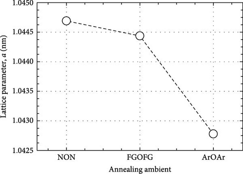
where λ, n, θ, dhkl, and hkl denote X-ray radiation wavelength, diffraction order, diffraction angle, interplanar spacing, and Miller’s index, respectively. All of the investigated samples have attained a smaller a (Figure 2) compared to the standard Tm2O3 sample (1.0487 nm), which has supported the fact that the employment of these annealing ambient (NON, FGOFG, and ArOAr) have triggered a lattice contraction. The lattice parameter was expected to be potentially influenced by the generation of oxygen vacancies and the incorporation of the foreign ions in the Tm2O3 lattice. It was anticipated that the lattice will expand and contract in response to the incorporation of the larger radius nitrogen ions (0.146 nm) and smaller radius nitrogen ions (0.038 nm), respectively [37]. Among the samples analyzed, it has been demonstrated that the Tm2O3 passivation layer, which was annealed in an ArOAr environment, possesses the smallest a (Figure 2). Due to the annealing ambient lack hydrogen and nitrogen ions, the largest lattice contraction observed in this sample was attributed to a significant oxygen vacancies formed after annealing process. Nonetheless, this does not match with the EDX result, which indicates that this sample acquired the highest at% of oxygen (Table 2). One of the possible reasons contributing to this discrepancy was the generation of SiO2 interfacial layer stimulated during annealing in ArOAr ambient, wherein the absence of nitrogen and FG during the heating and cooling stage would cause more oxygen ions to diffuse from the Tm2O3 passivation layer to the Tm2O3/Si interface, forming the SiO2 interfacial layer. Hence, it was postulated that attainment of the highest at% of oxygen for the sample annealed in ArOAr ambient was due to the oxygen ions being accumulated at Si/Tm2O3 interface as well as the oxygen ions from the SiO2 interfacial layer.
Details are in the caption following the image
Lattice parameters for Tm2O3 passivation layers experienced NON [35], FGOFG, and ArOAr annealing at 700°C. ArOAr, argon–oxygen–argon; FGOFG, forming gas–oxygen–forming gas; NON, nitrogen–oxygen–nitrogen; Tm2O3, thulium oxide.
Table 2. Atomic percentage (at%) of oxygen, nitrogen, and thulium in Tm2O3 passivation layers experienced NON [35], FGOFG, and ArOAr annealing at 700°C.
Ambient at%
Tm O N
NON 40.06 54.36 5.59
FGOFG 38.95 56.13 4.92
ArOAr 41.57 58.43
  • Abbreviations: ArOAr, argon–oxygen–argon; FGOFG, forming gas–oxygen–forming gas; NON, nitrogen–oxygen–nitrogen; Tm2O3, thulium oxide.

When FGOFG ambient was employed during annealing, the EDX results of this Tm2O3 passivation layer demonstrated a lower at% of oxygen (56.13 at%) which implied that the existence of hydrogen and nitrogen gases could have possibly impeded the reaction of the oxygen and Si to form the SiO2 interfacial layer. It was hypothesized that, during the annealing process, the hydrogen and nitrogen from the FG would diffuse toward the Tm2O3/Si interface and form a barrier layer that would restrict the diffusion of oxygen ions towards the Tm2O3/Si interface. Besides, these hydrogen and nitrogen ions could also attach to the oxygen vacancies in the Tm2O3 passivation layer, wherein the smaller radius hydrogen ions should diffuse faster than nitrogen ions to attach to the oxygen vacancies. This would contribute to a smaller lattice parameter a for the Tm2O3 passivation layer annealed in FGOFG ambient than in NON ambient (Figure 2). The probability of nitrogen ions attaching to the oxygen vacancies and diffusing to the interface to form a barrier layer should be reduced, as a portion of the oxygen vacancies in the Tm2O3 passivation layer were attached to the hydrogen ions during annealing in FGOFG ambient. Consequently, a lower nitrogen at% of 4.92% was observed for this sample. Hence, FGOFG annealing was predicted to produce a thicker SiO2 interfacial layer than NON annealing. Of these investigated samples, the largest lattice parameter a (1.0447 nm) was attained by the sample annealed in NON ambient. Although it was anticipated that the incorporation of nitrogen ions would result in a greater number of oxygen vacancies due to the release of nearby oxygen ions to achieve charge neutrality, the acquisition of the largest lattice parameter a for the sample annealed in NON ambient has suggested that nitrogen ions with larger ionic radius of 0.146 nm than oxygen ions (0.138 nm) have partially occupied the oxygen vacancies in the Tm2O3 passivation layer resulting in the expansion of lattice parameter a. Furthermore, the acquisition of the highest at% of nitrogen as well as the lowest at% of oxygen suggested that more nitrogen ions have been accumulated at the Tm2O3/Si interface and formed a barrier layer with a stronger impeding effect on the formation of SiO2 interfacial layer.

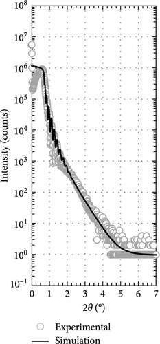
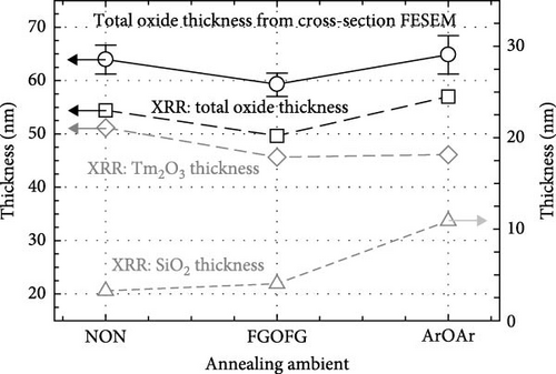
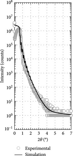
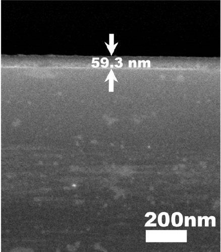
Two layers model on Si substrate was used in XRR fitting for determining the thickness of the Tm2O3 passivation layer and SiO2 interfacial layer by employing Bruker DIFFRAC Leptos (7.10.0.12) software (Figure 3). The thickness of the SiO2 interfacial layer formed after annealing process in different ambient as shown in Figure 4 has indicated that the annealing ambient comprising of nitrogen and/or hydrogen gases were more efficient in preventing the oxygen ions from interacting with the Si surface. Therefore, the sample annealed in ArOAr ambient attained the thickest SiO2 interfacial layer (10.893 nm), which agreed with previous postulation whereby the observation of the greatest oxygen at% (58.43 at%) for this passivation layer might be because of the generation of the thickest SiO2 interfacial layer. Besides, it was also disclosed that NON annealing was more effective in inhibiting the reaction between oxygen ions and Si (3.258 nm) than that of FGOFG annealing (4.026 nm). The reason for this observation might be linked to the larger ionic radius of nitrogen ions accumulating and forming the barrier layer at the Tm2O3/Si interface during NON annealing whereby more energy was needed for the oxygen ions to diffuse through this barrier layer and react with Si surface when compared with FGOFG annealing. When FGOFG ambient was employed, both hydrogen and nitrogen ions might be capable to diffuse to the interface. The smaller ionic radius of the hydrogen ion would enhance the susceptibility of oxygen ions to diffuse through the hydrogen ions and react with substrate. Another justification for the increased thickness of SiO2 after FGOFG annealing was due to the hydrogen ions having a greater tendency to create weaker bonding with Si dangling links when compared to the nitrogen ions. This has caused the oxygen ions to easily break the bonding between hydrogen ions and Si dangling bonds, resulting in the thickening of the SiO2 interfacial layer [39, 40]. Hence, the reaction between oxygen and Si surface was weaker for the samples annealed in NON and FGOFG ambient than that in ArOAr ambient as the oxygen vacancies sites available for the oxygen ions to hop to the interface was being reduced during annealing in NON and FGOFG ambient. In addition, the SiO2 interfacial layer of all annealed Tm2O3 passivation layers have increased from 0.217 nm for the as-deposited sample [35] to the range of 3.258–10.893 nm.
Details are in the caption following the image
XRR fitting patterns of Tm2O3 passivation layers subjected to (a) NON [35], (b) FGOFG, and (c) ArOAr annealing at 700°C. ArOAr, argon–oxygen–argon; FGOFG, forming gas–oxygen–forming gas; NON, nitrogen–oxygen–nitrogen; Tm2O3, thulium oxide; XRR, X-ray reflectivity.
Details are in the caption following the image
Total oxide thickness (cross-sectional FESEM images) as well as the total thickness, Tm2O3 layer thickness, and SiO2 interfacial layer thickness extracted from fitting XRR of Tm2O3 passivation layers experienced NON [35], FGOFG, and ArOAr annealing at 700°C. ArOAr, argon–oxygen–argon; FESEM, field-emission scanning electron microscopy; FGOFG, forming gas–oxygen–forming gas; NON, nitrogen–oxygen–nitrogen; SiO2, silicon oxide; Tm2O3, thulium oxide; XRR, X-ray reflectivity.

Besides, the effect of different annealing ambient on the thickness was evaluated by determining the thickness from XRR measurements. It was discovered that all of the annealed samples were undergoing densification process and demonstrated a thinner thickness ranging from 45.621 to 51.156 nm when compared with the as-deposited sample (61.687 nm) [35]. Among these investigated passivation layers, it was determined that NON ambient was less effective in densifying the Tm2O3 passivation layer, which might be associated with the occupancy of oxygen vacancies by nitrogen ions. With the nitrogen ions incorporated into Tm2O3 lattice, the adjacent oxygen ions in the Tm2O3 lattice were being released to achieve charge neutrality, whereby the densification of Tm2O3 passivation layer was restricted. Moreover, it was mentioned earlier that the larger radius nitrogen ions attached to the oxygen vacancies would hinder the oxygen diffusion. Thus, the densification of Tm2O3 passivation layer during annealing in NON ambient was hindered by the release of the adjacent oxygen and the incorporation of nitrogen. Despite the introduction of both hydrogen and nitrogen ions has taken place during annealing in an FGOFG ambient, the formation of the thinnest passivation layer has suggested that hydrogen ions with smaller ionic radius are more likely to bond with oxygen vacancies. This bonding increased the likelihood of oxygen ions diffusing through and filling these vacancies within the Tm2O3 lattice. Furthermore, the simultaneous occupancy of oxygen vacancies by both hydrogen and nitrogen ions during annealing in an FGOFG ambient did not cause the release of neighboring oxygen ions from the Tm2O3 lattice for charge neutrality. This is because the excess negative charges introduced by nitrogen ions are balanced by the positive charges generated when hydrogen ions were attached to the oxygen vacancies.

During postdeposition annealing in oxygen-deficient ambient, such as nitrogen, FG, and argon, oxygen will diffuse outward from the Tm2O3 lattice due to the difference in concentration gradient between the Tm2O3 layer and the annealing ambient. The outward diffusion of oxygen would result in the formation of doubly positively charged oxygen vacancies in the lattice since the two electrons carried by oxygen anion (O2−) that should occupy the lattice were missing. The two electrons were transferred to the neighboring Tm3+ cations, thus yielding a reduction of the oxidation state from Tm3+ to Tm2+. The processes were illustrated by the following half equations:
(3)
(4)
The N2 molecules from the nitrogen gas ambient would be adsorbed on the oxygen vacancies sites in the Tm2O3 lattice and dissociated into nitrogen anions (N3−). The N3− anions might substitute into the oxygen vacancies in the lattice since both N3− (143 pm) and O2− (140 pm) possessed similar ionic radius. Nonetheless, the substitution of N3− in one oxygen vacancy would trigger charge imbalance in the lattice, according to Equation (5) and thus inducing the formation of more oxygen vacancies in neighboring anion sites for charge neutrality:
(5)
However, when the Tm2O3 passivation layer was annealed in FG ambient consisting of 10% hydrogen and 90% nitrogen, the N2 and H2 molecules from the FG ambient would be adsorbed on the oxygen vacancies sites in the Tm2O3 lattice and dissociated into N3− and H+ ions. The relatively smaller radius of hydrogen ions was reactive, and the incorporation of the H+ ions with the lattice would form an electroneutral product, based upon the suggestion equation below:
(6)

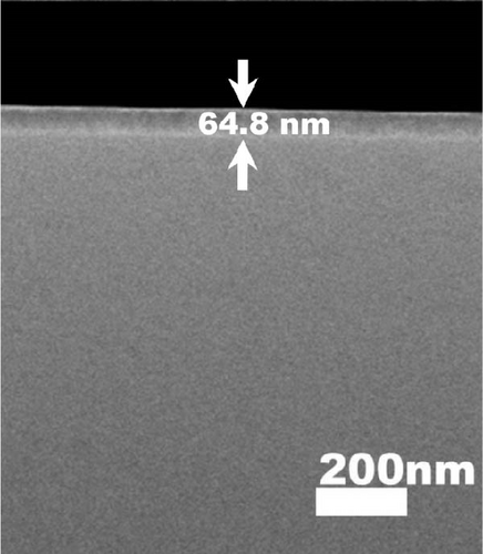
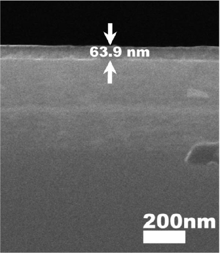
Therefore, the densification of Tm2O3 passivation layer during annealing in FGOFG ambient was less affected by the oxygen vacancies. Since the formation of SiO2 interfacial layer was more excessive in ArOAr ambient, the formation of more oxygen vacancies in the Tm2O3 passivation layer has reduced the densification process of Tm2O3 passivation layer, wherein a slightly thicker Tm2O3 passivation layer was acquired when compared with the sample annealed in FGOFG ambient. Overall, it was determined that the densification of the Tm2O3 passivation layer was hindered during annealing in NON because nitrogen ions attached to the oxygen vacancies have caused the formation of more oxygen vacancies. The cross-sectional images of the samples annealed in NON, FGOFG, and ArOAr ambient were shown in Figure 5, where in 10 measurements were taken using ImageJ software to determine total oxide thickness. Furthermore, the total thickness derived from XRR measurements and cross-sectional FESEM characterization were found to be comparable and exhibit a similar trend.
Details are in the caption following the image
Cross-sectional images (FESEM) of Tm2O3 passivation layers annealed at 700°C in different ambient of (a) NON [35], (b) FGOFG, and (c) ArOAr ambient. ArOAr, argon–oxygen–argon; FESEM, field-emission scanning electron microscopy; FGOFG, forming gas–oxygen–forming gas; NON, nitrogen–oxygen–nitrogen; Tm2O3, thulium oxide.
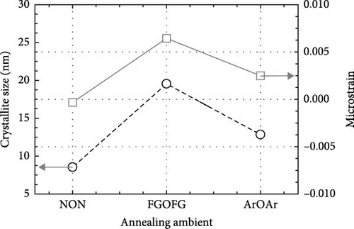
The effects of the NON, FGOFG, and ArOAr annealing on the microstrain (ε) and crystallize size (D) of the studied Tm2O3 passivation layers were also determined using the Williamson–Hall (W-H) approach expressed by the following equation [41]:
(7)
where the βi, θi, and λ denote integral breadth, diffraction angle, and X-ray wavelength. For the extracted ε and D of the investigated samples as shown in Figure 6, it was noticed that the NON annealing produced the smallest D for the Tm2O3 passivation layer due to both the restriction effect of the incorporated nitrogen ions and the induced extra oxygen vacancies. Although the FGOFG annealing has introduced both hydrogen and nitrogen ions into Tm2O3 lattice, the attainment of the largest D indicated that the largest D has been attained by this passivation layer as the release of oxygen ions was not encountered because these oxygen vacancies were occupied by both hydrogen and nitrogen ions, whereby the oxygen ions were more likely to replace the hydrogen ions during dwelling stage. An analysis comparing the Tm2O3 passivation layers annealed in FGOFG and ArOAr ambient has revealed that the Tm2O3 passivation layer treated with ArOAr annealing process has demonstrated a greater quantity of oxygen vacancies. The increase of oxygen vacancies has triggered oxygen ions to diffuse to the Tm2O3/Si interface, facilitating the reaction with Si to form SiO2 and a reduction in D value. The Tm2O3 passivation layer was induced with compressive ε when annealed in the NON ambient, while tensile ε was induced when annealed in the ArOAr and FGOFG ambients, leading to the acquisition of positive and negative ε values (Figure 6), respectively. The acquisition of compressive ε for the sample annealed in NON ambient can be ascribed to the introduction of nitrogen ions and the release of adjacent oxygen ions. Furthermore, the higher tensile ε was observed for the sample subjected to FGOFG annealing because of the simultaneous introduction of both hydrogen and nitrogen ions into the Tm2O3 lattice in which the adjacent oxygen ions abstained from being released have triggered the generation of additional tensile ε compared to the sample annealed in ArOAr ambient. This indicates that the concentration of oxygen vacancies has governed the acquisition of a lower tensile ε in the sample annealed in ArOAr ambient.
Details are in the caption following the image
Microstrain and crystallite size for Tm2O3 passivation layers experienced NON [35], FGOFG, and ArOAr annealing at 700°C. ArOAr, argon–oxygen–argon; FGOFG, forming gas–oxygen–forming gas; NON, nitrogen–oxygen–nitrogen; Tm2O3, thulium oxide.
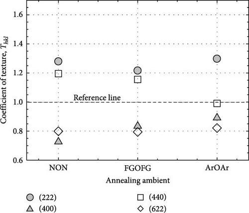
The evaluation on the growth orientation was conducted by extracting the coefficient of texture (Thkl), in accordance with the following equation [42]:
(8)
where n is the number of Tm2O3 reflection peaks and the Im(hkl) and Io(hkl) are the relative reflective intensities from (hkl) plane of the annealed and standard Tm2O3, respectively. It could be conveniently perceived from the calculated Thkl values (Figure 7) that the samples annealed in NON and FGOFG ambient demonstrated a T222 and T440 valuer greater than 1, suggesting that these samples were grown preferentially in (222) and (440) planes. Nonetheless, only T222 exceeding 1 was observed after ArOAr annealing, implying that Tm2O3 phase with (440) orientation was no longer predominating.
Details are in the caption following the image
Coefficient of texture (Thkl) for Tm2O3 passivation layers experienced NON [35], FGOFG, and ArOAr annealing at 700°C. ArOAr, argon–oxygen–argon; FGOFG, forming gas–oxygen–forming gas; NON, nitrogen–oxygen–nitrogen; Tm2O3, thulium oxide.

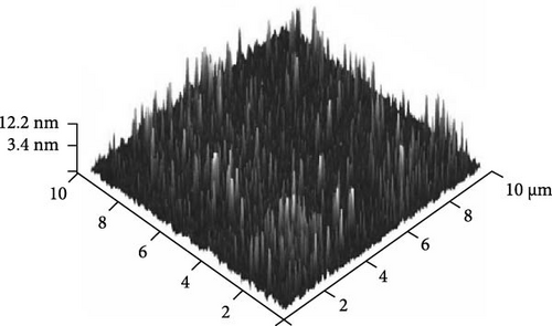
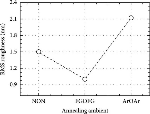
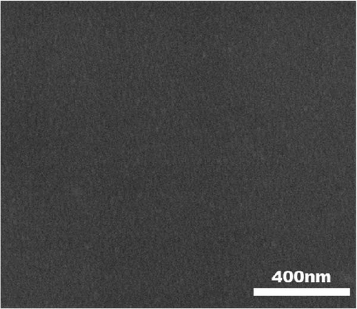
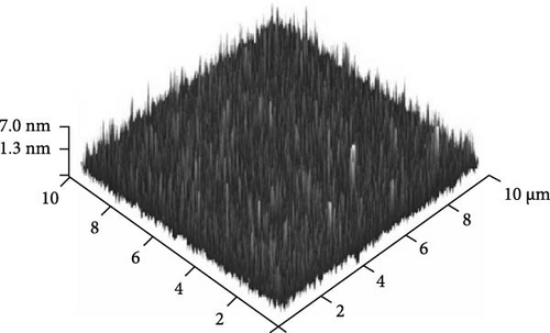
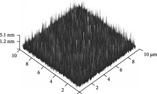
Furthermore, AFM was employed to evaluate the surface topographies of the Tm2O3 passivation layers during annealing in the NON, FGOFG, and ArOAr ambient, with a scanning area of 10 μm × 10 μm. The FGOFG annealing process, as illustrated in Figure 8, led to the uniform growth of protrusions with a comparable height across the surface, as well as the lowest RMS roughness (0.997 nm). The consistent densification throughout the Tm2O3 passivation layer during annealing in FGOFG ambient due to lesser release of the adjacent oxygen ions could explain this observation. By comparing with ArOAr annealing, the NON annealing would cause a weak densification on Tm2O3 passivation layer, while a protrusion with comparable height (Figure 8a) was formed due to the accumulation of the nitrogen ions at the Tm2O3/Si interface slowing down the reaction between oxygen ions and Si surface. Hence, the NON annealing resulted in a lower RMS roughness for the sample annealed in ArOAr ambient. Based on the fact of forming an excessively thick SiO2 interfacial layer after annealing in ArOAr ambient, uneven protrusions (Figure 8c) formed on this Tm2O3 passivation layer due to oxygen deficiency resulted in the highest RMS roughness (Figure 8d). Furthermore, surface morphologies of the Tm2O3 passivation layer annealing in NON, FGOFG, and ArOAr ambient were evaluated using FESEM, where no cracks and voids were formed on the smooth surface for all samples (Figure 9).
Details are in the caption following the image
Three-dimensional surface topographies for Tm2O3 passivation layers experienced (a) NON [35], (b) FGOFG, (c) ArOAr annealing at 700°C, and (d) root-mean-square (RMS) roughness of the investigated Tm2O3 passivation layers. ArOAr, argon–oxygen–argon; FGOFG, forming gas–oxygen–forming gas; NON, nitrogen–oxygen–nitrogen; RMS, root mean square; Tm2O3, thulium oxide.
Details are in the caption following the image
Surface FESEM image for Tm2O3 passivation layers experienced FGOFG, annealing at 700°C. FESEM, field-emission scanning electron microscopy; FGOFG, forming gas–oxygen–forming gas; Tm2O3, thulium oxide.
The Kubelka–Munk function was used to extract the direct (ED) and indirect (EID) bandgap of the investigated Tm2O3 passivation layers from the diffused reflectance spectra obtained using a UV-Vis spectrophotometer. This function can be represented by the following equation [43]:
(9)
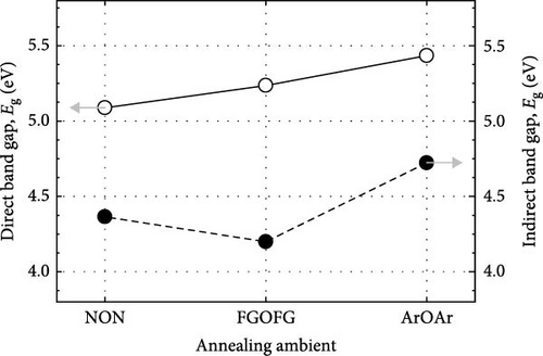
where R denotes diffuse reflectance and F (R) is the function of R used to extract the band gap. The curves of [F (R) × hv]2 and [F (R) × hv]1/2 with respect to hv was plotted (not shown) to determine direct Eg (ED) and indirect Eg (EID), respectively. Based on the literature, it was reported that the ED of bulk Tm2O3 was 5.400 eV [44], while the ED of Tm2O3 film deposited on Si substrate was 5.760 eV [20]. The ED and EID of the investigated Tm2O3 passivation layers were shown in Figure 10. It was revealed in this work that the ED of Tm2O3 passivation layer annealed in NON (5.088 eV) and FGOFG (5.236 eV) ambient was narrower than the reported ED for bulk Tm2O3 (5.400 eV) [44] and Tm2O3 film (5.760 eV) [20], which could be associated to the incorporation of nitrogen ions into the Tm2O3 lattice when FG and N2 were employed. Nonetheless, the Tm2O3 passivation layer annealed in ArOAr has attained a larger ED of 5.434 eV, which was comparable with the ED for bulk Tm2O3 (5.400 eV) [44]. In addition, it was noticed that NON annealing has attained the smallest ED because of the introduction of more nitrogen ions into the Tm2O3 lattice when compared with the sample annealed in FGOFG ambient. Therefore, the band gap of this sample was narrowed by a higher concentration of interband state caused by the nitrogen incorporation during NON annealing. Similar finding has been revealed by the nitrogen incorporated HfO2 passivation layer, whereby narrowing of band gap has taken placed as a result of the introduction of N2p states that have triggered occurrence of conduction band narrowing as well as valance band broadening [45]. Nevertheless, it was perceived that a smaller EID of 4.119 eV was acquired by the Tm2O3 passivation layer annealed in FGOFG ambient than NON ambient (EID = 4.364 eV), which could be linked to fact that the hydrogen ions from the FGOFG annealing ambient were induced into Tm2O3 lattice. This could be an indication that these induced hydrogen ions would give rise to a higher concentration of shallower energy level when compared with the nitrogen ions that would narrow the EID of the FGOFG annealed Tm2O3 passivation layer [46]. Since no foreign ions were introduced into the Tm2O3 passivation layer annealed in ArOAr ambient, the largest ED (5.434 eV) and EID (4.722 eV) have been obtained by this sample. Despite the samples annealed in FGOFG and NON ambient having narrower ED and EID values than the sample annealed in ArOAr ambient, the samples annealed in these ambient have nevertheless achieved ED and EID values that are large enough to offer a sufficient conduction and valence band offset with respect to the Si substrate.
Details are in the caption following the image
Direct and indirect band gap for Tm2O3 passivation layers experienced NON [35], FGOFG, and ArOAr annealing at 700°C. ArOAr, argon–oxygen–argon; FGOFG, forming gas–oxygen–forming gas; NON, nitrogen–oxygen–nitrogen; Tm2O3, thulium oxide.
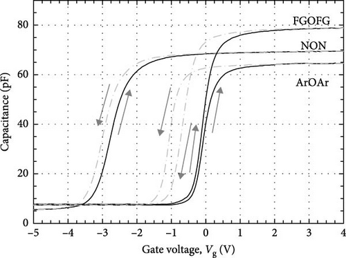
The C–V measured for the investigated Tm2O3 passivation layers subjected to NON, FGOFG, and ArOAr annealing was presented in Figure 11. It was worth noting that self-written code was employed in accordance with the theory described in the [47] for the fitting of the measured C–V curves with respect to ideal C–V curve. Based on Figure 11, the effect of different annealing ambient on the dielectric constant (k) values was calculated using the following equation [48]:
(10)
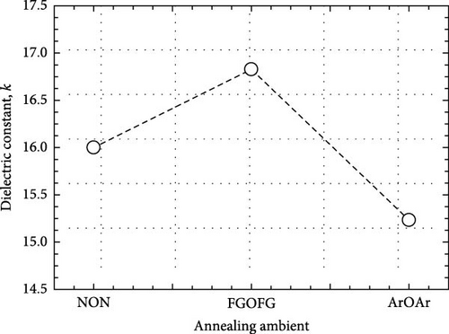
where ε0 is the permittivity of free space, Cox is the accumulation capacitance that measured at accumulation level, A is area of metal contact, and tox denote total oxide thickness of Tm2O3 passivation layers that measured from the cross-section FESEM characterization (Figure 4). Of these investigated samples, the lowest k value of 15.2 (Figure 12) was obtained for the sample annealed in an ArOAr ambient. This result further endorses the notion that the thick SiO2 interfacial layer (10.893 nm) generated in this sample was a result of the lack of hydrogen and nitrogen ions. Hence, the samples annealed in FGOFG and NON ambient obtained higher k values of 16.8 and 16.0, respectively, as the XRR results have indicated the formation of thinner SiO2 interfacial layer ranging from 3.258 to 4.026 nm. Although a thicker SiO2 interfacial layer (4.026 nm) was formed during annealing in FGOFG ambient, the attainment of a higher dielectric constant of 16.8 by this passivation layer when compared with that annealed in NON ambient (16.0) has denoted that the minute variation in the of SiO2 interfacial layer’s thickness was considered to have no substantial impact on the k value of the investigated samples. Furthermore, the lower k value observed in the sample annealed in NON ambient, compared to FGOFG ambient, might be due to the higher concentration of nitrogen ions and oxygen vacancies present in the samples annealed in NON ambient. Previous studies have shown that the presence of nitrogen ions in high-k materials and the formation of oxygen vacancies in high-k passivation layers have triggered an increment in dielectric [4951].
Details are in the caption following the image
C–V curves for Tm2O3 passivation layers experienced NON [35], FGOFG, and ArOAr annealing at 700°C. ArOAr, argon–oxygen–argon; FGOFG, forming gas–oxygen–forming gas; NON, nitrogen–oxygen–nitrogen; Tm2O3, thulium oxide.
Details are in the caption following the image
The k value of the Tm2O3 passivation layers annealed at 700°C in NON [35], FGOFG, and ArOAr ambient. ArOAr, argon–oxygen–argon; FGOFG, forming gas–oxygen–forming gas; NON, nitrogen–oxygen–nitrogen; Tm2O3, thulium oxide.
It was divulged that negative flatband voltage shift (ΔVFB) was measured from Tm2O3 passivation layers annealed in NON, FGOFG, and ArOAr ambient and presented as effective oxide charge (Qeff) determined by the following equation [52]:
(11)
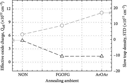
where q denotes electronic charge while the ΔVFB was calculated by comparing the shift in VFB between the ideal and measured C–V curves [47]. According to the determined Qeff shown in Figure 13, the sample annealed in NON ambient has attained the largest Qeff value (4.89 × 1012 cm−2) denoting the presence of the highest density of positive charged tarps in this sample. The obtained largest Qeff for the sample annealed in NON ambient agreed with earlier explanation, whereby a higher concentration of positively charged oxygen vacancies was formed contributing to the attainment of smallest D for this passivation layer. However, the sample annealed in FGOFG ambient achieved the lowest Qeff value of 1.32 × 1012 cm−2, indicating that the occupation of oxygen vacancies by hydrogen and nitrogen ions has impeded the released of adjacent oxygen ions. Furthermore, the likelihood of inward diffusing oxygen ions to disrupt the hydrogen ion interaction with oxygen vacancies was increased. Consequently, a greater number of oxygen ions might be diffused and occupied the oxygen vacancies in the sample that was annealed in the FGOFG ambient. A marginal increment in Qeff value (1.34 × 1012 cm−2) was gained by the sample annealed in ArOAr ambient when compared with FGOFG ambient suggesting that the absence of hydrogen and nitrogen ions has triggered a higher concentration of oxygen ions to diffuse to the interface contributing to the generation of thickest SiO2 interfacial layer (10.893 nm). Hence, by comparing with FGOFG annealing, the ArOAr annealing induced more oxygen vacancies in the Tm2O3 passivation layer.
Details are in the caption following the image
Effective oxide charge (Qeff) and slow trap density (STD) of the Tm2O3 passivation layers annealed at 700°C in NON [35], FGOFG, and ArOAr ambient. ArOAr, argon–oxygen–argon; FGOFG, forming gas–oxygen–forming gas; NON, nitrogen–oxygen–nitrogen; Tm2O3, thulium oxide.
The slow trap density (STD) of the investigated samples was determined from the bidirectional C–V curves using the following equation [53]:
(12)
where ΔV denote the difference in flat-band voltage between forward and reverse bias. It can be conveniently observed from Figure 13 that the sample annealed in ArOAr ambient demonstrates the highest STD due to the presence of the abundant of oxygen vacancies and the absence of nitrogen and/or hydrogen ions in passivating the Si dangling bonds, wherein these positively charged oxygen vacancies as well as Si dangling bonds located near to the interface would be able to capture and release the injected electrons when forward and reverse biases were applied. It was noticed that the sample annealed in FGOFG ambient has resulted in a higher STD than that in NON ambient because of the attachment of hydrogen ions to the Si dangling bonds. When positive bias was applied to the sample annealed in FGOFG ambient, the injected electrons might have gained sufficient energy to break the bonding of hydrogen ions to the Si dangling bonds. Therefore, these Si dangling bonds were capturing the subsequent injected electrons when further increment in forward bias was applied. Then during the reverse bias, the electrons would de-trap from the Si dangling bonds and demonstrated a higher STD for Tm2O3 passivation layer annealed in FGOFG ambient than NON ambient. Since the employment of NON annealing has stimulated the accumulation of more nitrogen ions at the Tm2O3/Si interface, the injected electrons during forward bias would not be attracted to these negatively charged nitrogen ions, and thus, the probability of electrons to be trapped would be lower, thus resulting in the lowest STD value.
The interface quality with regard to interface trap density (Dit) of the Tm2O3 passivation layers annealed in NON, FGOFG, and ArOAr ambient was determined using the following equation [54]:
(13)
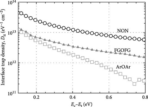
where Φs represents the responding Si surface potential for a given voltage while the ΔVg represents voltage difference between the gate voltage acquired experimentally (Vg) and ideally from the ideal C–V curve (Vg(ideal)) [47]. As shown in Figure 14, the Tm2O3 passivation layer after NON annealing demonstrated the highest Dit as a result of the highest content of nitrogen ions on the Si/Tm2O3 interface. This observation was consistent with the degrading effect of nitrogen annealing on interface quality of Al2O3 passivation layer where the Dit was increased from ~1.5 × 1013 to ~3.0 × 1013 cm–2 after annealing in nitrogen [55]. On the other hand, the nitrogen barrier layer might prevent oxygen ions from reacting with the Si surface, thereby contributing to a higher Dit for the samples annealed in NON and FGOFG ambient. Hence, it was observed that an improvement in Dit was achieved after ArOAr annealing, wherein the thickest SiO2 interfacial layer would annihilate the interface traps and improve the interface quality. The sample experiencing FGOFG annealing demonstrated a lower Dit than NON ambient, which might be attributed to the accumulation of lesser nitrogen ions at the interface as well as the possibility of oxygen ions to break the attachment of hydrogen ions with Si dangling bonds. As a result, the reaction between these oxygen ions and Si would be stimulated to form interfacial layer and reduce the Dit. Although the sample annealed in FGOFG ambient has a higher Dit ranging from 1.4 to 7.0 × 1012 eV–1cm–2 than the sample annealed in ArOAr ambient (0.2 to 5.5 × 1012 eV–1cm–2), the range of Dit values obtained by the sample annealed in FGOFG ambient was comparable to the reported Dit values for HfO2 (3.0 × 1012 eV–1cm–2) [56], Y2O3 (ranging from 2.0 to 8.0 × 1012 eV–1cm–2) [57], and ZrO2 (ranging from 3.0 to 7.0 × 1012 eV–1cm–2) [58] passivation layers deposited on Si substrate.
Details are in the caption following the image
Interface trap density (Dit) for the Tm2O3 passivation layers annealed at 700°C in NON [35], FGOFG, and ArOAr ambient as a function of EcEt plot. ArOAr, argon–oxygen–argon; FGOFG, forming gas–oxygen–forming gas; NON, nitrogen–oxygen–nitrogen; Tm2O3, thulium oxide.
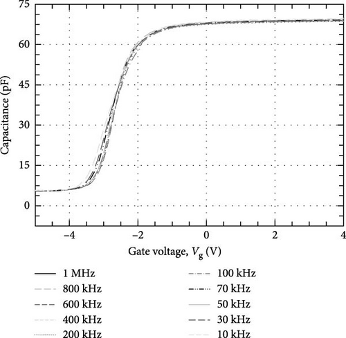
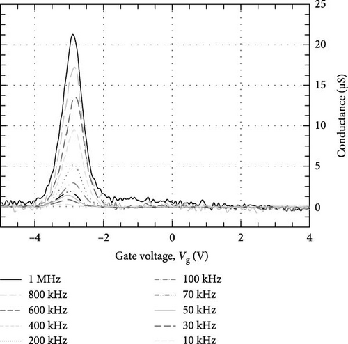
Besides, based on the CV and GV characteristics of the investigated samples that were measured at different frequencies (10–1000 kHz), the investigation on the interface quality was also conducted using Hill–Coleman and high–low frequency methods. To eliminate the effect of the series resistance in the measuring circuit, the obtained CV and GV curves were corrected using the method presented in [47, 59]. Based on the CcV and GcV results as shown in Figure 15, the Dit was calculated using the Hill–Coleman method [59]:
(14)
where Gc,max is the maximum conductance in GcV result, Cc,max denotes the corrected capacitance at the voltage corresponding to Gc,max, and Cox represent the corrected capacitance of the corresponding passivation layers that calculated from Gm,acc and Cm,acc using the method presented in [47, 59].
Details are in the caption following the image
The typical (a) corrected capacitance–voltage (CcV) as well as (b) corrected conductance–voltage (GcV) curves for the Tm2O3 passivation layers annealed in NON ambient at 700°C. NON, nitrogen–oxygen–nitrogen; Tm2O3, thulium oxide.
Details are in the caption following the image
The typical (a) corrected capacitance–voltage (CcV) as well as (b) corrected conductance–voltage (GcV) curves for the Tm2O3 passivation layers annealed in NON ambient at 700°C. NON, nitrogen–oxygen–nitrogen; Tm2O3, thulium oxide.

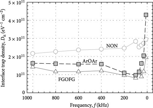
Figure 16 depicts the calculated Dit (Hill–Coleman mothed) for the investigated samples. Overall, it was determined that both Hill–Coleman and Terman’s methods have revealed similar trend for the sample annealed in NON ambient, wherein this passivation layer has attained the highest Dit values. Nonetheless, a discrepancy between the trend obtained from Hill–Coleman and Terman’s methods for both Tm2O3 passivation layers annealed in ArOAr as well as FGOFG ambient has revealed that the acquisition of a greater Dit (Hill–Coleman method) value by the sample annealed in ArOAr ambient might be associated with the presence of the greatest STD for this passivation layer. The attainment of the lowest Dit (Hill–Coleman method) value for the Tm2O3 passivation layer experiencing FGOFG annealing has further suggested the hydrogen in FG was more effective in eliminating the interface related defects. It was also revealed in other research work, whereby the FG annealing for Al2O3 passivation layer has resulted in an interface state density of ~5 × 1012 cm−2 which is lower than nitrogen annealing (~3 × 1013 cm−2) [55].
Details are in the caption following the image
Interface trap density (Dit) of the Tm2O3 passivation layers annealed at 700°C in NON, FGOFG, and ArOAr ambient calculated by Hill–Coleman mothed. ArOAr, argon–oxygen–argon; FGOFG, forming gas–oxygen–forming gas; NON, nitrogen–oxygen–nitrogen; Tm2O3, thulium oxide.
In addition, based on the corrected CV results, the Dit were also calculated using high–low frequency C–V method [60]:
(15)
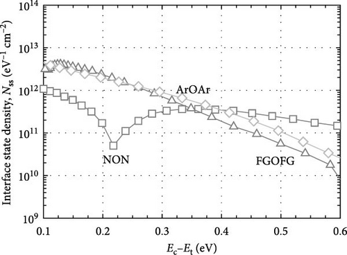
where CLF is the corrected capacitance calculated from the capacitance measured at 10 kHz and CHF is corrected capacitance calculated from the capacitance measured at 1 MHz. Figure 17 displays the calculated Dit from the high–low frequency C–V method for the investigated passivation layers, wherein the EcEt was derive from the surface potential [61] which was determined using Berglund’s integral as described in the references [62]. From Figure 17, it was deduced that Tm2O3 passivation layers annealed in FGOFG and ArOAr ambient have demonstrated a higher Dit near to the conduction band edge and decreased as the energy level moved away from the conduction band edge. This observation could be associated to the ability of oxygen ions to passivate the traps located further away from the conduction band edge during annealing in FGOFG and ArOAr ambient. Besides, the availability of hydrogen ions during annealing in FGOFG ambient has resulted in the acquisition of the lowest Dit at Ec–Et level larger than 0.38 eV in which these hydrogen ions would be able to diffuse to a higher energy level to passivate these traps. Nonetheless, an increment in Dit was noticed when the EcEt was enhanced beyond 0.22 eV, which could be linked to the formation of nitrogen barrier layer that have impeded the oxygen ions from repairing the interface related traps. It has been discovered that the sample annealed in NON ambient has exhibited the lowest Dit at EcEt values below 0.22 eV. This indicates that oxygen ions have acquired sufficient energy to surpass the nitrogen barrier layer and rectify the interface-related traps within this specific range of EcEt.
Details are in the caption following the image
Interface trap density (Dit) of Tm2O3 passivation layers annealed at 700°C in NON, FGOFG, and ArOAr ambient calculated using high-low frequency method. ArOAr, argon–oxygen–argon; FGOFG, forming gas–oxygen–forming gas; NON, nitrogen–oxygen–nitrogen; Tm2O3, thulium oxide.

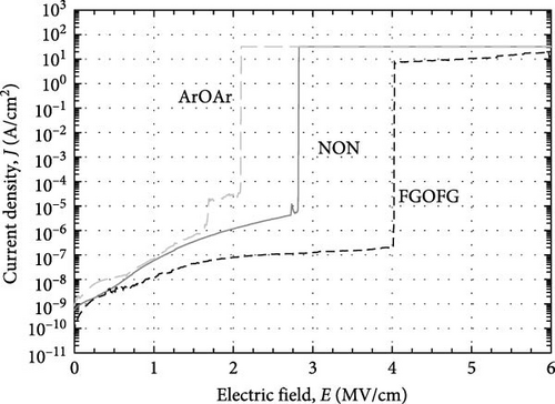
The leakage current density–electric field (JE) characteristics of the investigated Tm2O3 passivation layers was presented in Figure 18. Among the investigated passivation layers, the sample which underwent FGOFG annealing showed the lowest J and the highest EB (4.03 MV/cm). This can be attributed to its highest k value, the lowest Qeff, the lowest Dit calculated using the Hill–Coleman method, and lowest Dit at Ec–Et level greater than 0.38 eV calculated using the high–low frequency method. Although the sample experiencing NON annealing ambient has attained the lowest STD as well as the lowest Dit at Ec–Et smaller than 0.22 eV (calculated using high-low frequency method), the attainment of a lower EB (2.83 MV/cm) by this sample when compared with the sample annealed in FGOFG ambient has suggested that the influence of these two parameters toward the EB could be less significant. It was postulated that for the acquisition of the highest Qeff, the highest Dit calculated from both Terman and Hill–Coleman methods by the sample annealed in NON ambient has also contributed to the deterioration in J–E characteristic. Nonetheless, it was observed that the Tm2O3 passivation layer experiencing ArOAr annealing ambient has demonstrated a soft breakdown at 1.69 MV/cm, which might be a sign of the breakdown of the thicker SiO2 interfacial layer (10.893 nm). The observation of a hard breakdown at 2.10 MV/cm by the sample annealed in ArOAr ambient has suggested that the formation of a higher concentration of oxygen vacancies has triggered degradation in the passivating properties of this Tm2O3 passivation layer.
Details are in the caption following the image
Leakage current density–electric field (JE) characteristics of the Tm2O3 passivation layers annealed at 700°C in NON, FGOFG, and ArOAr ambient. ArOAr, argon–oxygen–argon; FGOFG, forming gas–oxygen–forming gas; NON, nitrogen–oxygen–nitrogen; Tm2O3, thulium oxide.

4. Conclusion

The effects of NON, FGOFG, and ArOAr annealing ambient on the passivating characteristics of the Tm2O3 passivation layer have been comprehensively evaluated. It was concluded that annealing in NON ambient was the most effective ambient in impeding the formation of SiO2 interfacial layer as the XRR measurement has revealed the formation of thinnest SiO2 interfacial layer of 3.258 nm. In addition, the EDX measurement revealed that the highest at% of nitrogen (5.59%) was acquired during annealing in an ambient of NON. This finding further confirmed that a larger number of nitrogen ions have been accumulated at the interface between the Tm2O3 passivation layer and the Si substrate, effectively reducing the formation of the SiO2 interfacial layer. However, the incorporated nitrogen ions would narrow the band gap by inducing more interband state when compare with FGOFG and ArOAr annealing, where the highest direct band gap (ED = 5.434 eV) and indirect band gap (EID = 4.722 eV) were attained from the Tm2O3 passivation layer annealed in ArOAr ambient. Significantly, the FGOFG annealing would prompt the Tm2O3 passivation layer gain the highest k value (16.8) owing to its capacity to prevent the formation of both the SiO2 interfacial layer and oxygen vacancies. With the both beneficial effects of hydrogen and nitrogen, the FGOFG annealing demonstrated the lowest concentration of effective oxide charge (Qeff) of 1.32 × 1012 cm−2 and the lowest interface trap density (Dit), which have been proved by Terman, Hill–Coleman, and high–low frequency methods. Additionally, the excellent interface quality together with an acceptable thickness of SiO2 interfacial layer contributed to a lower leakage current density and a higher breakdown electric felid (4.03 MV/cm) for the Tm2O3 passivation layer annealed in FGOFG ambient.

Conflicts of Interest

The authors declare no conflicts of interest.

Funding

The authors would like to acknowledge the financial support from the Ministry of Higher Education Malaysia for Fundamental Research Grant Scheme (FRGS) with Project Code FRGS/1/2023/STG05/USM/02/8.

Acknowledgments

The authors would like to acknowledge the financial support from the Ministry of Higher Education Malaysia for Fundamental Research Grant Scheme (FRGS) with Project Code FRGS/1/2023/STG05/USM/02/8.

    Data Availability Statement

    The raw/processed data required to reproduce these findings cannot be shared at this time as the data also form part of an ongoing study.

      The full text of this article hosted at iucr.org is unavailable due to technical difficulties.