ANFIS-Controlled Boost and Bidirectional Buck-Boost DC-DC Converters for Solar PV, Fuel Cell, and BESS-Based Microgrid Application
Abstract
DC-DC converters are essential for integrating distributed energy resources into microgrid (MG) systems. These converters are designed to incorporate intermittent renewable energy sources such as solar photovoltaic (PV) panels, fuel cells (FCs), and battery energy storage systems (BESSs) into the grid. However, conventional DC-DC converters have limitations including lower efficiency, voltage ripple, insufficient voltage regulation, and compatibility issues. This article presents boost and bidirectional buck-boost converters for direct current microgrid (DCMG) applications, employing an adaptive neuro-fuzzy inference system (ANFIS) for control. These proposed converter configurations adeptly manage wide input voltage fluctuations from intermittent sources, consistently supplying power to the DC bus at 500 V and 120 V for boost and buck operations, respectively, with an efficiency of 98.8%. The output voltage result shows that the ANFIS-based boost converter has 10% overshoot as compared to 41% and 50% overshoot in proportional integral (PI) and fuzzy logic controller (FLC), respectively. In both buck and boost modes, the converters’ voltage gain is influenced by duty ratio adjustments only, not sensitive to dynamic input voltage and flexible manipulation of the output voltage for BESS charging. Moreover, the designed converters accommodate load variations within the MG. To assess the converters’ ability to regulate output voltage effectively, PI, FLC, and ANFIS controllers are implemented and compared. And the ANFIS controller demonstrates superior performance, offering faster response times and enhanced stability. Evaluations are conducted through simulations in the MATLAB/Simulink environment.
1. Introduction
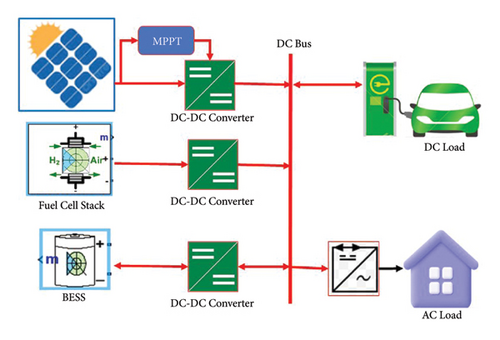
An MG is a self-contained power system that combines distributed energy resources (DERs) and different controllers within a defined location. It operates as a single controllable unit, able to function in either grid-connected mode or independently in islanded mode. An MG can be DC, AC, or hybrid sourced to accommodate both AC and DC loads. DCMG is the most proposed architectures due to inherently experiencing lower energy losses compared to AC systems, leading to more efficient power utilization, and also DC microgrids (DCMGs) has reduced costs, improved power quality, and are suitable to integrate DERs [1–3]. For instance, as depicted in Figure 1, DERs such as solar PV, FC stacks, and battery energy storage systems (BESSs) are linked to a shared DC node through relevant DC-DC converters. The solar PV system employs its own maximum power point tracker (MPPT) and connects to a DC-DC boost converter. Similarly, the FC stack plant utilizes a DC-DC boost converter to ensure a consistent output voltage at the common DC bus [4]. The BESS is interfaced with a bidirectional buck-boost converter, facilitating the charging of the battery from the DC bus during surplus power from the MG. During the buck mode operation of the buck-boost converter, the common DC bus voltage needs to be decreased to charge the BESS to its nominal voltage [5]. Significantly, the BESS plays a crucial role in mitigating peak demands, thereby reducing operational costs and enhancing system reliability [6].
1.1. Motivation
Amid the growing global energy crisis, microgrids are seen as a crucial strategy for tackling energy issues. This research study focuses on improving the smooth operation of DC microgrids by utilizing an efficient DC-DC boost converter for solar PV and FC plants, along with a bidirectional buck-boost converter for integrating BESS into the microgrid. This paper evaluates the efficiency and speed of these converters by employing an ANFIS controller, which minimizes voltage fluctuations and maintains the output voltage at the desired level.
1.2. Related Works
Numerous DC-DC converters have been developed and studied to tackle the previously mentioned challenges. Various topologies and controllers, from classical to intelligent approaches, are explored in this context. For instance, Liu et al. [2] employed supertwisting high-order sliding-mode control to reduce converter output voltage overshoot in a photovoltaic-based DC microgrid (MG). This method resulted in a 33% reduction in system overshoot, significantly enhancing response speed, with stability confirmed via Lyapunov theory control [7].
In another study, Ullah et al. [8] introduced a bidirectional buck-boost converter regulated by a sliding-mode controller (SMC) to ensure system stability despite variations in the energy storage device (ESD) voltage. Lai et al. [9] implemented a two-phase, interleaved, bidirectional DC-DC converter topology for electric vehicles and DC microgrids. The results indicated that this design effectively minimized output ripple, achieving efficiencies of 98.4% in buck mode and 97.7% in boost mode for a small-scale prototype MG model.
A fractional-order PID controller approximation was proposed for voltage regulation in a buck-boost converter in [10]. The results demonstrated that signal stability remained consistent for low-voltage applications using operational amplifiers, validated with commercial parameters. In another study [11], a bidirectional DC-DC converter controlled through a PI controller processed and triggered the converter switch, resulting in stable output voltage with some input current ripples under variable PV-sourced MG. Yfoulis et al. [12] employed a PID-controlled boost and buck-boost DC-DC converter in a DCMG under uncertain mixed load conditions. The output voltage was governed by a PID as the primary controller and model predictive control (MPC) based on specialized current and power estimators [13].
AI methods have proven effective in managing nonlinear systems, such as those found in DERs modeling and interfacing converters [14]. Unlike classical techniques, AI approaches excel in extracting maximum power from PV arrays, optimizing hydrogen fuels, and managing BESS for improved performance. These methods are efficient with nonlinear systems, offering speed, flexibility, and reliability [15]. Among soft-computing AI techniques, artificial neural networks (ANNs), fuzzy logic controllers (FLCs), and ANFIS are used for DER generation control and converter design, ensuring fast response and stable output in intermittently sourced MGs and interfacing DC-DC converters. Rouzbehi et al. [16] proposed a data-driven voltage control strategy for DC-DC converters, utilizing a local model network (LMN) to identify a dynamic model for the converter across its operating regime. This strategy processes the generated control signal (duty ratio, D) to enable efficient operation in buck and boost modes for MG applications. Liu et al. [17–20] introduced a droop control method for multiple DC-DC converters, demonstrating effective power sharing in an MG by balancing the load. Koundi et al. [21] applied closed-loop Lyapunov stability control to a fuel cell-fed interleaved buck-boost converter, ensuring the DC voltage tracks and its desired value despite load uncertainties, and facilitating adequate current sharing between the fuel cell and IBBC. However, this study did not address response speed or input and output ripples [22].
The reviewed literature emphasizes that the effectiveness of a microgrid (MG) control system relies heavily on the accuracy and reliability of both the MG model and its controller. Traditional control methods, such as the PI controller, require precise mathematical models of the MG to manage voltage and frequency [23]. Conversely, AI-based control strategies, such as ANN and FLC methods, operate without needing exact mathematical models and can adeptly handle the system’s nonlinear dynamics [24]. Fuzzy-based dynamic control of DCMG has proposed in [25] to improve the power management control of renewable energy-integrated MG. ANFIS-PID- and FA-PSO-based DCMG has proposed by considering electric vehicle charging ecosystems for assuring stability of DC microgrids [26].
Regarding high-power DC-DC boost and bidirectional buck-boost converter interleaving techniques, some existing models lack DER self-interleaving or AI-based control. For instance, Aditama et al. [27] proposed a multilevel modular buck-boost converter without considering MPPT for interleaving or powerful controllers. Lv et al. [28] used three control loops for a high-voltage-gain boost converter without interleaving, resulting in high sensitivity of the output voltage to input variations [29, 30]. Some models neither used the interleaving technique nor AI-based control. This study explores the design and modeling of high-power DC-DC converters using an ANFIS controller, integrating solar PV arrays, FC stacks, and BESS to create a robust DCMG configuration [31, 32]. The proposed model incorporates the interleaving technique for DC-DC converters and employs an ANFIS controller for DERs, such as in PV array MPPT, FC closed-loop control, and BESS management as the primary control. Modifications to the DC-DC converters include using high-power IGBT devices for high-frequency switching and fast response, and replacing the RC circuit in parallel with the output capacitor [33, 34]. FLC-based MPPT has been implemented to respond instantly to changes in PV array resources and environmental conditions, remaining unaffected by circuit parameter changes [35]. An FLC/ANFIS/ANN-based MPPT technique for a buck-boost converter is presented by Guerra et al. [15], considering ambient conditions (solar irradiance and temperature) as input variables. Results show that the ANN outperforms in tracking speed, accuracy, and reducing oscillation around the maximum power point (MPP) [36]. Khan et al. [37] introduced a voltage control strategy for the DC-DC boost converter using an ANN-based approach, where MPC acts as an expert providing data to train the ANN [38]. The ANN control strategy outperforms the PI controller across various loading conditions, achieving about 97% accuracy during model training [4]. This design assumes that the values of the inductor and capacitor in both the boost and bidirectional buck-boost converters remain constant and do not deviate from their nominal values.
However, the preceding discussion highlights a significant gap in the use of ANFIS techniques for designing controllers for DC-DC converters to address issues such as voltage ripple, inefficiency, inadequate voltage regulation, and compatibility problems. The proposed ANFIS-controlled DC-DC converters, powered by intermittently sourced DERs, effectively manage ripple current and single-stage control issues while maintaining a constant DC bus voltage despite wide-ranging input voltage and load demand variations. Simulation tests confirm that the implementation of the ANFIS controller on interleaved DC-DC converters is highly efficient for high-power converter applications in MGs.
1.3. Major Contributions
- (i)
It introduces high-voltage-gain DC-DC boost and bidirectional buck-boost converters using ANFIS-based control to obtain high efficiency and fast response by considering nonideal dynamic input voltage from distributed energy resources (DERs), and at the same time, ANFIS is also used to model solar PV, FC, and BESS systems to reduce the influence of uncertainties.
- (ii)
It demonstrates how the proposed converters are capable of accommodating a wide range of input voltages from variable DERs and applying different loads, yielding nearly constant output voltages at the common DC bus.
- (iii)
While traditional droop control effectively distributes power between the BESS and DC, it tends to result in higher voltage deviations, consequently hastening BESS capacity degradation. In this paper, the BESS incorporates its own ANFIS controller for managing state of charge (SoC) during charging and discharging operations, ensuring a consistent nominal voltage for the bidirectional buck-boost converter input.
1.4. Paper Organization
The reminder of this work is organized as follows: Section 2 presents MG component modeling with detail description. Section 3 discusses the DC-DC converter controller ANFIS with detail explanation and definition to apply on the proposed system. Section 4 discusses the design of DC-DC high-power boost and bidirectional buck-boost converters for MG applications. Section 5 summarizes the simulation results and discussion. Finally, in Section 6, conclusion is drawn along with suggested future works.
2. System Component Modeling
2.1. Mathematical Model of Solar PV Module
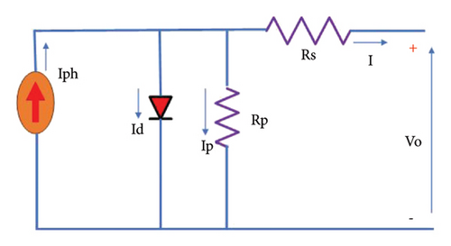
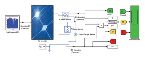
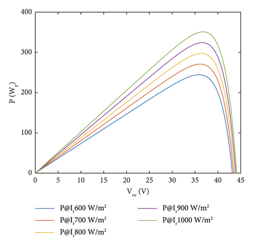
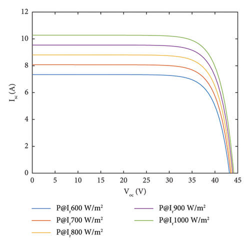
In this paper, a standard PV module has been simulated to evaluate the characteristics of the module based on the influencing parameters such as irradiance and temperature. Figure 3 shows the Simulink module of a standard PV module of 360 Wp rated power to demonstrate characteristic curves based on intermittent resources. Figure 4 shows the P-V and I-V characteristic curves to show the relationship between the open circuit voltage, short circuit current, and output power of the module by considering the irradiance and temperature. The PV system parameter of the selected module specification is shown in Table 1.
| Parameter | Quantity |
|---|---|
| Solar irradiance (test irradiance) | 1000 W/m2 |
| Maximum power (Pmax) | 350 Wp |
| Voltage at Pmax (Vmp) | 37.0 V |
| Current at Pmax (Imp) | 9.71 A |
| Open circuit voltage (Voc) | 43.2 V |
| Short circuit current (Isc) | 10.1 A |
| Maximum system voltage | 100 V DC |
| Cell efficiency | 20.06% |
| Number of by-pass diodes | 6 |
| Maximum series fuse | 15 A |
| Nominal operating cell temperature | 47 ± 2°C |
2.2. Fuel Cell Modeling
The FC and BESS parameters are illustrated in Table 2 that are used in the modeling of the unit FC stack and BESS. Figure 5 shows the ANFIS-controlled MATLAB/Simulink model of a standard 45 V, 6 kW fuel cell stack where the hydrogen flow rate is controlled by the ANFIS to optimize the accumulated hydrogen gas in the hydrogen tank. The V-I and P-I characteristic curve of the given FC stack is shown in Figure 6 that shows the relationship of the stack voltage and power versus the current. As the V-I curve shows, as the stack current increases, the voltage will decrease, and the P-I curve depicts that the output power of the FC stack increases as the stack current or the the hydrogen utilization rate increases. Hence, it is compulsory to optimize and control the flow rate of the gases in the stack.
| Parameter | Quantity |
|---|---|
| Stack power | 6 kW |
| Stack voltage | 45 V |
| Nominal hydrogen utilization | 99.56% |
| Nominal oxidant utilization | 59.3% |
| Hydrogen fuel flow rate | 50.06 lpm |
| Air (oxygen) flow rate | 300 lpm |
| System temperature | 338 Kelvin |
| Fuel supply pressure | 1.5 bar |
| Air supply pressure | 1.0 bar |
| Battery type | Lithium ion |
| Nominal voltage | 187 V |
| Rated capacity | 30 A |
| Initial state of charge | 80% |
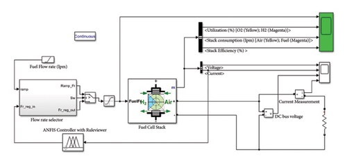
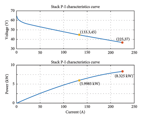
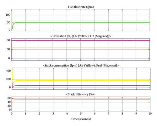
Figure 7 depicts the FC stack parametric values which show the FC flow rate in liters/minute (lpm) resulted around 55 lpm and the utilization of oxygen (labeled yellow) and hydrogen (labeled red) are 60% and 100%, respectively. And the stack consumption of air (labeled green) and fuel consumption are 180 lpm and 50 lpm, respectively, and as shown in the Figure 7, the FC stack efficiency is around 56%.
2.3. BESS and SoC Modeling
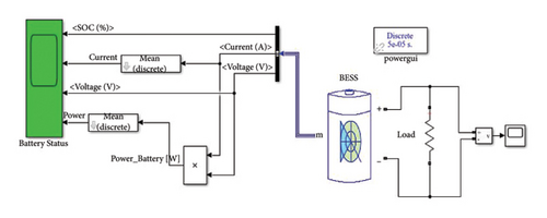
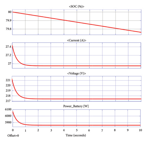
Figure 8 shows the MATLAB/Simulink model of a unit BESS system with measurement features to see the BESS state-of-charge (SoC), current, voltage and power during the simulation. And Figure 9 shows the SoC which represents the energy stored in the battery expressed as percentage between 0% and 100%, current which is dependent on the load connected, system voltage, and output power of the BESS. In this case, the SoC is depleted from 80% to 79.96% for 10 seconds.
3. Proposed Real-Time Controller: ANFIS
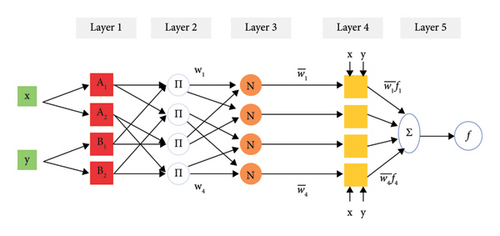
ANFIS attracts a worldwide attention due to its robust control and improves the dynamic behavior of the system. The ANFIS controller, which combines the benefits of ANNs and FLCs, is now regarded as one of the most effective tools for system identification, pattern recognition, and building precise models of systems [43]. Figure 10 shows the architecture of the ANFIS model with five layers. At the first layer, inputs (errors and error changes) will be sent to the second layer without processing. The second layer, each membership function is represented in a fuzzy cluster [44]. At the third layer, minimization of input sets will be applied at each node. The fourth layer is a defuzzification stage which extracts the fuzzy sets of each node. At the fifth layer, output of each node at the fourth layer will be accumulated for the final value of the ANFIS controller. ANFIS uses Sugeno-type inference system that provides a structured method for generating if-then rules by formalizing the input-output relationship in a systematic manner. As Figure 10 illustrates ANFIS two inputs and one output structure where x and y are crisp inputs, and f is the crisp output. Referring to Figure 10, two rules are articulated for the first-order Sugeno fuzzy inference system as follows [45–47]: rule 1: if x is A1 and y is B1, then f1 = p1x + q1y + r1, rule 2: if x is A2 and y is B2, then f2 = p2x + q2y + r2, where x and y denote inputs, Ai and Bi are fuzzy variables, fi represents outputs within fuzzy sets, and pi, qi, and ri are design parameters established through the training process of the ANFIS system. Figure 10 illustrates the architecture of ANFIS. In this depiction, a fixed node is denoted by a circle, while an adaptive node is represented by a square. ANFIS features a five-layer structure, with nodes in each layer serving comparable functions. Detailed explanations for each layer are given as follows.
3.1. Layer 1
3.2. Layer 2
These are the so-called firing strength of the rules.
3.3. Layer 3
Outputs of this layer are called normalized firing strengths.
3.4. Layer 4
3.5. Layer 5
4. Design of DC-DC Boost and Buck-Boost Converters
4.1. Mathematical of Buck and Boost Converters
4.2. DC-DC Boost Converter Model
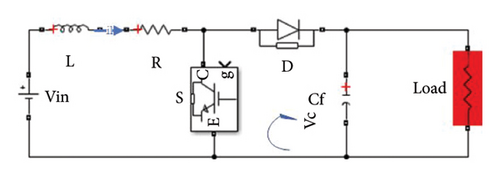
DC-DC boost converter for microgrid application is similar to a conventional boost converter; it increases the DC voltage from its input (sourced from renewable energy sources, batteries, or other microgrid elements) to the microgrid’s DC bus. The proposed converter as shown in Figure 13 is designed to accommodate wide range of input voltages from different renewable DC voltage sourced such as solar PV, FC, and BESS with high transient response during the generation and demand changes and high-power efficiency. The booster is controlled through the application of adaptive PI controller, fuzzy logic controller, and ANFIS to compare and choose the suitable controller with fast response and high accuracy. The designed converter desired output voltage is 500 V and the input sources are designed for 300 V with variable and intermittent nature in the solar PV and FC stacks which has to be further optimized through electronic maximum power point tracker (MPPT).

The solar array voltage is set to 300 V by embedding the MPPT internally, and the FC stack is also designed for 300 V by increasing the number of cells in the stack and optimizing the hydrogen and air flow rate. Then, the DC-DC boost converter is implemented to step-up the 300 V to a constant 500 V DC for the DC subgrid.
4.3. DC-DC Buck-Boost Converter Model
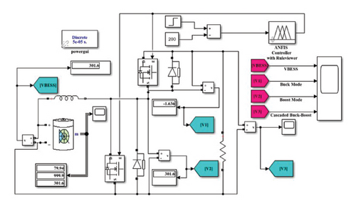
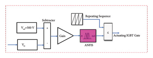
Unlike a buck converter (step-down) or a boost converter (step-up), a buck-boost converter can both increase and decrease the DC voltage, depending on the operating mode. This allows for flexible power flow management within the MG. The designed buck-boost converter is implemented on BESS-based DC subgrid to charge the battery from the DC bus through the buck converter side when there is surplus energy from the renewable energy sources and to utilize the BESS power when there is a power deficiency to shave the peak demand of the MG trough the boost side of the converter so that the overall operating cost will be minimized. IGBT switch, S1, is used to optimize/actuating the buck mode operation of the converter where the input voltage is VBESS and the output voltage is V1 through PI, FLC, and ANFIS controllers for comparison. And S2 is triggered by the proposed controllers to optimize the boost side converter by keeping the input voltage, VBESS, and the output voltage is V2. By summing both converter output voltages, the converter can be a cascaded converter which can act as a bidirectional buck-boost converter and a cascaded converter that can synchronize the main system DC bus at a constant voltage of 500 V of the DCMG as shown in Figure 12. The proposed ANFIS closed-loop controller was used to optimize and actuate the IGBT PWM signal for voltage regulation in both buck and boost modes of operation by keeping the DC bus voltage 500 V as a reference.
Table 3 illustrates the boost converter design parameters that is assumed and calculated based on trial and error for the desired DC bus voltage output in the DCMG application. By having the aforementioned parameters in the boost converter, the buck and cascaded converters are also formulated from the boost converter design parameters by amending the values by assumption and trial and error method until the target point reaches the desired voltage values of each converters. Figure 14 highlights the subsystem diagram of the controllers.
| No. | Parameter | Designed value |
|---|---|---|
| 1 | Input voltage | 300 V |
| 2 | Output voltage | 500 V |
| 3 | Input current | 252 A |
| 4 | Output current | 123.6 A |
| 5 | Load resistance | 200 Ω |
| 6 | System test load | 61.5 kW |
| 7 | Duty cycle | 0.5 p.u. |
| 8 | Switching frequency | 250 kHz |
| 9 | Inductor | 76.8∗10−6 H |
| 10 | Capacitor | 400∗10−6 F |


5. Simulation Results and Discussion
The proposed soft-computing algorithms and methodology are executed in the MATLAB R2022b academic version Simulink environment using a machine with processor speed of 2.4 GHz Intel Core i7 and 16 GB RAM.
Figure 15 shows the output voltages of PI/FLC/ANFIS-controlled DC-DC boost converter for the DCMG application by accommodating intermittent voltage sourced renewable energy resources such as solar PV, FC stacks, and BESS in the MG. As the result depicts the ANFIS-based control is more accurate and faster than PI and FLC. Since the ANFIS has the advantages of both the ANN and FLC, it is clear that the efficiency of the converter is higher than the adaptive PI and FLC. The output voltage result shows that the ANFIS-based boost converter has 10% overshoot as compared to 41% and 50% overshoot in PI and FLC, respectively. And the settling time in ANFIS is 0.01 seconds which is fastest as compared to 0.015 seconds and 0.05 seconds in FLC and PI controllers, respectively.
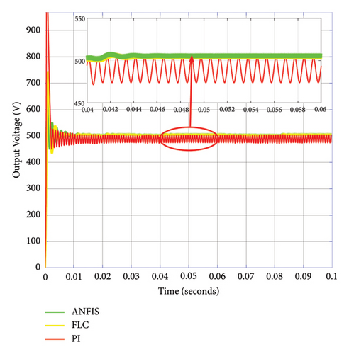
Figure 16 shows the ANFIS-based boost converter parameter simulation results. As the scope depicts, the input PV array, FC, and BESS voltage is set to 300 V by implementing an implicit ANFIS controller for each plants such as MPPT booster in the PV array, fuel flow rate optimization in the FC stack, and state-of-charge (SoC) controller in the BESS. Then, by using the converter ANFIS controller, the voltage is further stepped-up to 500 V which is assumed as the output voltage of the DC bus. Hence, the ANFIS controller effectively handles the regulation task in the boost converter for the proposed MG application. Furthermore, as the scope shows the input current in the PV array and FC was 238.6 A, but the boost converter effectively reduced the input current to 121.5 A in the output port. The variation in the buffering DC link capacitor voltage is measured at 1.14%. This fluctuation is minimized on the capacitor side, ensuring that the output voltage remains stable. With a permissible limit of 5%, the proposed ANFIS has effectively reduced the DC link voltage variation to a significantly lower value within this limit.
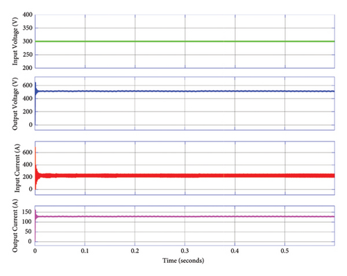
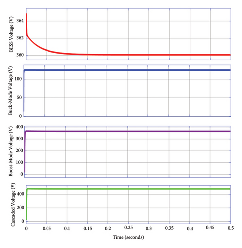
Figure 17 depicts the bidirectional buck-boost converter simulation result. When the bidirectional buck-boost converter is applied on the BESS for the charging and discharging applications, the BESS voltage is around 360 V under the initial SoC of 80% then under the buck mode operation, the output buck voltage is 120 V which can charge the BESS effectively with the help of embedded charge controller. The booster side has stepped-up the input BESS voltage to 360 V, and by cascading the two converters, the DC bus will receive 500 V from the BESS through the bidirectional buck-boost converter.
The operation of buck and boost converters are actuating by the pulse width modulation (PWM) through the ANFIS controller. In the simulation, it has also observed that the duty ratio during the ANFIS operation to ON and OFF the IGBT switch has been stepped-up or stepped-down with a certain voltage gain from the pulse that triggered the gate of the IGBT. The measurement showed that the mean value is around 0.48 p.u. and ranges from 0 to 1. For bidirectional buck-boost converter, the duty ration for buck mode and boost mode operations is different which is directly proportional to the voltage gains in each mode of operation.
Table 4 illustrates the voltage gain sensitivity in buck and boost modes of operation. As the load resistance/demand in the MG increases, the output voltage of the converter is consistent in both modes of operations. Even if there is a slight voltage drop as the load change is getting bigger, the converters are effective to handle reasonable load changes in the MG for practical applications since the simulation is set up with the real renewable energy-sourced voltage supplies. Hence, it can be concluded that the voltage gain is not sensitive to the load change in both converter operations.
| No. | Load resistance (Ω) | Boost mode output voltage (V) | Buck mode output voltage (V) |
|---|---|---|---|
| 1 | 50 | 500.5 | 119.9 |
| 2 | 100 | 500.09 | 119.8 |
| 3 | 150 | 500.05 | 119.6 |
| 4 | 200 | 500.01 | 120.0 |
| 5 | 250 | 500.00 | 120.05 |
| 6 | 300 | 500.00 | 120.06 |
| 7 | 350 | 500.0 | 120.09 |
| 8 | 400 | 499.96 | 120.09 |
Table 5 depicts the voltage gain sensitivity in buck and boost operation modes by varying the input voltage. As the input voltage is from the intermittent energy sources such as solar PV, FC stacks, wind power, and energy storage systems (ESSs), the output voltage of these sources are variable. The designed buck and boost converters are receiving a variable input voltage from 200 V − 320 V, then regulates the output voltage to a consistent and constant voltage of 500 V and 120 V for boost and buck converters, respectively. As the input voltage ranges from 200 V to 320 V and the output voltages are then regulated by the ANFIS controller to a constant voltage of 500 V and 120 V for the converter. Hence, both converters have 98.8% efficiency at the optimum duty ratio and can accommodate variable input voltages from dynamic energy sources. The ANFIS is working on the pulse width modulation operation where the actuating signal is a square wave that controls the IGBT gate. Consequently, the duty cycle can be adjusted within the range of 0 to 1 p.u., as depicted in Figure 18.
| No. | Input voltage (V) | Boost mode output voltage (V) | Buck mode output voltage (V) |
|---|---|---|---|
| 1 | 200 | 499.15 | 119.2 |
| 2 | 220 | 499.69 | 119.9 |
| 3 | 250 | 499.98 | 119.99 |
| 4 | 270 | 500.00 | 120.00 |
| 5 | 290 | 500.00 | 120.00 |
| 6 | 300 | 500.00 | 120.00 |
| 7 | 310 | 500.04 | 120.02 |
| 8 | 320 | 500.06 | 120.03 |
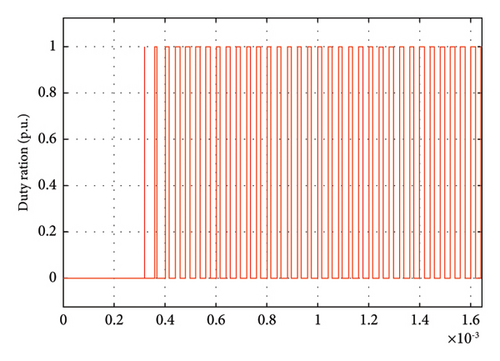
Table 6 demonstrates the output voltage at different duty cycle values ranging from 5% to 50%. As the duty ratio increases, the buck and boost converters output voltage increases. Therefore, the duty ratio is the key factor to vary the output voltage of the converters.
| No. | Duty ratio (%) | Boost mode output voltage (V) | Buck mode output voltage (V) |
|---|---|---|---|
| 1 | 5 | 25.95 | 5.24 |
| 2 | 10 | 45.23 | 7.45 |
| 3 | 15 | 72.49 | 7.99 |
| 4 | 20 | 94.56 | 8.78 |
| 5 | 25 | 121.97 | 9.92 |
| 6 | 30 | 150.29 | 1025 |
| 7 | 35 | 182.54 | 12.96 |
| 8 | 40 | 205.74 | 25.20 |
| 9 | 45 | 235.10 | 70.67 |
| 10 | 50 | 493.30 | 89.90 |
Since the proposed circuit is a simplified form of the conventional model of the boost converter, diodes and other passive elements are reduced and replaced with a controllable IGBT and maintained using the ANFIS controller that tries to reduce the error and always follow the desired DC voltage. Hence, the designed converter efficiency is almost 99.5% as calculated from Table 5.
6. Conclusion
This article presents DC-DC boost and bidirectional buck-boost converter configurations designed for DC microgrid applications. It compares the performance of these converters using PI, FLC, and ANFIS controllers. The ANFIS controller demonstrated the highest efficiency, approximately 98.8%, for the proposed converter designs. Compared to traditional boost and buck-boost converters, the ANFIS-controlled converter models effectively handle variable input voltages from intermittent renewable energy sources such as solar PV, fuel cell stacks, wind power, and BESS. Simulations with real-time PV arrays, fuel cell stacks, and BESS showed the converters achieving voltage outputs of 500 V and 120 V at the boost and buck converter ports, respectively. Despite significant input voltage variations and load fluctuations, both converters maintained stable output voltages after a 10% overshoot lasting only 0.05 seconds.
Furthermore, this study suggests that future work could involve validating the performance of the proposed converters in a nonideal DER-sourced laboratory, aiming for a scalable design and enabling seamless expansion to support multiple ports for EV charging infrastructure or higher power requirements in hybrid microgrids.
Conflicts of Interest
The authors declare that they have no conflicts of interest.
Acknowledgments
This work was supported by the Pan African University Institute for Basic Sciences, Technology and Innovation (PAUSTI).
Open Research
Data Availability
The data used to support the findings of this study are available from the corresponding author on request.


