Mechanical Strain-Modulated Multifunctional Pr-Doped BaTiO3 Thin Film for Luminescence Sensing and Piezoelectric Energy-Harvesting Applications
Abstract
Piezoelectric materials with tunable photoluminescence have gained widespread attention for their application in optical communications and optoelectronic sensing devices. This has provided new opportunities to explore the possibility of developing flexible piezoelectric devices with both piezoelectricity and photoluminescence for multifunctional applications. In this study, we prepared a crystalline Pr-doped perovskite BaTiO3 (BPTO) film on a flexible mica substrate using the radio-frequency (RF) sputtering technique. The photoluminescence intensity remarkably increased by about 210% when external mechanical stress was applied to the film. This remarkable increase in photoluminescence is attributed to lattice distortion and a decrease in crystal symmetry. The BPTO film also exhibited reversible and high-endurance behavior even after 103 fatigue bending cycles. Moreover, the BPTO film was utilized as a piezoelectric nanogenerator device, which demonstrated a maximum output voltage of about 2.68 V when external stress was applied through palm tapping. The nanogenerator device yielded an instantaneous output power of 1.80 μW with an external load resistance of 0.8 MΩ. These versatile and robust properties of the BPTO film demonstrate its potential for future development of lead-free self-powered optoelectronic sensing applications, such as artificial intelligence and biomedical devices.
1. Introduction
In recent years, rapid technological advancements have prompted the development of multifunctional electronic devices that prioritize transparency, portability, and flexibility [1, 2, 3]. Flexibility is important when developing wearable electronics, displays, electronic skin, and implantable devices [4, 5]. Piezoelectric materials with distinct electrical, mechanical, thermal, and optical characteristics, such as piezoelectric perovskite thin films, have emerged as a potential option for the development of multifunctional flexible electronics that can be integrated with piezoelectric, electrical, and photonic features for diverse applications [6, 7, 8]. Moreover, piezoelectric thin films are preferred because they exhibit better flexibility and piezoelectric performance than brittle ceramics, which reduce compatibility and device durability. Lead-based perovskites, such as Pb1−xZrxTiO3 (PZT), Pb (Mg1/3Nb2/3)O3-PbTiO3, and Na0.5Bi0.5TiO3, have been explored for various applications because of their excellent piezoelectric properties. However, owing to the hazardous nature of lead, finding a suitable lead-free alternative is becoming increasingly necessary. There is considerable interest in the development of piezoelectric materials for multifunctional applications, and BaTiO3 (BTO) has emerged as a promising alternative material for various photonic applications, including information processing and flat display technologies [9]. BTO with a tetragonal structure (space group: P4mm) is known for its remarkable piezoelectric constant of 191 pc/N, low leakage current, high spontaneous polarization, low coercive field, biocompatibility, and high optical transparency, all of which make it ideal for integration into optoelectronic devices [10, 11]. Various previous studies on BTO have mainly focused on enhancing its luminescence or piezoelectric properties [12, 13]. Additionally, studies on light-emitting devices have used rare-earth doping because it produces effective luminescent activator ions for various applications such as optical waveguides, long-distance communications, displays, and bioimaging [14, 15, 16]. Among the rare earths, praseodymium (Pr) ions have proven to be effective luminescent activator ions with red emission in the wavelength range of 600–650 nm [17, 18]. Although BTO is a highly effective piezoelectric material, there have been limited investigations into its characteristics and the implications of modulating its luminescence using strain.
As the demand for wearable and flexible electronics grows, developing flexible devices becomes increasingly crucial. Nevertheless, their multifunctionality can be further enhanced by employing various methods that involve the integration of additional functionalities such as photoexcitation and mechanical stimuli. However, it is noteworthy that there has not been much emphasis on using these functionalities to create integrated devices with improved piezoelectric and luminescent sensing. Moreover, the piezoelectric properties of these materials can be improved through rare-earth doping to enhance their piezoelectric applications [19]. Recently, the use of an external electric field has been considered as a mode of tuning photoluminescence (PL) in rare-earth-doped ferroelectric and antiferroelectric materials [20, 21]. Zhang et al. [22] used an electric field to induce an antiferroelectric–ferroelectric phase transition in Er-doped Pb0.96La0.04Zr0.9Ti0.1O3 ceramics to achieve 30% enhancement in reversible PL. Rare-earth ions usually create a lattice distortion of the host lattice, consequently altering the crystal symmetry around the host lattice, which in turn affects the PL intensity [23]. Thus, using external stress to modify the crystal structure of inorganic materials could be a new method of PL modulation for sensing applications. Therefore, the simultaneous use of flexible devices for PL and piezoelectricity coupled with the ability to respond to external stimuli such as electric fields, pressure, and temperature could lead to the development of multifunctional piezoluminescent devices for various sensing photonic devices.
Researchers have conducted extensive investigations to facilitate the integration of perovskite thin films into flexible electronics [24, 25]. Various techniques, including sol–gel processing, molecular beam epitaxy, pulsed laser deposition, chemical vapor deposition, and atomic layer deposition, have been successfully employed to synthesize high-quality BTO films [26, 27, 28, 29, 30]. Among these, radio-frequency (RF) sputtering has garnered significant attention because of its cost-effectiveness, low to high-temperature deposition, large-scale deposition, and uniform high-quality film production [31, 32]. Materials must have good mechanical and bendability properties for real-world flexible electronic applications. Composite film materials with an elastomer matrix possess remarkable material piezoelectric characteristics. However, they typically have substantial thicknesses often in the range of hundreds of microns, making them challenging to downsize and integrate into microsensing systems. These limitations can be mitigated by adopting mica substrates for perovskites using various deposition techniques [33, 34, 35]. Mica substrates have a remarkably high melting point of ~1,150 K, making them ideal for high-temperature deposition [36]. Moreover, their unique layered structures allow for convenient exfoliation facilitated by the influence of van der Waals force governing the interlayer interactions while maintaining good mechanical strength, transmittance, and flexibility even at a thickness below 100 μm [37, 38]. Zou et al. [39] reported a 1 μm-thick perovskite PZT mica-based nanogenerator that yields an output voltage of 0.8–2.0 V and a current of 150–250 nA.
In this work, we studied a multifunctional lead-free flexible Pr-doped BTO (BPTO) thin film deposited on a mica substrate using the RF sputtering technique. The study also focused on luminescence modulation via a nondestructive approach with external mechanical strain applied through bending at different curvatures. The PL intensity was found to increase as the applied strain on the flexible substrate increased. Furthermore, we also studied the potential of this flexible film for nanogenerator applications by applying various forms of pressure on it. This study could pave the way for the development and design of next-generation multifunctional optoelectronic sensing devices.
2. Experimental and Material Characterization
2.1. Density Functional Theory Simulation Details
Computational structural analysis and density of states analysis were performed on the pristine and doped BTO using the CASTEP code with the density functional theory (DFT) principle based on the ultrasoft pseudopotential plane wave technique [40]. The local density approximation (LDA) + U approach was performed on a 2 × 2 × 3 supercell structure of 60 atoms, and a cut-off energy of 630 eV was used for the electron-transfer potential [41]. A Monkhorst–Pack grid of 2 × 2 × 2 k-points with a mixing scheme of Pulay was used for Brillouin zone integration. The relaxation convergence energy tolerance for ions and electrons was set to 1 × 10⁻⁵ eV, the self-consistent field tolerance was set to 1 × 10⁻⁶ eV/atom, and the Broyden–Fletcher–Goldfarb–Shanno technique was employed for the optimization. Ultrasoft potential modeling of electron–ion interactions was conducted, and valence electron configurations of Ba 5s25p66s2, Ti 3s23p63d24s2, O 2s22p4, and Pr 5s25p66s24f3 were used for Ba, Ti, O, and Pr, respectively, in order to describe the interactions between the valence electrons and ionic cores.
2.2. Film and Device Preparation
Initially, the sputtering target was prepared by mixing BaCO3 (99.9% purity, Sigma–Aldrich), TiO2 (99.9% purity, Sigma–Aldrich), and Pr2O3 (99.9% purity, Sigma–Aldrich) in ethanol for 12 hr. The well-mixed powder was dried at 60°C for 24 hr. Subsequently, the powder was annealed at 1,200°C for 10 hr. The sputtering target was obtained by pressing the powder in a Cu mold. BTO and BPTO films were prepared using RF magnetron sputtering, with a high purity (99.99%) target. Mica and silicon substrates were ultrasonically cleaned with acetone, methanol, deionized water, and isopropanol successively for 15 min to remove native oxide from them. Afterward, they were dried using nitrogen gas before use. The base pressure inside the chamber was pumped to 2.0 × 10⁻⁶ Torr before the deposition. The films were deposited at room temperature, and sputtering was performed for 1 hr in an Ar atmosphere kept at 20 sccm. The distance between the sample and the target was around 10 cm, and the sample holder was rotated at 25 rpm to ensure film uniformity during deposition. For the nanogenerator device, a Sn:In2O3 bottom electrode was deposited on the mica substrate via RF sputtering for 25 min, and Al was used as the top electrode.
2.3. Material Characterization
The crystal structure of the prepared films was characterized using high-resolution X-ray diffraction (HR-XRD; SmartLab Rigaku). The composition elemental distribution and chemical bonding states were investigated using X-ray photoelectron spectroscopy (XPS; Thermo Scientific Inc.) with an Al Kα μ-focused monochromator (1,486.6 eV). The acquired XPS spectrum was calibrated using the C 1s peak. The Jasco V-750 UV–visible spectrophotometer was used to acquire the transmittance spectra in the wavelength range of 300–900 nm. The Tauc plot obtained from the UV–visible spectra was used to determine the optical bandgap. The PL spectrum was collected using a LabRam ARAMIS spectrometer (Horiba Jovin Yvon) within the UV–visible range of 325 nm, and a He–Cd laser source was employed at room temperature to excite the sample. Generally, near-edge X-ray absorption fine structure (NEXAFS) is an effective tool for probing electronic structures; it employs soft X-rays to excite electrons from the core level to partially filled and empty states. The NEXAFS measurement of the oxygen K-edge and the analysis of the secondary cut-off and valence band region for the electronic band structure were performed using the Pohang Accelerator Laboratory (PAL) 4D beam line. The secondary cut-off of all the samples with respect to the Au reference was obtained after applying a negative voltage of −50 V. The local piezoelectric properties of BTO and BPTO deposited on a Pt substrate were determined using piezoelectric force microscopy (PFM; Nanoscope V Multimode 8, Bruker) and a Pt/Ir-coated Si cantilever with a conductive tip. The out-of-plane effective d33 was measured over a local surface area of 3 × 3 μm2 using a lock-in amplifier at 40 kHz and the drive voltage of 10 V was determined by measuring the displacement. The open-circuit voltage of the piezoelectric nanogenerator was measured using a nanovoltage meter (Keithley, DMM6500 USA). The output voltage of the nanogenerator at various load resistances (10 kΩ –6 MΩ) was determined using a voltage meter, and the respective current and power were calculated based on the output voltage and load resistance.
3. Results and Discussion
3.1. Film Analysis
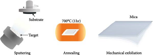
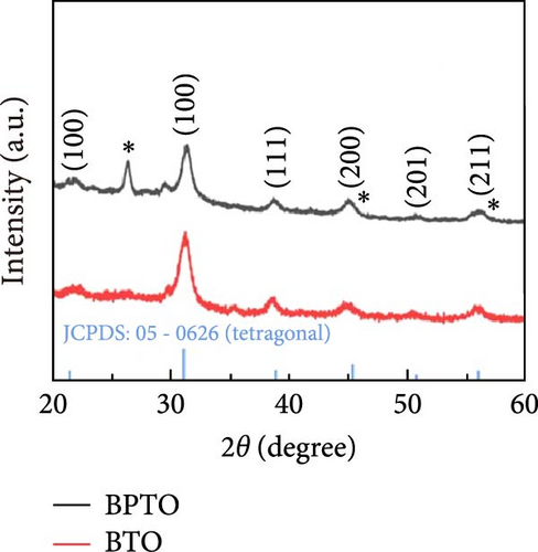
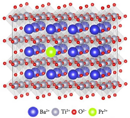
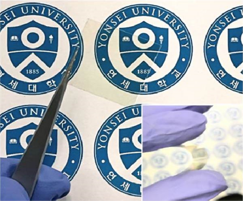
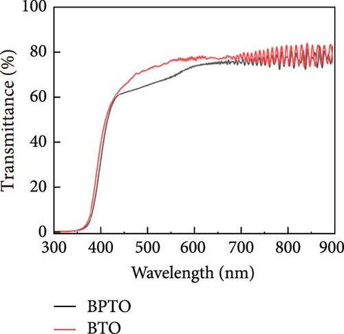
Figure 1(a) illustrates the fabrication of the thin film using a deposition process that involves RF sputtering, followed by an annealing process at 700°C, and epitaxial exfoliation of a mica substrate after crystallization. The crystalline quality of the BTO and BPTO film deposited on mica substrates was examined using HR-XRD, as shown in Figure 1(b). Both films exhibited a crystalline nature, with all the diffraction peaks corresponding to the tetragonal structure of BTO (JCPDS: 05-0626) belonging to space group P4mm [42]. The XRD patterns of the BTO and BPTO films deposited on Si substrates displayed a typical perovskite structure without any secondary phases, as depicted in Figure S1. The slight shift in the (110) peak toward a higher angle may be attributed to the replacement of Ba2+ ions with large radii (1.61 Å) by Pr3+ ions with small radii (0.99 Å), which results in a reduction in interplanar crystal spacing and lattice shrinkage [43]. Figure 1(c) shows the BPTO film with an ABO3 perovskite structure, where Pr3+ substitutes Ba2+ (A-site), Ti4+ is the B-site, and O2− is the O-site. As shown in Figure 1(d), the exfoliated thick mica sputtered with the BPTO film exhibited high flexibility and transparency, enabling the pattern and logo to be visible through the sample. Figure 1(e) illustrates the optical transmittance of the samples deposited on mica substrates. All the samples exhibited good transmittance of over 70% in the visible range. Figure S2(a) depicts the FE-SEM images of the BPTO film which shows a uniform growth of fine grains. The presence of Pr dopants has been confirmed from the EDX spectrum, as shown in Figure S2(b). The cross-sectional FE-SEM images of BPTO deposited on the mica substrate reveal a thickness of about 128.5 nm in Figure S3.
3.2. XPS Analysis
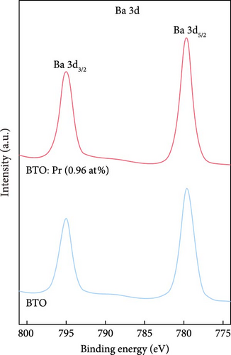
XPS analysis was conducted to investigate the surface chemical composition and valence state of the prepared samples. The Ba 3d peak can be resolved into two components (Ba 3d5/2 at 779.28 eV and Ba 3d3/2 at 794.53 eV) corresponding to barium in BTO, as depicted in Figure 2(a). The Ti 2p3/2 and Ti 2p1/2 peaks at binding energies of 457.52 and 463.03 eV, respectively, correspond to tetravalent titanium (Ti4+), while the two additional shoulder peaks at low binding energies of 461.12 and 456.17 eV correspond to Ti3+ in as illustrated in the deconvoluted Ti 2p spectrum in Figure 2(b) [44, 45].
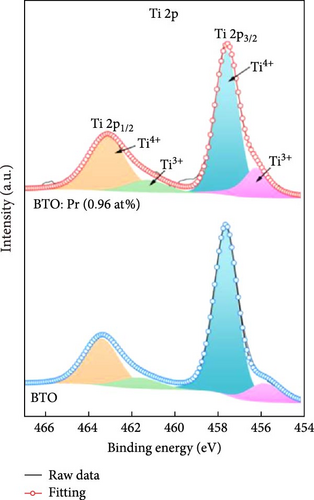
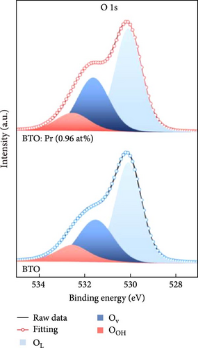
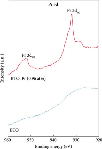
As shown in Figure 2(c), the O 1s peak is deconvoluted and composed of three peaks located at 530.06, 531.59, and 532.47 eV, which correspond to lattice oxygen bonded to the perovskite BTO structure (OL), oxygen vacancy (OV), and surface-adsorbed oxygen atoms (OOH), respectively [46, 47]. When some of the Ti4+ in BTO transformed to Ti3+, the increase in the number of oxygen vacancies was compensated by the higher Ti3+ content in BPTO relative to that in pristine BTO. The high Ti3+ content further confirms that the Pr ion replaces the Ba site to form free electrons [48]. Based on previous XPS studies, the presence of Ti3+ and OV states suggests the existence of defect sites on the surface [47]. XPS confirmed the presence of Pr3+ ions in BPTO at a concentration of ~0.96 at.%. Moreover, as shown in Figure 2(d), the Pr 3d spectra indicate the presence of two peaks corresponding to spin–orbit Pr 3d3/2 and Pr 3d5/2 around 951.54 and 931.76 eV, respectively. These two prominent peaks are attributed to the trivalent Pr3+ valence state [49, 50].
3.3. Electronic Structure and Gap Study
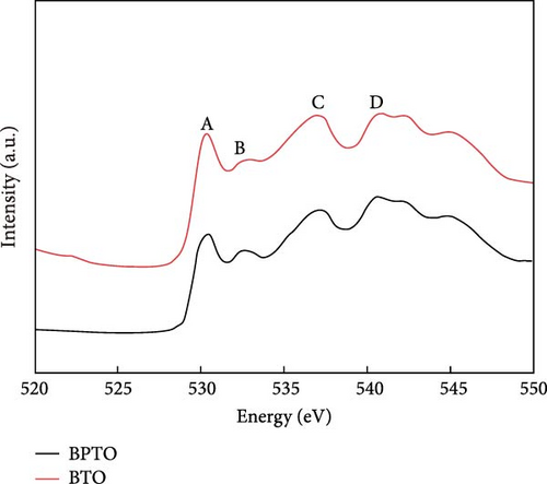
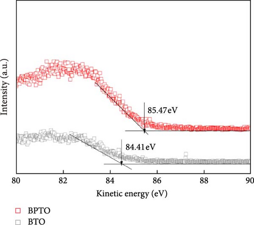
NEXAFS measurements were conducted to examine the electronic and chemical surroundings of O ions in the pristine BTO and BPTO samples. The O K-edge NEXAFS spectra in Figure 3(a) display four main peaks. Peak A near 530 eV corresponds to the excitation of the hybrid states of O 2p and Ti 3d t2g and eg orbitals, while peak B is mainly attributed to the O 2p hybridized with Ti 3d and Ba 5d [51, 52, 53]. The lowering of the peak B intensity in the doped sample is due to a decrease in the bonding of O 2p–Ba 5d/Pr 4d, which leads to an increase in the distortion and recombination of TiO6 octahedrons. When rare-earth Pr3+ ions are introduced, the O 2p–Ti 3d coupling reduces because Pr has a lower electronegativity than Ti, which facilitates electronic charge transfer from Pr to Ti after doping [54]. The broad peak C corresponds to the hybrid states of O 2p and transition metal Ti 4sp, as well as the hybrid states of O 2p and Ba 3d. The transition from the O 1s orbital to the hybrid orbital between the O 2p and Ti 4sp levels led to the broadening of peak C. The peak D around 540 eV corresponds to the transition of O 1s to O 2p–Ba 4f-derived states that are hybridized with Ti and Pr high-energy states [53, 55]. Figure 3(b) shows the valence band spectra of the pristine BTO and BPTO samples. The valence band edges were determined by employing a linear extrapolation method to identify the maximum negative slope near the edge and the minimum horizontal baseline. The resulting valence offsets of BTO and BPTO were measured to be 84.41 and 85.47 eV, respectively. The decrease in bandgap was observed in BPTO, as shown in Figure S4. The UV–vis absorption spectra of BTO and BPTO have been shown in Figure S5. More UV absorption and a red shift in the absorption edge have been observed in the BPTO samples which could be attributed to the decrease in bandgap.
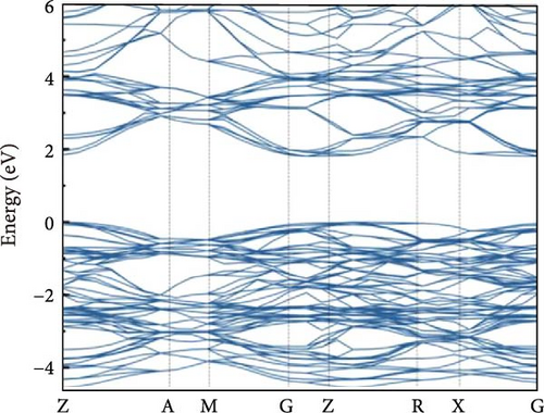
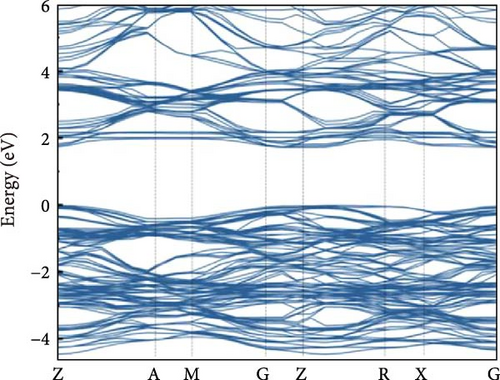
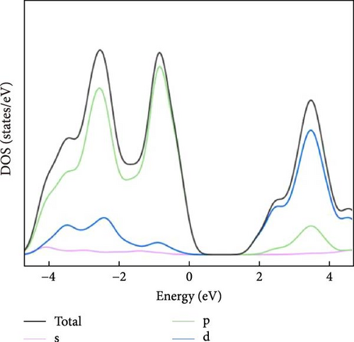
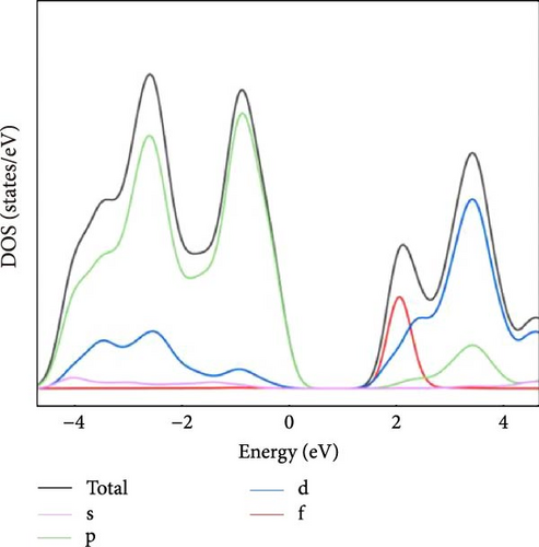
Figures 4(a) and 4(b) show the electronic bandgap structures of pristine BTO and BPTO estimated using DFT with the LDA method. The simulated theoretical bandgap calculation (1.80 eV) was lower than the reported experimental value (3.26 eV). The variation in bandgap values resulting from the implementation of LDA implies the presence of highly correlated electrons of the p–d orbitals and repulsion between anions and cations [56]. The observed decrease in the estimated bandgaps of the pristine and doped BTO samples follows the usual underestimation trend of DFT [57]. BPTO exhibited a slightly lower bandgap of 1.75 eV than BTO (bandgap: 1.82 eV). The partial densities of states were calculated to gain insights into the contributions of the atomic orbitals in both the pristine and doped BTO perovskites. The partial density of states analysis revealed that the upper valence band mainly comprises O 2p orbitals and minor contributions from the Ti 3d and Ba 5p states. Conversely, the conduction band predominantly comprises Ti 3d orbitals and a minor contribution from the O 2p state, as shown in Figure 4(c) [58]. The conduction band edge of BPTO is mainly affected by Ti 3d states hybridized with Pr 4f states, while the valence band is primarily composed of O 2p orbitals [59]. Moreover, Pr doping causes the CB energy levels to degenerate, indicating that resonance levels are formed by Pr 4f orbitals, as illustrated in Figure 4(d) [60]. The incorporation of Pr3+ ions in BaTiO3 lattice leads to the delocalization of 3d and 4f orbital states thereby causing hybridization with Ti 2p and O 2p orbital states. This hybridization between the Pr 4f and host Ti 2p and oxygen orbitals results in the splitting of energy levels creating additional energy states within the bandgap of BTO which can lead to the reduction in the bandgap of Pr doped BTO samples [61, 62]. The impurity levels present in conduction band of Pr-doped BTO lead to decrease in bandgap which can be attributed to the charge compensation after doping [63]. Moreover, when the Pr3+ ions which are slightly smaller ionic radii replace the host Ba2+ ions it causes lattice distortion and strain in the perovskite structure which alters the atomic positions and interatomic distances affecting the overlap and hybridization of orbitals thereby contributing to the decrease in bandgap.
3.4. PL Analysis
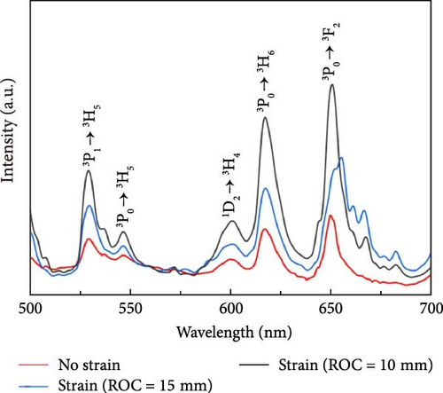
Figure S6(a) depicts the PL spectra of the BTO and BPTO (with different Pr concentrations) samples deposited on the Si substrate. The luminescence observed in lanthanide-doped crystalline materials predominantly originates from electronic transitions occurring within the 4f configuration of the lanthanide dopants. The PL spectra display the characteristic emission band of Pr3+ ions with a maximum intensity at around the red emission range under the excitation wavelength of 325 nm. The PL intensity tended to increase as the Pr3+ ion dopant concentration in the host lattice increased. However, the PL intensity decreased as the Pr concentration increased. This could be attributed to the concentration-quenching effect, which may be caused by nonradiative energy transfer between the Pr3+ ions in the BPTO lattice through exchange interactions or radiation reabsorption [64]. According to Fujiwara et al. [65], the red emission luminescence in Pr-doped CaTiO3, BTO, and SrTiO3 host lattices could be attributed to the distortion arising from the tilted Ti octahedrons within the host lattice. The PL efficiency of rare-earth ions is influenced by symmetry and the strength of the crystal field. A high degree of distortion in the crystal field has been shown to enhance luminescence intensity. Lee and Kim [66] demonstrated that the luminescence efficiency of (Y, Al) NbO4:Yb3+/Er3+ can be improved by tuning the crystal field asymmetry surrounding the rare-earth ions. The emission intensity in BPTO is also influenced by the number of luminous centers and crystal fields surrounding the luminous ions, which are determined by the different lattice symmetries. Consequently, the variation in Pr3+ concentration intensity is attributed to the number of luminous centers. As the number of luminous centers increases, the luminescence intensity gradually increases. Figure S6(b) schematically depicts the luminescence mechanism in BPTO with an energy level diagram of Pr3+ ions. Following the absorption of electrons into the charge–transfer state, some of the excited electrons in the 3P2 level undergo nonradiative multiphonon relaxation to the 3P1, 3P0, and 1D2 states. According to the energy level of Pr3+ ions and the selection rule, the photon energy absorbed by the electrons in the ground state of 3H4 is excited to the 3P2 state when excited by 325 nm wavelength. Since the energy gap between the 3P2, 3P1, and 3P0 levels is small, the 3P1 and 3P0 energy levels will be populated through a nonradiative process. Consequently, recombination to the 3HJ levels (where J = 4, 5, 6) and 3F2 levels occur, and emissions occur because of the characteristic f–f transitions of Pr3+ at specific wavelengths. The PL spectra display peaks at two major regions: (a) the green emission range where the peaks around 530 and 546 nm correspond to the f–f transition of Pr3+ at 3P1→3H5 and 3P0→3H5, respectively, and (b) the dominant red emission range where the peaks around 601, 619, and 650 nm are attributed to the 1D2→3H4, 3P0→3H6, and 3P0→3F2 transitions of Pr3+ ions, respectively.
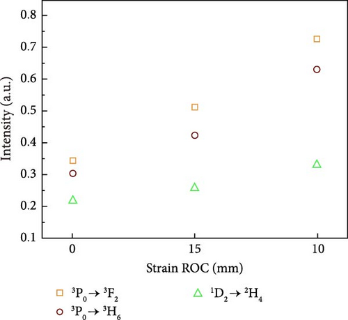
Furthermore, the BPTO sample (0.96 at.%) with optimum intensity was used to examine the strain effect on the PL intensity of the BPTO film deposited on mica substrate. The symmetry and the strength of the crystal field significantly affect the luminescence efficiency of rare-earth ions. It is well established that the distortion of the crystal field has the potential to amplify the luminescence efficiency. PL response is closely related to the structural symmetry of the host and the crystal field around the rare-earth ions. Figure 5(a) illustrates the changes in PL intensity when strain or stress was applied to the flexible mica substrate at different radii of curvature. The host crystal symmetry plays a crucial role in the emission of Pr3+ ions. The 4f 5d band of Pr3+ ions is known to be highly responsive to the crystalline environment of the host lattice. The effect of the crystal field from the host around the Pr3+ ions induces a shift in the Pr 5d energy level, facilitating additional 4f–4f emissions. According to the Judd–Ofelt theory, the increase in the symmetry of the host lattice reduces the crystal field around the Pr3+ ions, thereby diminishing radiative transition. However, the uneven crystal field can mix opposite-parity states into the 4f configuration between the 4f energy levels and the relatively high 4f 5d configuration, thereby leading to an increase in the 4f–4f electric dipolar transition probabilities of the Pr3+ ions. Figure 5(b) shows the red emission spectra under different stress levels. Under mechanical stress, the PL intensity considerably increased around 157.1%, 206.6%, and 211.7% for red emission near 601, 617, and 650 nm wavelengths, respectively.
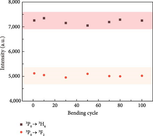
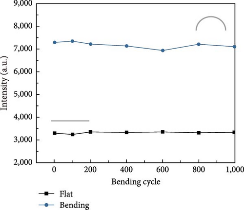
To satisfy the demands of practical applications, it is essential to ensure that the flexible and wearable material exhibits high durability and stability. The red PL emission intensity mainly peaked at 619 and 650 nm (3P0→3H6 and 3P0→3F2) and remained stable for up to 100 bending cycles, as shown in Figure 5(c). A slight fluctuation in PL emission occurred; however, it remained stable over a prolonged bending cycle. A major advantage of this flexible film is that it can achieve a reversible tuning of PL emission. To confirm this capability, a bending test was conducted by measuring the PL intensities of the main peak at about 650 nm under flattening and mechanical strain bending conditions for 103 cycles, as demonstrated in Figure 5(d). The bending fatigue test results demonstrated that the modulation of the PL intensity by strain induced a reversible emission where the PL intensity can be restored to its initial state even after bending. These excellent fatigue resistance properties of our material in both flat and bent states indicate that it is a promising candidate for future multifunctional flexible optoelectronic applications.
3.5. Piezoelectric Properties and Nanogenerator Application
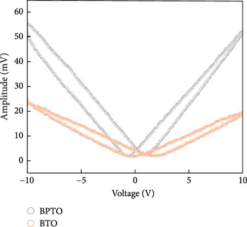
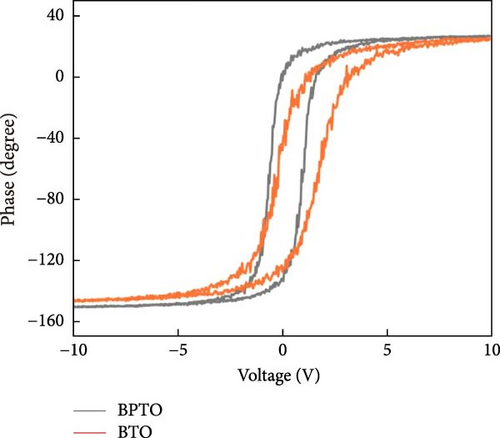
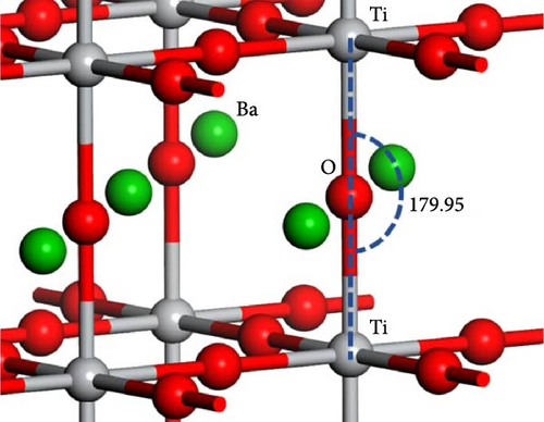
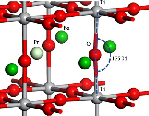
The piezoelectric properties of BTO and BPTO were studied, and their application in nanogenerators was investigated under different forms of stress or strain. BPTO demonstrated a better piezoelectric response than pristine BTO, as shown in Figure 6(a). The piezoelectric behavior enhancement can be attributed to the variation in ionic radii that occurs when the Pr3+ dopant ions replace the Ba2+ ions, which may cause an increase in the field-induced strain by distorting the local host crystal structure. Since Pr exists as Pr3+ ions (which replace the Ba2+ ions) in BTO, this ionic charge difference causes the Pr─O bonds to exhibit stronger polarity than Ba─O. A 180° phase difference can be observed in the phase hysteresis loop, as shown in Figure 6(b), indicating good piezoelectric properties. The effective d33 was calculated using this relationship of Δu = δ × A = d33 × VAC where Δu is the piezo-response displacement, A is the average piezo-response amplitude, δ is the deflection sensitivity of the cantilever, and VAC is the amplitude of the driving voltage [67]. The estimated d33 value was 14.2 and 35.7 pm/V for the BTO and BPTO samples. The improvement in the piezoelectric property due to Pr doping was analyzed based on the structural changes in the simulated DFT structures of BTO and BPTO, as illustrated in Figures 6(c) and 6(d), respectively. When Pr3+ is doped in the Ba2+ site, the ionic size difference that occurs creates lattice distortion, which results in a decrease in crystal symmetry. As observed in the lattice structure, the Ti─O─Ti bond angle decreased from 179.95° to 175.04° after Pr doping, confirming the host lattice distortion. The incorporation of Pr3+ ions induces lattice strain which reduces the symmetry of the host BTO lattice due to the difference in ionic radii. This structural distortion led to a decrease in bandgap accompanied by an increase in piezoelectric property. Doping introduces additional defect states within the bandgap which cause a reduction in bandgap. These defect states increase the electronic polarizability of the BPTO material which contributes to a higher dielectric field in response to an electric field, thereby enhancing its piezoelectric properties [68].
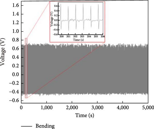
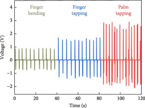
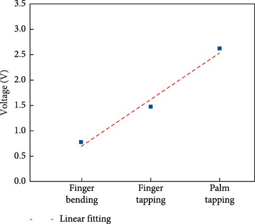
The working principle of the piezoelectric nanogenerator mainly depends on the alignment of dipoles under mechanical stress, as shown in Figure 7(a). When a large electric field was applied, the randomly arranged electric dipoles within the BPTO film aligned along the electric field. Initially, when the nanogenerator was in an equilibrium state, no output voltage was detected without an external force acting on the device. When force was applied to the nanogenerator, the equilibrium was disrupted, inducing piezoelectric charges and creating a potential difference between the electrodes. This potential is due to the change in total polarization within the film. Consequently, positive and negative charges migrate and accumulate at the top and bottom electrodes, respectively, causing the device to generate a positive voltage. When the pressure is released, the piezoelectric potential decreases as the strain decreases, resulting in the migration of accumulated charges in the reverse direction, which produces a negative potential. The resulting back-and-forth flow of free electrons in the external circuit produces an output voltage [69]. The energy-harvesting effectiveness of the prepared BPTO nanogenerator was examined by applying a mechanical strain to the device via different forces. Figure 7(b) shows the output performance of the BPTO-based piezoelectric nanogenerator under bending and releasing conditions. When the film underwent bending or mechanical stress, spontaneous polarization of tetragonal BPTO occurred because of the noncoincidence of the positive and negative charges. The applied force increases the distance between the positive and negative charges, leading to a longer dipole moment in a uniform direction and improving the net polarization. Figure S7 shows the performance of the BTO-based nanogenerator during bending and release. When bent for 5,000 s, BTO exhibited an output voltage of 0.32 V, whereas BPTO exhibited an improved output voltage of about 0.68 V, which can be attributed to its improved piezoelectric behavior after Pr doping. Next, the performance of the BPTO-based nanogenerator was examined under various mechanical forces, as shown in Figure 7(c). The open output voltages generated by finger bending, finger tapping, and palm tapping in the nanogenerator were about 0.75, 1.47, and 2.68 V, respectively. These variations in the output voltage can be attributed to the effects of different pressure levels and the amount of piezoelectric potential produced within the film. The output voltage or current obtained from the thin film was lower than that obtained from the nanocomposite film with a higher thickness. Figure 7(d) clearly shows that the output voltage of the nanogenerator increased linearly as the applied force increased. Therefore, as the applied forces increase, electric displacement within the material also increases owing to the deformation of the crystal structure, resulting in a high polarization density. The long-term durability and stability of our BPTO piezoelectric nanogenerator have been shown in Figures S8(a) and S8(b). The output voltage of the BPTO piezoelectric nanogenerator under bending conditions between the first day and 3 months remains the same. The output voltage shows no significant variation when a palm tapping pressure has been applied to BPTO nanogenerator after 500, 2,000, and 5,000 cycles of bending. These results demonstrate the good stability and durability of our fabricated BPTO nanogenerator. Figure S9(a) shows the increase in output current of the BPTO nanogenerator with increasing mechanical pressure. The sensitivity (S) of our device was calculated according to the linear relationship between the pressure and output current using the formula, S = (Δ(Ip − I0)/I0)/ΔP, where Ip and I0 represent the output current of the device under applied pressure and zero pressure, respectively, and ΔP represents the change in applied pressure [70]. The sensitivity of the device was found to be around 3.2 k/Pa with three different types of pressure applied to the BPTO piezoelectric nanogenerator, as shown in Figure S9(b).

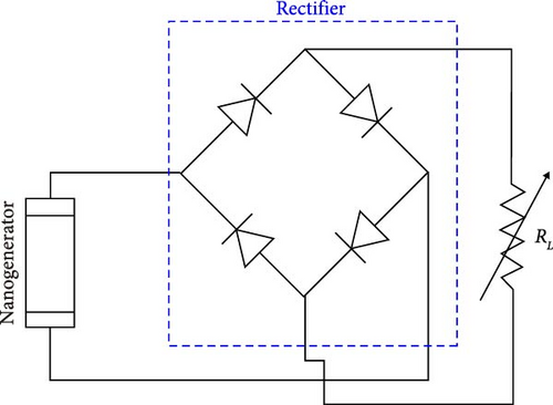
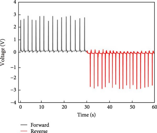
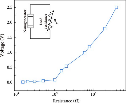
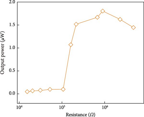
The nanogenerator device offers an alternative source of electrical output that can be effectively utilized as a direct current (DC) source after undergoing rectification. As illustrated in Figure 8(a), four-probe bridge rectifier was used to convert the AC output generated by the nanogenerator into a DC output. When subjected to periodic palm tapping, the rectifying output voltage reached a maximum peak of about 2.8 V in both the forward and reverse biases, as shown in Figure 8(b). Furthermore, to evaluate the practicality of the fabricated piezoelectric nanogenerator, the output voltage and corresponding power generation were measured under various load resistances ranging from 10 kΩ to 6 MΩ. The electrical output of the nanogenerator was measured by connecting the device to a series of electrical resistances, as shown in Figure 8(c) (inset). When the external load resistance exceeded 1 MΩ, the voltage signals peaked at about 2.59 V, similar to the open-circuit voltage. The output instantaneous power of the nanogenerator depends on the load resistance in the system, as illustrated in Figure 8(d). Therefore, the maximum output power of 1.80 μW was obtained at a load resistance of 0.8 MΩ. Table 1 presents the obtained output voltage of our BPTO film, which demonstrates superior performance to previously reported thin-film piezoelectric nanogenerators. This can be attributed to the enhanced piezoelectric properties of the film generated from the lattice distortion by doping the BTO host with Pr. Moreover, our BPTO thin film piezoelectric nanogenerator exhibited superior performance compared to other previously reported rare-earth doped nanogenerator, as shown in Table S1. The effect of Pr doping on thermal and mechanical properties of BTO has been discussed in Figure S10 and Table S2. These results affirm the potential and feasibility of employing BPTO as a multifunctional material for optoelectronic sensing and piezoelectric energy-harvesting applications.
| Material | Deposition method | Film thickness (nm) | Output voltage (V) | Output power (μW) | Reference |
|---|---|---|---|---|---|
| ZnO | Spin coating | 87.6 | 0.66 | 0.0146 | [71] |
| ZnO/NiO | Sputtering | — | 0.43 | — | [72] |
| ZnO | PLD | 800 | 0.09 | 0.0127 | [73] |
|
Sol–gel | 810 | 0.40 | — | [74] |
| KNbO3 | RF sputtering | 300 | 1.8 | 0.106 | [75] |
| (K0.5Na0.5)NbO3 | RF sputtering | 500 | 2.0 | 0.07 | [76] |
| BTO | RF sputtering | 500 | 0.5 | — | [77] |
| BTO | RF sputtering | 300 | 1.0 | 0.025 | [78] |
| BaSrTiO3 | RF sputtering | 520 | 0.50 | 0.108 | [79] |
| Pr:BTO | RF sputtering | 127 | 0.68–2.68 | 1.80 | This work |
4. Conclusion
In summary, we investigated the PL and piezoelectric application potential of a BPTO film that was successfully prepared on a mica substrate using sputtering. The NEXAFS and DFT simulation results confirmed that the bandgap decreased after doping BTO with Pr. During mechanical flexibility tests, the film exhibited high optical transmittance and maintained a stable PL even after 103 bending cycles. The PL behavior of the BPTO film could be modulated by applying mechanical stress at different radii of curvature. A PL enhancement of over 210% was observed in the red emission region when mechanical stress was applied to the film. The lattice distortion in the host lattice not only decreases structural symmetry but also elevates the number of uneven components of the crystal field surrounding Pr3+ ions, which leads to an enhancement in PL emission. Moreover, lattice distortion contributes to an improvement in piezoelectric properties, consequently increasing the voltage output of the piezoelectric nanogenerator. The BPTO-based nanogenerator generated average output voltages of about 0.75, 1.45, and 2.68 V when mechanical force was applied to it through bending, finger tapping, and palm tapping, confirming its ability to harvest energy from different types of applied force. The BPTO device also delivered a maximum output power of around 1.80 μW at an external load resistance of 0.8 MΩ. Therefore, it can be concluded that the BPTO thin film exhibits remarkable performance and could be developed as a promising material for various wearable devices with a dual function of optical sensing and piezoelectric energy harvesting in the future.
Conflicts of Interest
The authors declare that there are no known competing financial interests or personal relationships that could have influenced the work reported herein.
Authors’ Contributions
Akendra Singh Chabungbam and Dong-eun Kim contributed equally to this work.
Acknowledgments
This work was supported by the National Research Foundation of Korea funded by the Korean Government (grant RS-2023-00208801) and the Creative Materials Discovery Program through the National Research Foundation of Korea funded by the Ministry of Science and ICT (grant 2018M3D1A1058536).
Open Research
Data Availability
The data that support the findings of this study are available from the corresponding author upon reasonable request.


