[Retracted] Effect of Gradient Doping on Charge Collection Efficiency of EBCMOS Devices
Abstract
We investigated the effect of different gradient doping methods on the charge collection efficiency of the electron multiplication layer of EBCMOS devices. Exponential doping of the electron multiplication layer can form a built-in electric field in the electron multiplication layer that is favorable for photoelectron transport, so exponential doping instead of uniform doping in the electron multiplication layer of EBCMOS can effectively improve the charge collection efficiency. It is shown that exponential heavy doping on the side of the electron multiplication layer near the dead layer and exponential light doping on the side near the depletion region can improve the built-in electric field structure and increase the lifetime of the multiplied electrons, thereby improving the charge collection efficiency of EBCMOS. The optimized device achieves a charge collection efficiency of 94.48% at an incident electron energy of 4 keV, an electron beam diameter of 20 nm, a dead layer thickness of 60 nm, and a P-type silicon epitaxial layer thickness of 10 μm.
1. Introduction
Current micro-optical imaging devices are mainly divided into ICCD, EMCCD, EBCMOS, and so on [1]. EBCMOS uses a thinned P-type silicon substrate as the electron multiplication layer to replace the traditional ICCD micro-channel plate, fluorescent screen, and coupling device [2], thus making the device size significantly reduced [3]. The electrons generate a large number of electron-hole pairs within the electron multiplication layer, and the obtained electron bombardment semiconductor gain noise is low [4, 5], making the imaging performance of EBCMOS devices far superior to EMCCD devices [6, 7]. With the advantages of small size, low power consumption, fast response, and high resolution [8], EBCMOS devices are widely used in security, biological [9, 10], and medical fields [11, 12].
In 1999, after Intevac published the patent for the EBCMOS device, the first EBCCD with GaAs as the photocathode was subsequently released [13]. After that, because CMOS devices are superior compared to CCD devices, CMOS devices gradually replaced CCD devices [14], and in 2000, Aebi and Boyle [15] developed the world’s first EBCMOS devices [15]. After that, depending on the continuous maturity of CMOS technology, EBCMOS devices began to gradually move towards the trend of high resolution and high frame rate. In 2005 Intevac launched ISIE6 and ISIE10 can reach a high resolution of 1280 ∗ 1024, compared to the previous generation of EBCMOS devices significantly reducing the read noise [16], while the reduced pixel size has also greatly improved the imaging sensitivity of the device [17]. In 2007, the University of Lyon in France, in cooperation with the University of Strasbourg and Photonis, released an EBCMOS device called EBMIMOSA5, which enabled single-photon detection. In 2008, the University of Lyon produced the LUSIPHER [18], a sensor with an increased imaging frame rate from 40 FPS in the EBMIMOSA5 to 500 FPS, which substantially improved single-molecule tracking and allowed the device to be applied in single-molecule tracking experiments. In 2010, Photonis released the EBNoctun1.3Mpx and EBNoctun2Mpx cameras with resolutions of 1.3 and 2 megapixels, respectively. Both can work normally under 10−5lx and can reach 60fps. In 2011, R. Barbier et al. of the University of Lyon used LUSIPHER to achieve single-photon imaging [19]. In 2012, due to its high sensitivity, the University of Lyon used an improved EBCMOS camera system called LuSEApher to achieve deep-sea marine bioluminescence recordings at high frame rates and high sensitivity states [20].
In EBCMOS devices, the incident photoelectrons are accelerated by the accelerating electric field and then enter the BSB-CMOS anode [21], consume a certain amount of energy to cross the dead layer, and then enter the thinned P-type silicon substrate [22], where the photoelectrons collide and scatter with the atoms in the electron multiplication layer, which can be classified into elastic scattering and inelastic scattering according to whether energy is consumed [23]. The elastic scattering process changes the direction of electron motion but does not lose energy while the inelastic scattering process not only changes the direction of electron motion but also loses energy [24]. During inelastic scattering, electrons collide with atoms in the electron multiplication layer, generating a large number of electron-hole pairs. The multiplied electrons are transported to the N-well for collection by diffusion and drift under the action of the electric field and concentration gradient built into the electron multiplication layer and are finally read by the image element circuit [25]. The different doping of the electron multiplication layer determines the distribution of the built-in electric field in the EBCMOS electron multiplication layer. A suitable electric field distribution can increase the electron transport speed and improve the charge collection efficiency. So, the doping of the electron multiplication layer can be changed to improve the charge collection efficiency of the EBCMOS device and thus enhance the imaging level.
In this paper, the effect of different doping methods on the electric field distribution is investigated, and the effect of doping concentration on the minority carriers’ lifetime is also combined with the Monte-Carlo method to obtain the charge collection efficiency under different gradient doping methods, so as to provide a theoretical basis for obtaining EBCMOS devices with high imaging quality.
2. Simulation of the Distribution of Multiplying Electrons in the Electron Multiplication Layer
2.1. Electron Multiplication Process in the Electron Multiplication Layer
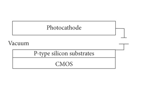
The EBCMOS device uses a photocathode as the cathode of the device and a thin-backed CMOS sensor as the anode of the device [26]. The photocathode and the BSB-CMOS are encapsulated in a vacuum tube [27], the structure of which is shown in Figure 1.
Doping the P-type silicon substrate can generate a corresponding built-in electric field in the electron multiplication layer. Under the effect of the built-in electric field, the multiplication of electrons will accelerate to drift toward the depletion region and be collected by the N-well, thus enhancing the charge collection efficiency.
2.2. Elastic Scattering Model of Incident Electrons in the Electron Multiplication Layer
In the elastic scattering process [35], photoelectrons pass through the dead layer and collide with the nucleus. The energy loss of the incident electrons during the whole process is so small that it can even be negligible. We analyze the collisions for a single atom using the classical Rutherford formula, which can then be extended to the elastic scattering process for all atoms.
2.3. Inelastic Scattering Model of Incident Electrons in the Electron Multiplication Layer
It is known that KAl = 0.815 and Kc = 0.77, and bringing in the known values gives KSi = 0.822.
2.4. The Trajectory of Electrons in the Electron Multiplication Layer
In the process of elastic scattering calculation, it is only necessary to consider the relative change of coordinates at the end of each process compared to the coordinates after the previous scattering, calculate this cumulatively in the z-direction, and stop the calculation when the distance in the z-direction is greater than the thickness of the electron multiplication layer [41].
In the inelastic scattering process, not only the orientation of the electron scattering motion should be calculated but also the energy lost in the single inelastic scattering process should be calculated at the same time. After each inelastic scattering process calculation, the remaining energy of the obtained electron will be used as the initial energy for the next calculation, and the position of the obtained electron will be used as the initial position for the next calculation, and if the electron energy is less than 3.6 eV, the calculation will be stopped at this time.
3. Electric Field Distribution inside the Electron Multiplication Layer with Different Doped Methods
3.1. Distribution of Electric Field in Electron Multiplication Layer with Uniformly Doped Methods
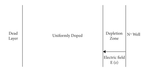
In the depletion region, the effect of the built-in electric field makes the electron migration velocity much faster than the electron diffusion velocity, and the electron migration is accelerated toward the N-well.
3.2. Distribution of Electric Field during Exponential Doping of Electron Multiplication Layer
We found that when the p-type silicon substrate is uniformly doped, there is only an electric field distribution in the depletion region, and the multiplication of electrons in the electron multiplication layer only depends on the concentration gradient for diffusion. At this time, increasing the transport velocity of multiplier electrons can reduce the recombination rate of electron-hole pairs, thus increasing the charge collection efficiency. In order to enhance the transport velocity of multiplier electrons, a gradient electric field can be generated at the P-type silicon substrate by exponential doping of the P-type silicon substrate, and the electric field distribution at this time is shown in Figure 3. Different gradient index doping methods have a significant effect on the distribution of the electric field outside the depletion region [42], so changing the gradient index doping method can effectively improve the charge collection efficiency.
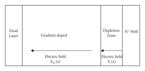
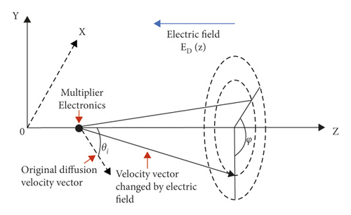
D n is the diffusion coefficient, the carrier diffusion length , τ is the lifetime of the nonequilibrium carrier, Ln(E) = (μnEτ/cosθi), vE(z) = μn · E, μn is the electron mobility, and the electron mobility is related to the doping concentration.
When the electron multiplication layer is exponentially doped, the motion trajectory of the multiplication electrons is shown in Figure 4. When v(z) < 0, the multiplier electrons move toward the dead layer and are finally compounded; when v(z) > 0, the multiplier electrons move toward the N-well and are finally collected.
4. Charge Collection Efficiency under Different Gradient Doping Methods and Discussion
According to the semiconductor theory, by combining the parameters such as lifetime, depletion region width, and diffusion coefficient of nonequilibrium carriers under different gradient doping methods, the trajectories of corresponding multiplier electrons in the substrate can be obtained, and finally, the charge collection efficiency under different gradient doping can be obtained. In the simulation parameters, the incident electron energy is set to 4 keV, the electron beam diameter is 20 nm, the dead layer thickness is 60 nm, and the thickness of the P-type silicon epitaxial layer is 10 μm.
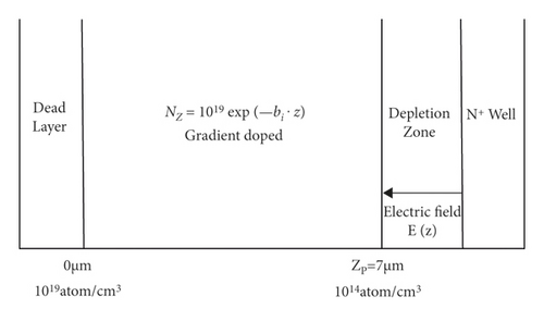
At 0 < z < 7, the overall exponential doping is performed with NZ = 1019exp(−bi · z) and N7 = 1014atom/cm3. Figure 5 shows the electron multiplication layer model for this doping method.
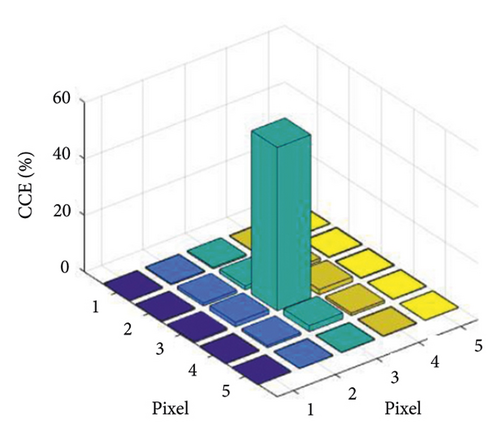
At this time, the electron distribution in the 5 × 5 region is shown in Figure 6, and the final obtained charge collection efficiency is 54.74%.
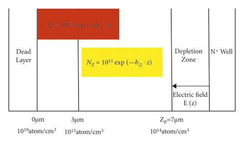
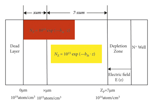
At 0 < z < 3, exponential doping is performed with NZ = 1019exp(−bi1 · z), and at 3 < z < 7, exponential doping is performed with NZ = 1015exp(−bi2 · z), N3 = (1015atom/cm3). Figure 7 shows the electron multiplication layer model for this doping method.
The electron distribution in the 5 × 5 region at this time is shown in Figure 8, and the final charge collection efficiency obtained is 70.35%.
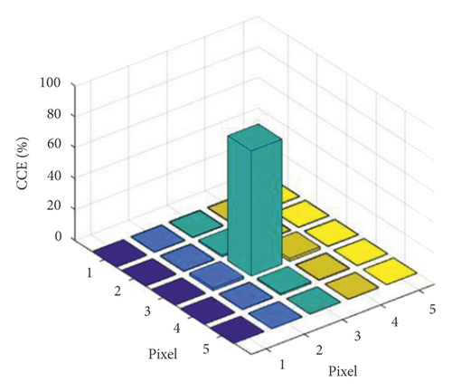
With this doping, the charge collection efficiency reaches 70.35%. In order to enhance the nonequilibrium carrier lifetime, we will try to further thin the thickness of the exponential heavily doped layer to achieve the effect of increasing the charge collection efficiency.
At 0 < z < 0.5, exponential doping is performed with NZ = 1019exp(−bi3 · z), and at 0.5 < z < 7, exponential doping is performed with NZ = 1015exp(−bi4 · z), N0.5 = (1015atom/cm3), and Figure 9 shows the model of electron multiplication layer for this doping method.

The electron distribution in the 5 × 5 region at this time is shown in Figure 10, and the final charge collection efficiency obtained is 86.35%.

It can be seen that a thin exponential heavily doped layer near the dead layer side can effectively improve the charge collection efficiency. We further thinned the thickness of the exponentially heavily doped layer, and the model of the electron multiplication layer is shown in Figure 11, and the relationship between the thickness of the exponentially heavily doped layer and the charge collection efficiency is given in Table 1.
| Thickness | 0.3 | 0.2 | 0.1 | 0.05 | 0.03 | 0.01 |
|---|---|---|---|---|---|---|
| CCE | 89.42% | 91.88% | 94.48% | 93.11% | 90.14% | 81.66% |
Analyzing these results, it is clear that the thinning of the exponentially heavily doped layer is beneficial to enhance the charge collection efficiency, and NZ = 1019exp(−bia · z) for heavy exponential doping when 0 < z < 0.1, NZ = 1015exp(−bib · z) for light exponential doping when 0.1 < z < 7, and N0.1 = 1015atom/cm3, at which the maximum charge collection efficiency of 94.48% is obtained. At this point, if the thickness of the exponentially heavily doped layer is further reduced, the charge collection efficiency starts to gradually decrease, which we speculate because an excessively thick exponentially lightly doped layer makes the strength of the gradient electric field in the exponentially lightly doped layer decrease, along with the increase in the thickness of the exponentially lightly doped layer, which makes the drift rate of the nonequilibrium carriers decrease and increases the compound rate of the electron-hole pairs, which eventually makes the charge collection efficiency affected.
5. Conclusion
Based on semiconductor theory, a computational model was developed to determine the effect of different doping methods on the charge collection efficiency in EBCMOS. When the P-type silicon substrate is uniformly doped, an electric field exists only in the depletion region, and no electric field can be generated at the electron multiplication layer. Exponential doping of P-type silicon substrates can produce a gradient electric field that facilitates the transport of multiplying electrons. If the P-type silicon substrate is exponentially doped as a whole, the high impurity concentration in the electron multiplication layer reduces the minority carriers’ lifetime and the obtained charge collection efficiency is low. To solve this problem, we designed a multistage exponential doping structure of the electron multiplication layer. The thinner heavy exponential doping layer reduces the compounding probability of multiplying electrons in this region, while the suitable doping structure ensures the strength of the built-in electric field and the diffusion of multiplying electrons. Set the incident electron energy to 4 keV, the electron beam diameter to 20 nm, the dead layer thickness to 60 nm, and the thickness of the P-type silicon epitaxial layer to 10 μm. The simulation results show that the thinner exponential heavily doped layer can obtain the ideal charge collection efficiency in the range of 0 < z < 0.1 μm with NZ = 1019exp(−bia · z), and in the range of 0.1 < z < 7 μm with NZ = 1015exp(−bib · z) for exponential doping with N0.1 = 1015atom/cm3, when the maximum charge collection efficiency of 94.48% was obtained.
Conflicts of Interest
The authors declare that they have no conflicts of interest.
Open Research
Data Availability
The dataset can be accessed upon request.


