Volume 2018, Issue 1 8490740
Research Article
Open Access

A Quad-Element UWB-MIMO Antenna with Band-Notch and Reduced Mutual Coupling Based on EBG Structures

Wenjing Wu

Wenjing Wu

Institute of Antenna and Microwave Technology, Hangzhou Dianzi University, Hangzhou 310018, China hdu.edu.cn

Search for more papers by this author
Bo Yuan

Corresponding Author

Bo Yuan

Institute of Antenna and Microwave Technology, Hangzhou Dianzi University, Hangzhou 310018, China hdu.edu.cn

Search for more papers by this author
Aiting Wu

Aiting Wu

Institute of Antenna and Microwave Technology, Hangzhou Dianzi University, Hangzhou 310018, China hdu.edu.cn

Search for more papers by this author
First published: 25 February 2018
Citations: 86
Academic Editor: Giorgio Montisci

Abstract

A compact planar quad-element ultrawideband (UWB) antenna with a band-notch and low coupling for multiple-input multiple-output (MIMO) system is proposed in this paper. The antenna consists of four circular monopoles with modified defected ground plane and a periodic electromagnetic band gap (EBG) structures. The proposed EBG structures are modified from the traditional mushroom-like ones, comprised of patterns of grids on the top patch, the metallic ground plane, and several vias that connect the top and bottom plane. It is printed at the center of the dielectric substrate to lower electromagnetic coupling between the parallel elements. Besides, by etching four crescent ring-shaped resonant slots on the radiators, a sharp band-notched characteristic is achieved. From the experimental results, the −10 dB bandwidth of the antenna is extended covers from 3.0 to 16.2 GHz, with a sharp notched band at 4.6 GHz. And the isolation is greater than 17.5 dB between its elements, with a peak gain of 8.4 dB and a peak efficiency of 91.2%. Moreover, it has a compact size of 0.6λ × 0.6λ × 0.016λ at 3 GHz and could be a good candidate for portable devices.

1. Introduction

Since Federal Communications Commission (FCC) released the spectrum from 3.1 to 10.6 GHz for commercial applications [1], ultrawideband (UWB) technology has drawn considerable attention due to its merits of low complexity, low-power consumptions, capability of high data rate, low interference, good time-domain resolution, and reduction of severe multipath effect [2]. Although UWB communication system makes use of huge frequency bands, the permitted power spectral density of the UWB signal is rather limited to avoid interference with other systems, such as the frequency band from 4400 to 4990 MHz, which is adopted in large capacity microwave relay trunk network. Multiple-input-multiple-output (MIMO) technology enables the transmission of data over multiple channels and increases the channel capacity without additional power requirements; thus, it has been widely used in modern wireless communication system [3]. Furthermore, compact and planar antenna designs are of great demand since they are easier to integrate with wireless devices [4].

As a key technology for next-generation communication systems, MIMO technique can increase the capability and reliability without additional power or spectrum [5]. To achieve good performance and compact structure, good isolation between closely-spaced antennas is required for MIMO communication systems [6]. In [4], a compact quad-element wideband antenna with slotted ground plane is presented. By etching a modified slotted ground plane, the bandwidth is extended covers from 2 to 6 GHz with a compact size of 0.33λ × 0.33λ × 0.01λ at 2 GHz, but the isolation is only 14 dB between its elements. In [7], a wideband MIMO antenna with common elements suitable for WiFi and LTE wireless access point application is proposed. It consists of four microstrip feedline-printed monopole antennas with common radiating element and a ring-shaped ground plane; the impedance bandwidth is enhanced from 1.8 to 2.9 GHz by common element particular design. However, it only results in isolation of 15 dB in the operating frequency band. In [8], a four-element MIMO patch antenna is designed for 2.45 GHz band operation. For the purpose of antenna miniaturization, it adopts complementary split-ring resonator (CSRR) loading on its ground plane, which reduces the single-element antenna size by 76%. But, the isolation of the antenna only achieves −10 dB. In [9], a dual element stacked patch antenna is designed for MIMO technology, it achieves a high isolation, and the minimum isolation reaches 31 dB mainly due to the orthogonal polarization modes of the two excited ports. Nevertheless, the relative operating frequency bandwidth is only 4.3% from 3.65 to 3.81 GHz and the overall dimension is 0.99λ × 1.05λ × 0.03λ at 3.65 GHz which is obviously large in miniaturization portable devices.

In this paper, a compact UWB-MIMO antenna with a band-notch and reduced mutual coupling is presented and fabricated. The initial design of a single element includes a circular monopole at the top layer of the dielectric substrate and a modified defected ground structure at the bottom layer to obtain an ultrawideband. Besides, a crescent ring-shaped resonant slot is etched on the surface of the circular monopole to achieve a band-reject to inhibit the interference of large capacity microwave relay trunk network. The orthogonal placement of the elements can ensure the low coupling between the orthogonal element (e.g., 1-2 and 1–4) and a 3 × 3 array electromagnetic band gap (EBG) structure can ensure high isolation between the parallel elements (e.g., 1–3 and 2–4). From the experimental results, the proposed antenna has ultrawideband covers from 3.0 to 16.2 GHz, the band-notch centered at 4.6 GHz covers from 4.0 to 5.2 GHz, and good isolation of 17.5 dB between every two elements is achieved. Besides, radiation pattern, gain, efficiency, envelope correlation coefficient (ECC), total active reflection coefficient (TARC), mean effective gain (MEG), diversity gain (DG), and channel capacity loss (CCL) are measured and calculated.

2. Proposed Antenna Configuration

The proposed antenna is fabricated on the low-cost FR4 substrate with a relative permittivity of 4.4, thickness of 1.6 mm, and loss tangent of 0.02. Electromagnetic simulator HFSS is used for calculating S-parameters, gain, efficiency, radiation pattern, ECC, TARC, MEG, DG, and CCL, while the dispersion characterization of surface waves propagating on the EBG structures is investigated by CST MWS.

2.1. Single-Element Antenna
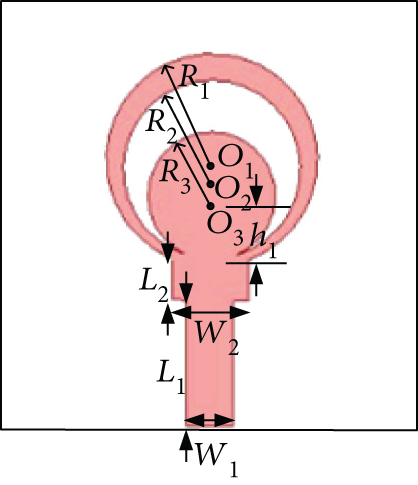
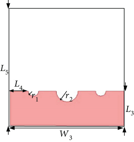
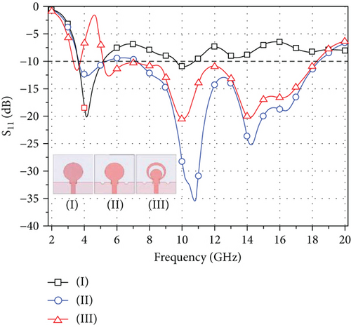
The geometry of a single element of the four port antenna is shown in Figure 1. The evolution of the element to obtain an ultrawideband and a band-notched at 4.6 GHz is shown in Figure 2. A printed circular monopole is adopted as the basic element for the antenna; from Figure 2, one can conclude that it radiates at 4.0 GHz and with a bandwidth of 1.46 GHz. The shape of the ground plane of the circular monopole radiator is a rectangle with dimensions of W3 × L3, as shown in Figure 2 (case I). To achieve an ultrawideband resonance, a big semicircle with radius of r2 and two small semicircles with radius of r1 are etched on the rectangle ground. The circular monopole radiator benefits from this defected ground structure which has an effect on impedance matching; thus, its simulated bandwidth is expanded covers from 3.3 to 18.0 GHz below −10 dB impedance bandwidth level, which is shown as case II in Figure 2. In order to inhibit the interference of large capacity microwave relay trunk network, a crescent ring-shaped resonant structure is etched on the surface of the circular monopole antenna as shown in case III in Figure 2. The slot acts as a quarter (guided) wavelength parallel open-circuit transmission line that shorts the antenna at the frequency band from 4.0 to 5.2 GHz. The band-notch characteristics at the frequency band are obtained by etching a crescent ring-shaped resonant slot from the circular monopole of the antenna. The length of the slot is about λ/2 at the center frequency of the notched band and can be calculated by the following formulas:
()
where LL2 is the outer arc length of the etched slot that can be derived by trigonometric function of other geometric parameters as follows: LL2 = 2(π − arccos((h1 + d2)/R2))R2, the geometric meanings of parameters h1, d2, and R2 are illustrated in Figure 1(a), and π and arccos((h1 + d2)/R2) are in radian measurement; LL3 represents the inner arc length of the etched slot, its mathematical formula as follows: LL3 = 2(π − arccosh1/R3)R3, h1, and R3 are also illustrated in Figure 1(a), and arccos(h1/R3) is in radian measurement too; c is the speed of the light; fcenter is the center frequency of the notched band; the value of relative permittivity εr is 4.4; εeff is effective dielectric constant of the microstrip, and it is simplified from a formula for dielectric constant of the uniform medium. According to the center frequency of 4.6 GHz, the parameters of R2, R3, d2, and h1 are calculated initially. Then, the parameters are optimized as R2 = 5.7 mm, R3 = 4.1 mm, d2 = 0.7 mm, and h1 = 4.0 mm by HFSS.
Details are in the caption following the image
Geometry and parameters of a single element. (a) Front view. (b) Back view. Dimensions (unit: mm): W1 = 3.0, L1 = 8.0, W2 = 4.9, L2 = 2.7, h1 = 4.0, R1 = 6.8, R2 = 5.7, R3 = 4.1, W3 = 28.5, L3 = 8.8, L4 = 4.5, L5 = 28.5, r1 = 1.3, and r2 = 2.75. Note. O1, O2, and O3 are the center of the circle with radius R1, R2, and R3, respectively. The following are the distances: d1 = |O1O2| = 0.6 and d2 = |O2O3| = 0.7.
Details are in the caption following the image
Evolution of single element of UWB-MIMO antenna and its S11 characteristics.

2.2. Integration of a Four-Element Antenna

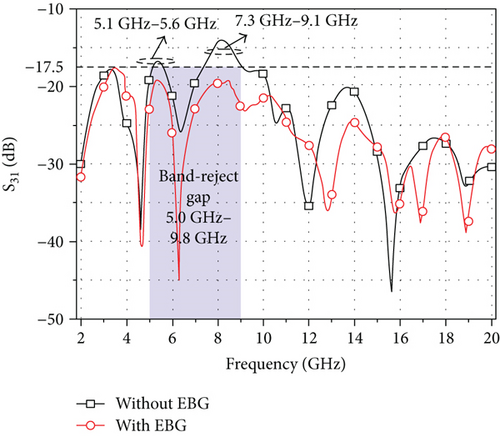
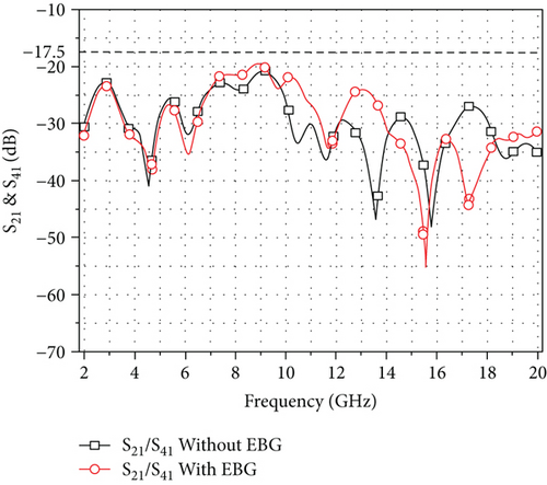
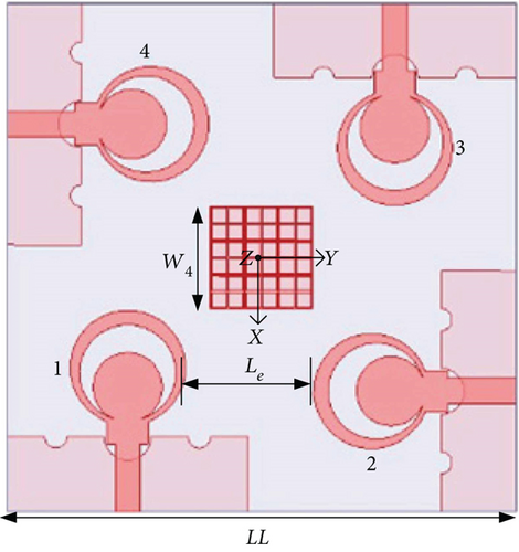
By using the element proposed in the previous section, a simulated model of a quad-element UWB-MIMO antenna is built as shown in Figure 3(a). Individual elements, occupying an area of 0.08λ2, are placed rotationally and symmetrically in a square substrate with an interval of 90°. As illustrated in Figure 4, the S-parameters between parallel element (i.e., 1–3 and 2–4) exhibit a suppressed isolation, overwhelmingly lower than 17.5 dB in the frequency band of 5.1 GHz–5.6 GHz and 7.3 GHz–9.1 GHz. However, the orthogonal arrangement of elements (i.e., 1-2 and 1–4) exhibits good isolation, which is mainly greater than 20 dB in the whole band. The orthogonal arrangement of elements in the antenna can ensure a good isolation between adjacent elements, which is due to the orthogonal polarization field produced in the elements and the mutual coupling is reduced. However, the parallel elements can produce the symmetrical electromagnetic field and the similar polarization; thus, the power will flow from antenna 1 to antenna 3 (antenna 2 to antenna 4) when they are excited, which leads to the high coupling between parallel elements. In Section 3, the EBG structures are proposed to inhibit the mutual coupling between the parallel elements.
Details are in the caption following the image
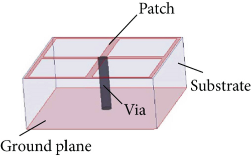
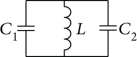
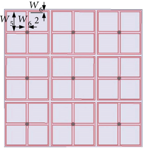
(a) Geometry and parameters of a four-port UWB-MIMO antenna. (b) A 3 × 3 EBG array structure. (c) Geometry of a unit cell. (d) Parameters of a unit cell. (e) The equivalent parallel LC resonant circuit. Dimensions (unit: mm): W4 = 12.1, LL = 60, Le = 15.3, W5 = 1.75, W6 = 0.2, W = 3.9, g = 0.1, h = 1.6, and r = 0.15.
Details are in the caption following the image
The comparison of the simulated isolations with and without EBG structures. (a) Isolation of the parallel-element: S31. (b) Isolation of the orthogonal-element: S21/S41.
Details are in the caption following the image
The comparison of the simulated isolations with and without EBG structures. (a) Isolation of the parallel-element: S31. (b) Isolation of the orthogonal-element: S21/S41.

2.3. Investigation of Band-Reject Gap Properties

As it is well known, EBG structures can suppress wave propagation in the space between the elements and produce a band-reject gap. Therefore, a periodic EBG structure is implemented to inhibit the mutual coupling between the parallel elements with the target frequency band of 5.1–5.6 GHz and 7.3–9.1 GHz. The 3 × 3 EBG array structures, unit cell structure, geometrical parameters of the unit cell, and the parallel LC equivalent resonant circuit are shown in Figures 3(b)3(e), respectively. The operation mechanism of this EBG structure can be explained by an equivalent LC resonant circuit: C1 is the capacitance of air gap between adjacent EBG unit cells, C2 is the capacitance of dielectric gap between top metallic patch and ground plane, and L represents the inductance of metallic vias. For an EBG structure with patch width W, gap width g, substrate thickness h, and dielectric constant εr, the values of the inductor L and the capacitors (i.e., C1 and C2) are determined by the following formulas [10]:
()
where W ≈ (1 − 2S/W2)W, S = π r2, a = W + g, C = C1 + C2 and S represents the cross-sectional area of via hole, μ0 is the permeability of free space, and ε0 is the permittivity of free space. The initial parameters of the unit cell are calculated by (2), according to the frequency band of 5.1–5.6 GHz and 7.3–9.1 GHz. Then, dispersion diagram is drawn to further study the high-impedance surface of the EBG structures.

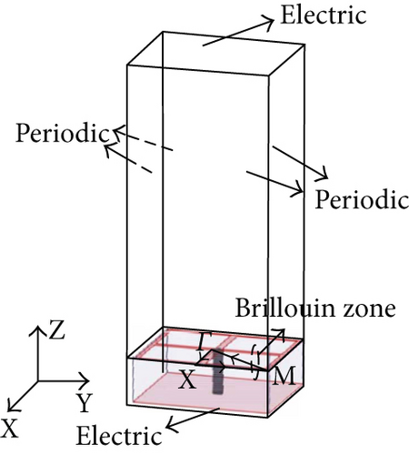
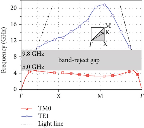
According to the initial parameters of the unit cell, dispersion characterization of surface waves propagating on the unit cell of EBG structures is investigated using finite integration technique (FIT) by CST MWS. The boundary conditions of side walls of the unit have to be considered periodic, and the boundaries at the top and the bottom of the model are defined as electric conductor, as illustrated in Figure 5(a). In order to cover the frequency band of 5.1–5.6 GHz and 7.3–9.1 GHz, the parameters of the unit cell are optimized as follows: W5 = 1.75 mm, W6 = 0.2 mm, W = 3.9 mm, and g = 0.1 mm. The numerically simulated kβ dispersion diagram of the surface modes propagating in the EBG structure is conducted using CST eigenmode solver, as shown in Figure 5(b). A complete band-reject between the first mode (TM0 mode) and the second mode (TE1 mode) in the frequency band of 5.0–9.8 GHz can be observed.Γ, X, and Mstand for symmetric points in the irreducible Brillouin zone. The Γ − X branch represents βxa/π with βy = 0, the XM branch represents βya/π with βx = π/a, and the M − Γ branch represents βxa/π with βx = βy [1014]. Because of slow-wave behavior of surface waves, dispersion curves are calculated only in the region under the light line, and the simulated frequency band-reject gap is from 5.0 to 9.8 GHz, as shown in Figure 5(b). Therefore, the isolation between the parallel elements has been enhanced from 17 dB to 20 dB within the band-reject gap of 5.1–5.6 GHz and 7.3–9.17 GHz when the 3 × 3 EBG array structures placed at the center of the dielectric substrate, which could be observed in Figure 4(a).
Details are in the caption following the image
The band-reject gap property of the mushroom-like EBG structure. (a) The settings of a unit cell in CST MWS. (b) Simulated surface wave band structure for a unit cell.
Details are in the caption following the image
The band-reject gap property of the mushroom-like EBG structure. (a) The settings of a unit cell in CST MWS. (b) Simulated surface wave band structure for a unit cell.

3. Measurement and Results

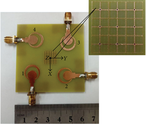
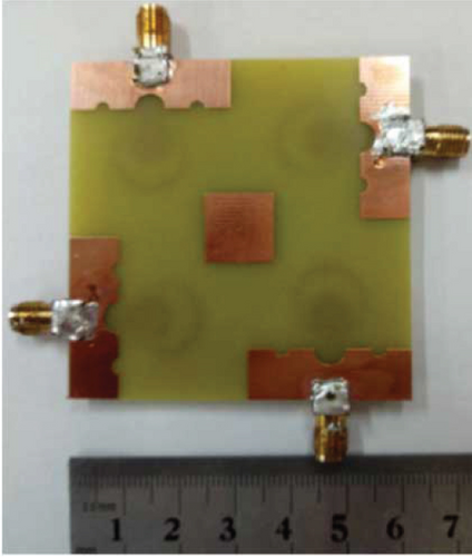
The proposed antenna is fabricated, as shown in Figure 6. Simulated and measured results of the quad-element UWB-MIMO antenna system are discussed in this section. The measurements of the proposed antenna are implemented by using Rohde and Schwarz ZVM vector network analyzer.
Details are in the caption following the image
Photographs of fabricated proposed antenna. (a) Front view. (b) Back view.
Details are in the caption following the image
Photographs of fabricated proposed antenna. (a) Front view. (b) Back view.

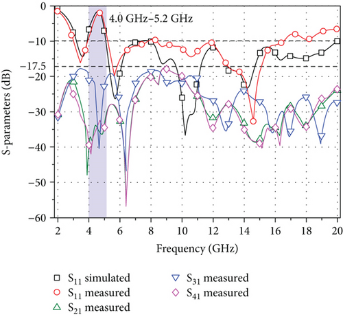
The simulated and measured S-parameters of the UWB-MIMO antenna are shown in Figure 7. The measured S-parameter under −10 dB level is from 3.0 to 16.2 GHz with a bandwidth of 137.5%, which is less than the simulated one from 3.0 to 20.0 GHz. Deviation of S11 curve occurs at high-frequency band between the measured result, and the simulated one is mainly due to the error of fabricating, welding, and testing. And reflection coefficient of the band-notched antenna at 4.6 GHz is about −2.4 dB, which can inhibit the interference of large capacity microwave relay trunk network from 4.0 to 5.2 GHz. From the curves of S-parameters, it can be observed that the antenna system exhibits a measured minimum isolation of 17.5 dB between its elements throughout the operating band. A comparison between the proposed antenna and few other recently reported planar MIMO designs in terms of bandwidth, mutual coupling, and size is shown in Table 1, where λ0 is the largest free-space wavelength corresponding to the lowest operating frequency of the referenced antennas. It can be observed that the proposed planar MIMO antenna has an excellent bandwidth performance, a good inhibitory ability to rejected frequency band, and has a compact size.
Details are in the caption following the image
The measured and simulated S-parameters of the fabricated four port MIMO antenna.
Table 1. Comparison with other MIMO antennas.
Ref. Element number −10 dB bandwidth (%) Minimum isolation (dB) Total area
[4] 4 96.2 14 0.11
[7] 4 46.8 15 0.60
[8] 2 131.0 15 0.34
[9] 2 4.3 31 1.03
[10] 4 23.9 14 0.43
This work 4 137.5 17.5 0.36

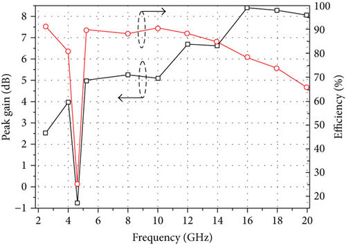
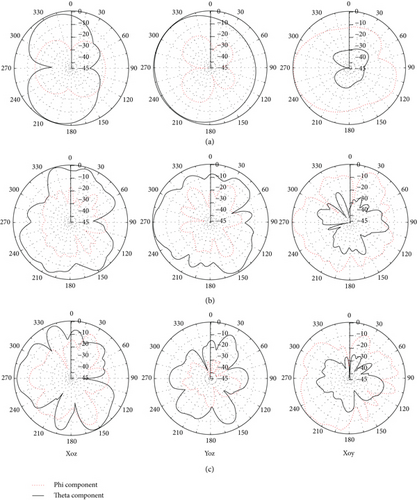
Far-field patterns are obtained inside an anechoic chamber for antenna 1, while the other three elements are terminated with 50 Ω impedances. Port 1 is measured due to the symmetrical of the proposed antenna, which leads to the same patterns when other ports are excited. Measured radiation patterns for xoz-plane, yoz-plane, and xoy-plane at 3.5, 10.5, and 16.2 GHz are shown in Figure 8. It is observed that cross-polarization at some planes is quite high because of the orthogonal arrangement of the four elements, which leads to the orthogonal of the electrical field. Peak gain and efficiency measurements are also performed and are plotted in Figure 9. Gain measurements show a peak gain of 8.4 dB at 16 GHz, and a peak efficiency of 91.2% is obtained at 10 GHz.
Details are in the caption following the image
Measured radiation pattern of the proposed antenna at (a) 3.5, (b) 10.5, and (c) 16.2 GHz (at two planes of xoz and yoz, where theta component is coplanar radiation pattern; and at xoy plane, where phi component is coplanar radiation pattern).
Details are in the caption following the image
Measured gain and efficiency of the proposed antenna.
The envelope correlation coefficients (ECC), diversity gain (DG), and total active reflection coefficient (TARC) are computed for evaluating the diversity performance of the proposed quad-element MIMO antenna. ECC quantifies the correlation between the branch signals received by different elements, and a lower ECC signifies higher pattern diversity. The envelope correlation coefficient ρe of the four-antenna system can be given by [15]
()
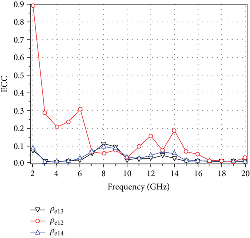
where XPR is the ratio of cross-polarization power, which is defined as XPR = PV/PH (PV and PH are the vertical component strength of the electric field and the horizontal component strength of the electric field, resp.). Eθi and EΦj are the complex envelops of θ and Φ component of far-field radiation patterns, respectively, when the ith port is excited and the other ports are terminated with 50 Ω impedance. Pθ and PΦ are the probability distributions of the power incident on the antenna in the θ and Φ polarizations, respectively. The angle Ω is defined by θ in elevation and Φ in azimuth. ECC is below 0.3 in the working frequency band from 3.0 to 16.5 GHz as shown in Figure 10, and that could ensure the favorable diversity gain (DG) presented in Table 2. TARC is the square root of the sum of all incident powers at the ports minus radiated power and then divided by the sum of all incident powers at the ports of an N-port antenna. TARC can be computed by the following formula, given by [8]
()
()
where ai and bi are the incident signals and reflected signals, respectively, [S] is the antenna’s scattering matrix, [a] is the excitation vector, and [b] represents the scattered vector. Formula (5) can be written as
()
Details are in the caption following the image
Simulated ECCs between the elements of the antenna.
Table 2. Meg and DG of MIMO antenna system.
MEG1 (dB) MEG2 (dB) MEG3 (dB) MEG4 (dB) DG (ρe12) DG (ρe13) DG (ρe14)
XPD 0 dB 6 dB 0 dB 6 dB 0 dB 6 dB 0 dB 6 dB
3G −3.6 −5.7 −3.5 −5.6 −3.7 −5.8 −3.6 −5.6 6.0 dB 4.4 dB 6.2 dB
9G −3.5 −6.6 −3.4 −6.5 −3.6 −6.7 −3.4 −6.7 10.4 dB 10.3 dB 10.2 dB
15G −4.1 −7.8 −4.0 −7.9 −4.2 −7.7 −4.2 −7.7 8.7 dB 8.5 dB 8.8 dB

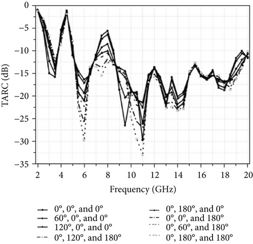
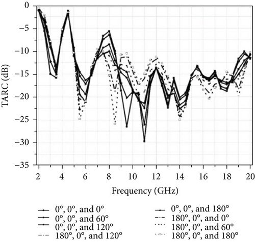
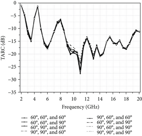
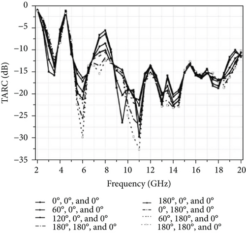
According to the four-port MIMO antenna system, TARC is a parameter that refers to the coupling of the ports, and its value is between 0 and 1, where 0 means all incident power is radiated, but 1 means all incident power is reflected. TARC curves for the proposed MIMO antenna with different phase combinations between the four elements are described in decibels in Figure 11. The excited port 1 is kept at 1ej0, while the other ports (i.e., ports 2, 3, and 4) are excited with different phases. For example, if the legend reads (120°, 180°, and 0°), it means that the excited phase of antenna 2 is at 120° shift with antenna 1, antenna 3 is at 180° shift, and antenna 4 is consistent with antenna 1. As evident from the figures, the simulated TARC curves have an agreement with the S11 curve at some phases shift (e.g., 180°, 0°, and 0°, 0°, 180°, and 0°, and 0°, 0°, and 180°) of the excited ports, where more incident power is radiated.
Details are in the caption following the image
TRAC curves for the proposed MIMO antenna with different phase combinations between the four elements: (a) elements 1 and 4 are in phase; (b) elements 1 and 2 are in phase; (c) elements 1 and 3 are in phase; (4) all elements are out of phase.
Details are in the caption following the image
TRAC curves for the proposed MIMO antenna with different phase combinations between the four elements: (a) elements 1 and 4 are in phase; (b) elements 1 and 2 are in phase; (c) elements 1 and 3 are in phase; (4) all elements are out of phase.
Details are in the caption following the image
TRAC curves for the proposed MIMO antenna with different phase combinations between the four elements: (a) elements 1 and 4 are in phase; (b) elements 1 and 2 are in phase; (c) elements 1 and 3 are in phase; (4) all elements are out of phase.
Details are in the caption following the image
TRAC curves for the proposed MIMO antenna with different phase combinations between the four elements: (a) elements 1 and 4 are in phase; (b) elements 1 and 2 are in phase; (c) elements 1 and 3 are in phase; (4) all elements are out of phase.
To quantify the average received signal strength for each element, mean effective gains (MEGs) are calculated as the ratio of mean received power to the mean incident power. The MEG of the antenna can be calculated using its two-dimensional gain pattern, which is given by [8] as
()
where Γ is the cross-polarization discrimination (XPD) of the incident field, Gθ and GΦ are the power gain patterns. The MEG of the proposed antenna is tabulated in Table 2. An XPD of 0 dB corresponds to outdoor applications and an XPD of 6 dB corresponds to indoor applications. As evident from the Table, the antenna has a good MEG performance as deviations between the MEGs of the various elements are both less than 3 dB.
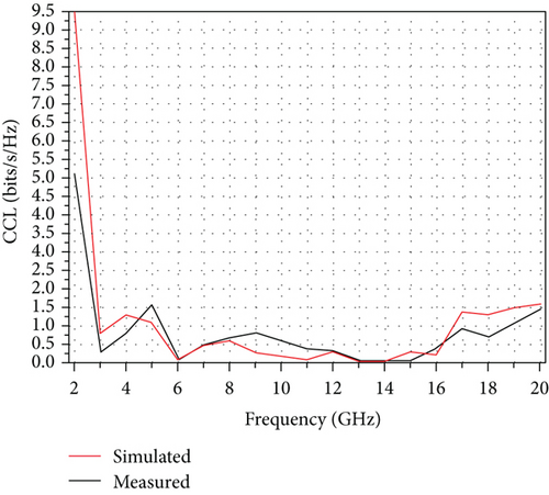
Theoretically, the channel capacity can be improved by increasing the number of antennas of the MIMO system. However, the uncorrelated Rayleigh fading will result in channel capacity loss (CCL) of the MIMO system. The capacity loss (Closs) of the four-element MIMO antenna can be evaluated by using the equation as follows [16, 17]:
()
where ψR is the receiving antenna correlation matrix that is given by
()
, and , for i, j = 1, 2, 3, or 4. The simulated and measured capacity losses of the proposed MIMO antenna are shown in Figure 12; it can be seen that the simulated capacity loss is less than 0.4bits/s/Hz in the operating frequency band except for the frequency band of 3.0 GHz–5.7 GHz and 7.0 GHz–8.3 GHz. Observed from Figure 4 and Figure 9, the isolation of parallel element is 2 to 4.5 dB lower in the band of 3.0 GHz–3.8 GHz and 1 to 3 dB lower in the band of 5.1 GHz–5.7 GHz than the standard isolation of 22 dB, the radiation efficiency in the band of 3.8 GHz–5.1 GHz is probably 1% to 52.8% lower than lowest 78.2% efficiency in other operating frequency band, and the isolations of orthogonal element and parallel element in 7.0 GHz–8.3 GHz are about 0.2 dB to 2 dB and 0.1 dB to 3 dB lower than the standard isolation of 22 dB, respectively. In addition, the measured one can also be analyzed in the same way. Therefore, the higher isolation and radiation efficiency will induce lower channel capacity loss.
Details are in the caption following the image
Channel capacity loss for the MIMO antenna.

4. Conclusion

In this paper, a compact planar quad-element UWB-MIMO antenna with band-notch and reduced mutual coupling based on EBG structures is presented. The antenna is fabricated on a FR4 substrate and occupies a total size of 60 × 60 × 1.6 mm3. The antenna system exhibits good impedance matching across the −10 dB operating bandwidth. By etching four crescent ring-shaped resonant slots on the radiators, a sharp band-notched characteristic is achieved at 4.6 GHz. Low mutual coupling is achieved by orthogonal placement of the elements and loading EBG structures. The radiation efficiency, ECC, TARC, MEG, DG, and CCL have been calculated to evaluate the diversity performance of the proposed MIMO antenna. In short, the quad-element UWB-MIMO antenna with band rejection and high isolation has an application value in modern wireless communication systems.

Conflicts of Interest

The authors declare that they have no conflicts of interest.

Acknowledgments

This work was supported by the NSFC under Contract 61501153.

      The full text of this article hosted at iucr.org is unavailable due to technical difficulties.