Novel Basic Block of Multilevel Inverter Using Reduced Number of On-State Switches and Cascaded Circuit Topology
Abstract
In this paper a basic block of novel topology of multilevel inverter is proposed. The proposed approach significantly requires reduced number of dc voltage sources and power switches to attain maximum number of output voltage levels. By connecting basic blocks in series a cascaded multilevel topology is developed. Each block itself is also a multilevel inverter. Analysis of proposed topology is carried out in symmetric as well as asymmetric operating modes. The topology is investigated through computer simulation using MATLAB/Simulink and validated experimentally on prototype in the laboratory.
1. Introduction
Recently, multilevel inverter technology has become popular in industry for medium and high voltage applications. Hi-Tech industry demands quality electric power that multilevel inverter technology can supply. Multilevel inverter uses number of power semiconductor devices, dc sources (batteries/capacitors) to synthesize staircase output voltage waveform. By increasing number of levels the output voltage waveform approaches near to sine wave improving its quality. As compared to traditional two-level inverter it generates high quality output voltage using low switching frequency with low harmonic distortion. Other advantages of this technology are lower switching losses, have more efficiency, have low voltage stress on power switches, have low electromagnetic interference, and have low dv/dt stress on load. Due to these advantages they found wide applications in adjustable speed drives, HVDC, FACTS, wind farms, photovoltaic systems, electric vehicles, and so on [1–3].
The popular commercially available topologies of multilevel inverter are neutral point clamped (NPC) proposed by Nabae et al. [4], flying capacitor (FC) proposed by Meynard and Foch [5], and cascaded H bridge (CHB) proposed by Peng and Lai [6]. NPC is also known as diode clamped (DC) multilevel inverter which is well-known as first generation of multilevel technology. It was basically a three-level inverter and known as state-of-the-art of multilevel technology. The FC topology is an alternative to NPC topology which uses capacitors in ladder form to clamp voltage instead of diodes. To generate higher levels both topologies, NPC and FC, require many components and also suffer due to capacitor voltage imbalance problem [7]. In CHB, H-bridges with separate dc sources of equal magnitude are connected in series. This characteristic makes the topology modular. Total output voltage is obtained by adding voltages generated by each H-bridge. Each H-bridge generates three voltage levels. This is an appropriate topology to generate large number of levels as it requires less number of components.
Recently, some new multilevel inverter topologies have been presented. It includes asymmetric and/or hybrid inverters [8]. In asymmetric topology unequal dc source magnitudes are used while hybrid inverters are designed by using different topologies, applying different modulation techniques or semiconductor technologies.
Nowadays, research is engaged to develop novel topologies with objectives to reduce number of components, dc sources, and complexity of the circuit [9–12]. Total harmonic distortion for output voltage waveform, power losses, and voltage stress on power switches are also optimization factors while designing novel topologies [13]. Some of the recently proposed multilevel inverter topologies with reduced power switch count are reviewed and analysed in [14].
1.1. Related Work
In order to increase the number of output voltage levels, various new cascaded topologies are presented. In [15], a new basic unit for a cascaded multilevel inverter is proposed. By the series connection of several basic units, a cascaded multilevel inverter can generate positive levels at the output. In order to generate all voltage levels an H-bridge is added to the proposed inverter. Four different algorithms are proposed to determine the magnitude of the dc voltage sources, to generate even and odd voltage levels at the output.
In [16], a novel 17-level inverter configuration is presented. This configuration is formed by cascading a three-level flying capacitor and three floating capacitor H-bridges. It uses single dc power supply. It can control capacitor voltage during inverter switching cycles.
A new type of cascaded modular multilevel inverters (CMMLIs) is presented in [17]. It can produce a considerable number of output voltage levels with a reasonable number of components. Two same basic units are connected in each series stage of the proposed CMMLI. To determine an appropriate value for the dc sources’ magnitude four different algorithms are also presented in this paper.
A new module named Envelope Type (E-Type) module for cascaded multilevel inverter is proposed in [18]. It can generate 13 levels with reduced components. In [19], a new general multilevel inverter topology based on cascade connection of submultilevel units is presented. This topology uses reduced switching components, dc voltage sources, and blocked voltage by switches. The topology can be used in high voltage applications as it uses the switches with low voltage rating. In [20], single phase π-type five-level inverter using three-terminal switch-network is proposed. For multilevel power inversion this new structure is suitable with low dc-bus voltage. Using only four active power switches five-level operation can be attained.
A new cascaded seven-level inverter is developed in [21]. It uses single dc source and switched capacitor technique. The proposed topology substitutes all the separate dc voltage sources with capacitors, as compared with the conventional cascaded multilevel inverter. In [22], a new topology of six-level inverter is proposed. It consists of flying capacitor inverter units inside and two-level inverter units outside. It is suitable for medium-voltage high power applications. A new symmetric cascade multilevel inverters structure is presented in [23]. This structure requires minimum number of power electronic components, gate driver circuits, a power diode, and a dc voltage source. In [24], a new method for generating higher number of output voltage levels by stacking multilevel converters with lower voltage space vector structures is presented. Low voltage devices are used in stacked structure. It can be used in electric vehicles as direct battery drive is possible. A new fundamental switch-ladder multilevel inverter structure and cascade switch-ladder multilevel inverter topology are presented in [25]. To generate maximum number of levels with minimum number of switching elements, dc sources, and voltage on switches, the proposed cascade topology is optimized.
In this paper, a basic unit of new multilevel inverter topology is suggested. This single unit can generate different output voltage levels. Also in order to generate higher levels a cascaded topology with series connection of basic blocks is proposed. The detailed working of proposed topology is presented. Also, analysis is carried out in both symmetric and asymmetric operating modes. The proposed structure uses minimum number of on-state switches and dc sources as compared to topologies presented in literature.
The rest of the paper is organized as follows. Section 2 presents basic block of proposed topology. Detailed operation of proposed topology is described in this section. In Section 3 a generalized cascaded circuit topology and seven different combinations to select magnitude of dc voltage sources for this circuit are addressed. Section 4 contains calculation of standing voltage of switches. Section 5 presents the comparison among seven different combinations as well as with conventional topologies of CHB. Simulation and experimental results for laboratory prototype are given in Section 6. Finally conclusions are summarized in Section 7.
2. Proposed Topology
- (i)
Case I: VX = 2 × VY; it can generate seven levels at output (three positive, three negative, and zero).
- (ii)
Case II: VX = 3 × VY; it can generate nine levels at output (four positive, four negative, and zero).
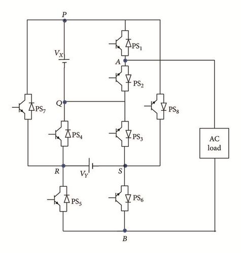
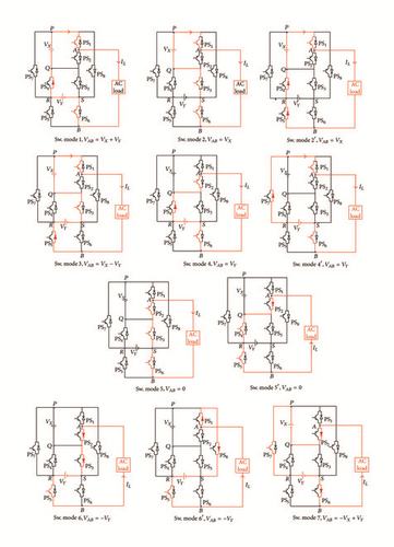
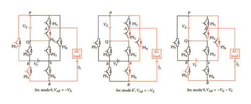
Table 1 shows switching sequence and output voltages generated for both symmetric and asymmetric mode of operation.
| Sw. mode | PS1 | PS2 | PS3 | PS4 | PS5 | PS6 | PS7 | PS8 | Output voltage |
|---|---|---|---|---|---|---|---|---|---|
| 1 | 1 | 0 | 0 | 1 | 0 | 1 | 0 | 0 | VX + VY |
| 2 | 1 | 0 | 1 | 0 | 0 | 1 | 0 | 0 | VX |
| 2′ | 1 | 0 | 0 | 1 | 1 | 0 | 0 | 0 | |
| 3 | 1 | 0 | 1 | 0 | 1 | 0 | 0 | 0 | VX − VY |
| 4 | 0 | 1 | 0 | 1 | 0 | 1 | 0 | 0 | VY |
| 4′ | 1 | 0 | 0 | 0 | 0 | 1 | 1 | 0 | |
| 5 | 0 | 1 | 1 | 0 | 0 | 1 | 0 | 0 | 0 |
| 5′ | 0 | 1 | 0 | 1 | 1 | 0 | 0 | 0 | |
| 6 | 0 | 1 | 1 | 0 | 1 | 0 | 0 | 0 | −VY |
| 6′ | 1 | 0 | 0 | 0 | 1 | 0 | 0 | 1 | |
| 7 | 0 | 1 | 0 | 0 | 0 | 1 | 1 | 0 | −VX + VY |
| 8 | 0 | 1 | 0 | 0 | 1 | 0 | 1 | 0 | −VX |
| 8′ | 0 | 1 | 0 | 0 | 0 | 1 | 0 | 1 | |
| 9 | 0 | 1 | 0 | 0 | 1 | 0 | 0 | 1 | −VX − VY |
2.1. Operation of Basic Block of Proposed Topology
The operation of proposed topology is explained using single phase basic block shown in Figure 1. It consists of two voltage sources VX and VY and eight semiconductor switches. Each switch consists of a MOSFET/IGBT with antiparallel diode and has two operating states. The sequence of operation of all possible states is shown in Figure 2. It is seen that only three switches are conducting in any switching mode. The load is supplied by different voltage levels. According to magnitude of voltage sources selected the same basic block generates five-level, seven-level, or nine-level output voltage as shown in Table 2.
| Sr. number | Output voltage | Symmetric mode | Asymmetric mode | |
|---|---|---|---|---|
VAB for VX = VY = E |
VAB for VX = 2E, VY = E |
VAB for VX = 3E, VY = E |
||
| 1 | VX + VY | 2E | 3E | 4E |
| 2 | VX | E | 2E | 3E |
| 3 | VX − VY | 0 | E | 2E |
| 4 | VY | E | E | E |
| 5 | 0 | 0 | 0 | 0 |
| 6 | −VY | −E | −E | −E |
| 7 | −VX + VY | 0 | −E | −2E |
| 8 | −VX | −E | −2E | −3E |
| 9 | −VX − VY | −2E | −3E | −4E |
3. Generalized Cascaded Circuit Topology

Different combination of dc voltage source magnitudes can be selected for operation of this cascaded circuit. It can enrich performance of multilevel inverter and can also increase the number of levels. Seven different combinations to select magnitude of dc voltage sources are discussed here.
3.1. First Combination (C1)
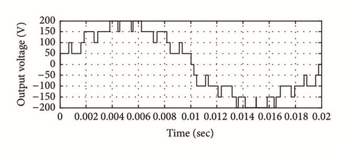
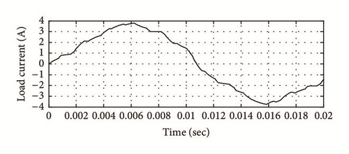
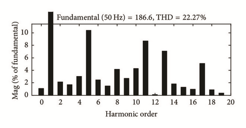
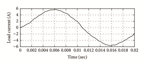
In this arrangement four dc sources of equal magnitudes are used. Figure 4 shows that simulation results for the arrangement with E are equal to 50 V.
3.2. Second Combination (C2)
In this structure four dc sources of two varieties of magnitude and 16 switches generate 13 levels of output voltage with maximum and minimum level of +6E and −6E, respectively. Figure 5 shows simulation results. E is supposed to be 50 V.

3.3. Third Combination (C3)
Output voltage waveform of this 17 level inverter based on this structure is shown in Figure 6. E is supposed to be 50 V.
3.4. Fourth Combination (C4)
In the above equations, Nl, n represent the number of output voltage levels and number of basic blocks used in series.
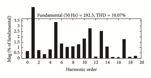
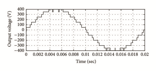
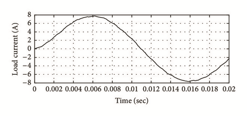
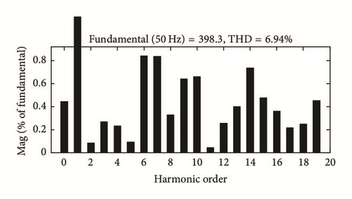
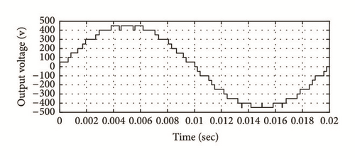
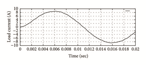
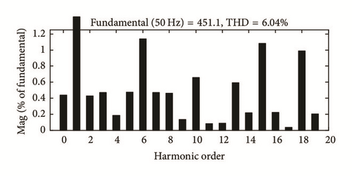
Considering the above, employing four dc sources with three varieties of magnitude and 16 switches, 19 levels of output voltage are obtainable with maximum and minimum level of +9E and −9E, respectively. Figure 7 shows simulation results. E is assumed to be 50 V.
3.5. Fifth Combination (C5)
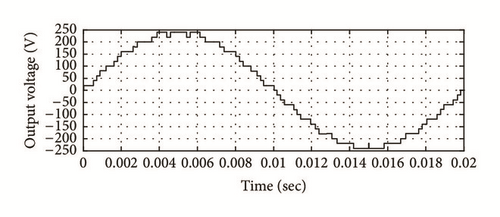
In this structure, using 16 switches, 25 levels of output voltage can be generated. Figure 8 shows simulation results. E is supposed to be 20 V.
3.6. Sixth Combination (C6)
Here, n is number of basic blocks connected in series.
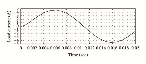
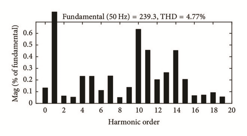
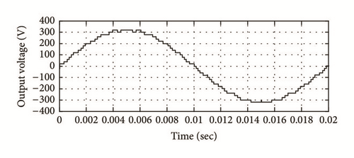
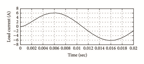
In this case 33 levels of output voltage can be produced with maximum and minimum level of +16E and −16E, respectively. Figure 9 shows simulation results. E is supposed to be 20 V.
3.7. Seventh Combination (C7)
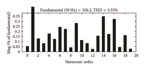
Simulation results for this 49-level multilevel inverter are shown in Figure 10. E is supposed to be 20 V for the instance.
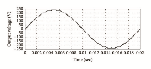
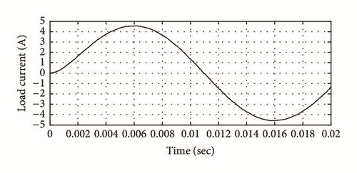
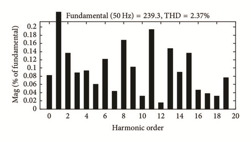
Illustration is carried out using two blocks in series for all the above combinations of cascaded multilevel inverter. From simulation results it is seen that, for combinations one to seven, the number of levels of output voltage increases as 9, 13, 17, 19, 25, 33, and 49. And as the number of levels increases harmonic contents decrease improving its quality.
4. Calculation of Standing Voltage of Switches
To improve performance of multilevel inverter and to increase number of output voltage levels it is possible to select different combinations of dc voltage sources. To choose magnitudes of dc voltage sources seven different combinations are presented here. For these seven combinations magnitude of dc sources, maximum output voltage generated (Vm), number of output voltage levels (Nl), variety in values of dc sources (Nv), and total maximum voltage blocked by switches (Vbt) are calculated and shown in Table 3.
Combination number |
DC voltage source magnitudes | - | Vm | Nl | Nv | Vbt |
|---|---|---|---|---|---|---|
| First (C1) | VX(k) = VY(k) = E | 2E | 2nE | 4n + 1 | 1 | 10nE |
| for k = 1,2, 3, …, n | ||||||
| Second (C2) | VX(k) = 2E, | 3E | 3nE | 6n + 1 | 2 | 16nE |
| VY(k) = E | ||||||
| for k = 1,2, 3, …, n | ||||||
| Third (C3) | VX(k) = 3E, | 4E | 4nE | 8n + 1 | 2 | 22nE |
| VY(k) = E | ||||||
| for k = 1,2, 3, …, n | ||||||
| Fourth (C4) | VX(k) = 2VY(k), | 3 × 2(k−1) × E | 3 × (2n − 1) × E | (3 × 2n+1) − 5 | n + 1 | |
| VY(k) = 2(k−1)E | ||||||
| for k = 1,2, 3, …, n | ||||||
| Fifth (C5) | VX(k) = VY(k) = 5(k−1)E | 2 × 5(k−1) × E | ((5n − 1)/2) × E | 5n | n | |
| for k = 1,2, 3, …, n | ||||||
| Sixth (C6) | VX(k) = 3VY(k), | 4 × 3(k−1) × E | 2 × (3n − 1) × E | (4 × 3n) − 3 | n + 1 | |
| VY(k) = 3(k−1)E | ||||||
| for k = 1,2, 3, …, n | ||||||
| Seventh (C7) | VX(k) = 2 × 7(k−1)E | 3 × 7(k−1) × E | ((7n − 1)/2) × E | 7n | 2n | |
| VY(k) = 7(k−1)E | ||||||
| for k = 1,2, 3, …, n | ||||||
5. Comparison
All the seven combinations are compared with each other. Figure 11 compares number of switches required to generate particular number of output voltage levels. It is seen that sixth and seventh combination (C6 and C7) require less number of switches to generate particular number of output voltage levels.
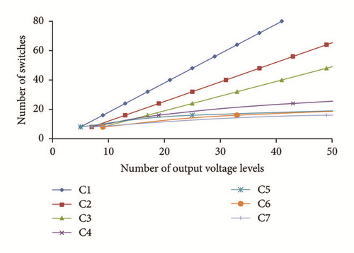
Figure 12 compares number of dc sources required in different combinations. As shown in graph seventh combination (C7) requires minimum number of dc sources and first combination requires maximum number of dc sources to generate particular number of output voltage levels.
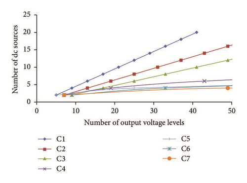
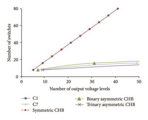
Figure 13 shows comparison among proposed and conventional topologies of CHB. First combination C1 which is symmetric proposed topology and seventh combination C7 which gives best performance among seven combinations are considered for comparison. C1 and symmetric CHB generate the same amount of output voltage levels by using particular number of switches. Therefore, both lines overlap each other. But in C1 to produce suppose 5 levels only 3 switches are conducting at any instant while in symmetric CHB 4 switches are conducing and so on. Means conduction losses are less in C1 as compared to conventional symmetric CHB. C7 requires less number of switches as compared to symmetric CHB and binary asymmetric CHB to generate particular number of output voltage levels. Though the number of switches required in trinary asymmetric CHB is less, the number of conducting switches is more as compared to C7 to generate particular number of output voltage levels. So conduction losses are less in C7.
6. Simulation and Experimental Results
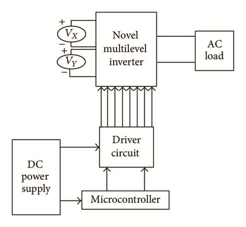
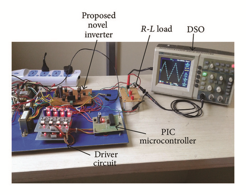
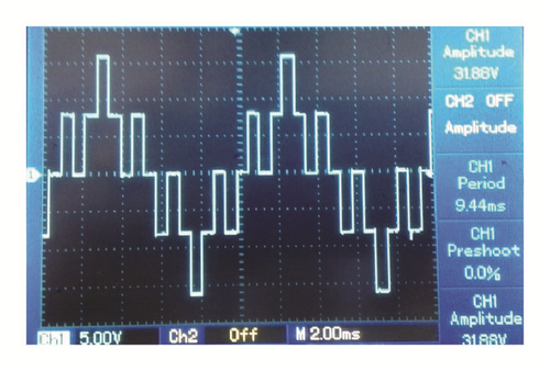
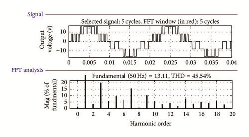
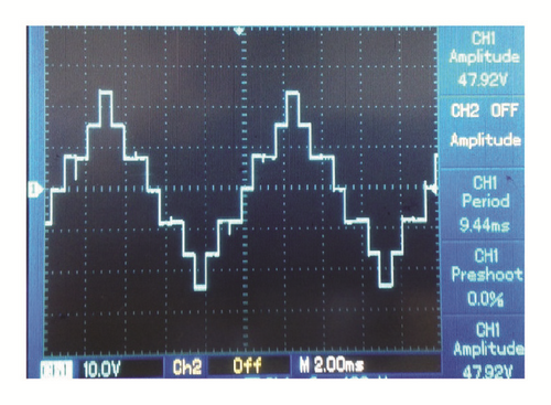
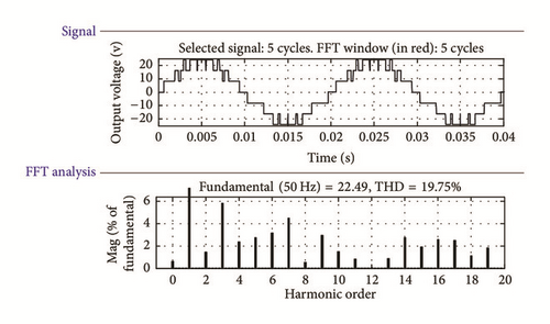
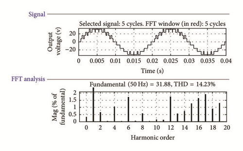
To validate proposed topology shown in Figure 1, the experimental and simulation results are presented for basic unit of single phase inverter operating in symmetric mode (VX = E and VY = E) and asymmetric mode (VX = 2E and VY = E, VX = 3E and VY = E). It generates 5-level, 7-level, and 9-level output voltage as mentioned in Table 2. MOSFETs-IRF840 are used as power switches in the prototype. Microchip’s PIC-16F877A microcontroller is used to provide pulses for the switches. TLP250 optoisolated gate driver is used to provide amplified gate signals to switches as well as provide isolation between power and control circuit. The block diagram is shown in Figure 14(a) and photograph of hardware setup is shown in Figure 14(b). Components used are given in Table 4. Figures 15, 16, and 17 show simulation and experimental results of single phase inverter. It is seen that both results are in line.
| Sr. number | Component used | Specification |
|---|---|---|
| 1 | V X | 8 V, for 5-level output |
| 16 V, for 7-level output | ||
| 24 V, for 9-level output | ||
| 2 | VY | 8 V |
| 3 | PIC microcontroller | 16F877A |
| 4 | Gate driver | TLP250 |
| 5 | MOSFET | IRF840 |
| 6 | Load | R = 50 ohms |
| L = 100 mH |

7. Conclusion
A basic block of novel multilevel inverter topology has been proposed in this paper. Connecting basic blocks in series a cascaded circuit is developed. Seven different combinations to select magnitude of dc voltage sources are introduced. Comparison is carried out among different combinations to find out the best one. From comparison it is seen that C7 requires less number of switches, while C1 needs less variety of magnitude of dc voltage sources.
The main advantage of proposed topology is in increasing as well as getting flexibility in number of output voltage levels by using less number of on-state power switches and dc voltage sources. Simulation results prove the validity of proposed topology and cascaded circuit in producing high voltage containing low value of harmonics. Also, the practicality of basic unit of proposed topology is verified experimentally for the small-scale prototype in the laboratory.
Conflicts of Interest
The authors declare that they have no conflicts of interest.


