A New CDS Structure for High Density FPA with Low Power
Abstract
Being an essential part of infrared readout integrated circuit, correlated double sampling (CDS) circuits play important roles in both depressing reset noise and conditioning integration signals. To adapt applications for focal planes of large format and high density, a new structure of CDS circuit occupying small layout area is proposed, whose power dissipation has been optimized by using MOSFETs in operation of subthreshold region, which leads to 720 nW. Then the noise calculation model is established, based on which the noise analysis has been carried out by the approaches of transfer function and numerical simulations using SIMULINK and Verilog-A. The results are in good agreement, demonstrating the validity of the present noise calculation model. Thermal noise plays a dominant role in the long wave situation while 1/f noise is the majority in the medium wave situation. The total noise of long wave is smaller than medium wave, both of which increase with the integration capacitor and integration time increasing.
1. Introduction
Infrared detectors have a wide range of applications in areas of military, research, and manufacture, whose core part is an infrared focal plane assembly. The assembly mainly consists of two parts: focal plane arrays (FPAs) that function to convert radiation to current signal and readout integrated circuits (ROIC) that are responsible for realization of serial read and processing of signals sampled by the FPA.
Being an essential part of infrared readout integrated circuit, correlated double sampling (CDS) circuits play important roles in both depressing reset noise and conditioning integration signals [1–3]. Applications of focal planes of large format and high density put forward more harsh demand on low power dissipation and small layout area of a ROIC unit cell. Based on the theory that MOSFETs operating in the subthreshold region consume much less dissipation than those in the depletion region, this paper proposed a low power CDS structure that contains only one sampling capacitor, two switches, and two operation amplifiers (OPs), which saves the layout area [4, 5]. Then the noise calculation model is established, based on which noise analysis has been carried out by the approaches of transfer function and numerical simulation using SIMULINK and Verilog-A, whose results are in good agreement.
2. Circuit Design
2.1. Operating Principle
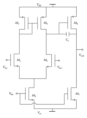
The proposed CDS circuit is shown in Figure 1. It comprises two Ops A1 and A2 that are connected as buffers, a sampling capacitor Csh and two complementary switches S1 and S2. A1 and A2 are standard two stage OPs, which are shown in Figure 2. They can provide high gain in order to reduce the error caused by the transmission process of the signals, in the meanwhile guarantee low noise.
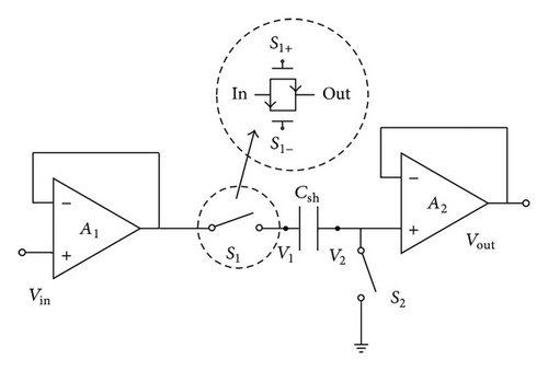
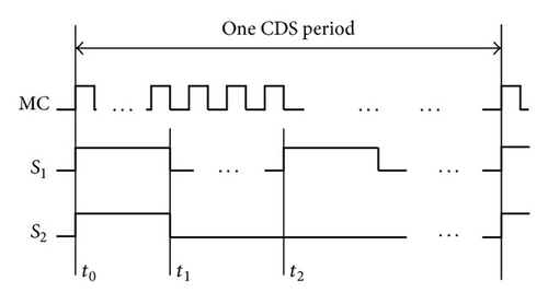
The clock timing waveforms of the CDS circuit are also illustrated in Figure 1. After the integrator resets, S1 and S2 are both switched on at “t0” and the reset voltage of the integrator is coupled on the “V1” node, which is the first sample; then the two switches are off at “t1,” so the charge of Csh remains unchanged until “t2”; after the integration duration, S1 is turned on while S2 remains off at “t2,” and the second sampled signal is stored on “V1” node. Because of the law of conservation of charge, the voltage of “V2” node jumps by the difference value between the two sampling processes, which cuts off the error that resulted by the reset process of the integrator and suppresses low frequency noise. The proposed circuit structure is easy to implement, where using OP provides the conditions that no extra bias voltage is needed. As is known, capacitors occupy the most layout area; thus the design of only one capacitor saves much area. Besides subthreshold technology applied makes the proposed CDS circuit suitable for ROIC unit cells of the large format FPAs.
2.2. Power Optimization
MOSFETs operating in subthreshold region have larger gm-to-channel current ratio than those in saturation region, which implies that subthreshold technology can be applied to optimization power dissipation of analog ICs with the guarantee for sufficient gain [7]. Table 1 is the comparison of the performance for the OPs consisting of MOSFETs working in different regions, where the supply voltages are 0 Volts to 3 Volts. It can be seen that the dissipation of the OP with the design of subthreshold technology succeeds in reducing at least one order of magnitude at the price of tradeoff with frequency character like small SR and GBW.
| Working region | Gain (dB) | GBW (Hz) | SR (V/us) | Power (W) |
|---|---|---|---|---|
| Saturation | 78 | 50.5 M | 10.2 | 622 u |
| Saturation | 72.5 | 1.7 M | 0.62 | 5.5 u |
| Subthreshold | 75.6 | 1.58 M | 0.57 | 720 n |
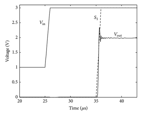
Figure 3 shows the transient response of the proposed CDS circuit with the two OPs A1 and A2 designed by the subthreshold technology, in which the reset voltage is 1 Volt, the output of the integrator is 3 Volts, and S1 is switched on at “t2” After slight oscillation the output of the CDS circuit reaches 2 Volts, which is the integration voltage.
3. Noise Analysis
3.1. Noise Calculation Model
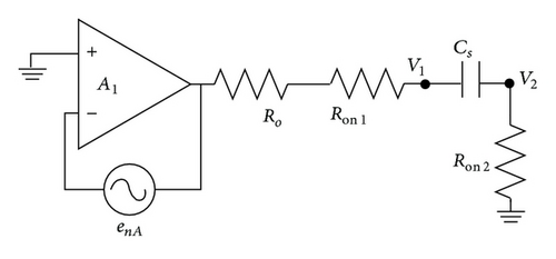
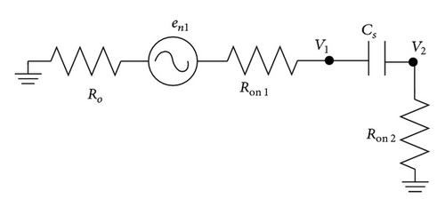
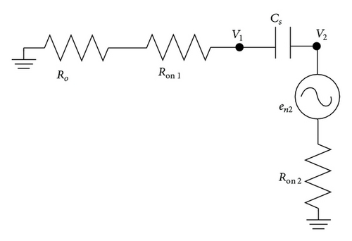
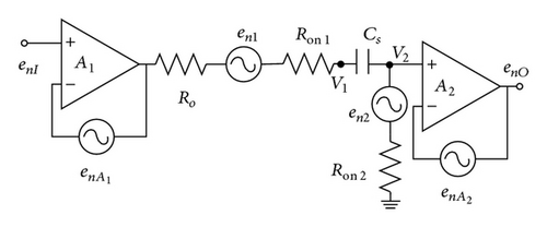
The calculation model of noise for the proposed CDS circuit is illustrated in Figure 4, involving four noise sources, which are from the two OPs and the two switches, respectively. The noise sources of the switches are thermal noise and the noise of the OPs is composed of thermal noise and 1/f noise.
3.2. Noise Calculation
| Ron1, Ron2 | 2.2 kΩ |
| K1e1, K1e2 | 4.0 × 10⁻¹⁷ V2/Hz |
| K2e1, K2e2 | 4.2 × 10⁻¹¹ V2/Hz |
| GBW1, GBW2 | 1.58 MHz |
| Ro | 560 kΩ |
Detectors capable of different wavebands produce a variety of densities of photocurrent, which leads to different integration time needed at certain ability of charge processing. We define Kint = Tint/Cint as the integration factor, determined by the value of photocurrent and output swing of the ROIC. Tint means integration time, that is, the time interval between the two sampling processes of CDS, and Cint is integration capacitor. Figure 5 gives the output noise and its component noise of the proposed CDS circuit as functions of Cint under the situations of applications of long wave and medium wave, respectively. Kint is 50 K for typical long wave and 1 MEG for medium wave. As can be seen, noise increases with Cint increasing for long wave detection, in which 1/f noise has greater growth than thermal noise; when Cint < 2pF, thermal noise dominates. For medium wave situation, owing to the radiation weaker than that for long wave, larger Tint is needed at the same Cint. The fact mentioned above results in longer interval between the two sampling processes of CDS, thus causing inferiority of suppressing 1/f noise. We can see that under medium wave situation 1/f noise is larger than thermal noise and rises with Cint increasing. By comparison of the two situations, we conclude that the noise that CDS circuit brings into the signal chain is larger for medium wave application than that for long wave.
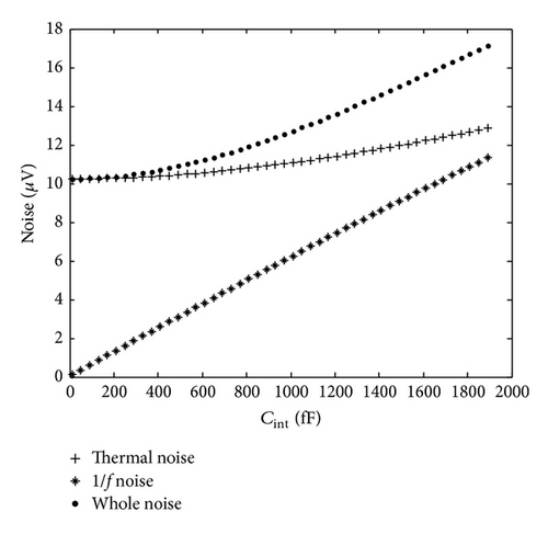
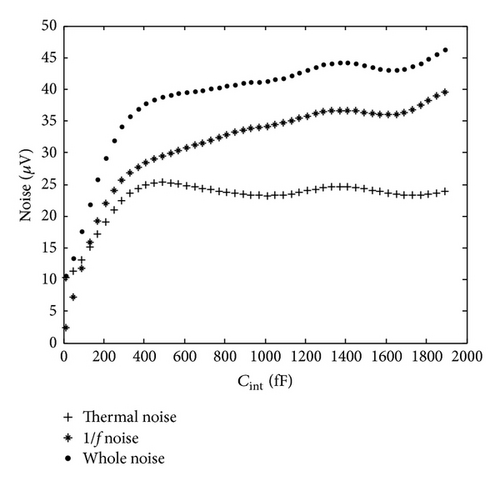
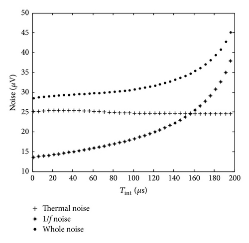
Figure 6 shows the noise varying as functions of Tint at fixed Cint, in which we can see 1/f noise is increasing with Tint increasing; while thermal noise nearly remains the same, the reason can be concluded through analysis that the increasing of Tint results in the increasing of in its low frequency area; thus more noise of low frequency is transmitted to the output node of the CDS circuit.
4. Simulation Experiment
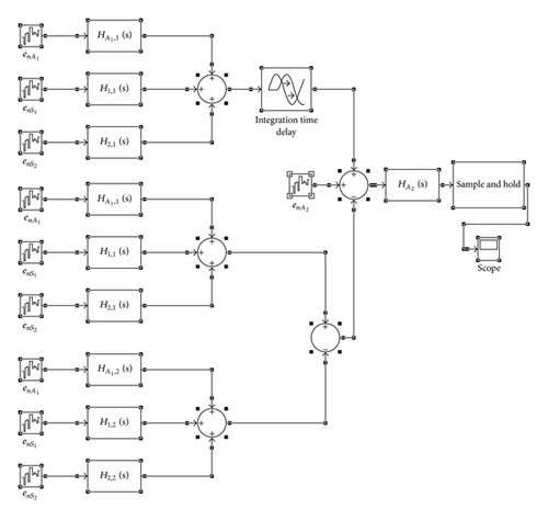
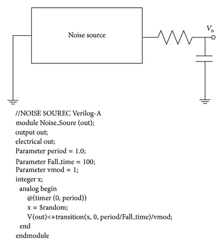
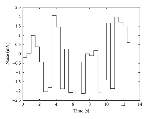
The transient analysis model of the proposed CDS circuit is constructed in SIMULINK, which is shown in Figure 7. Thermal noise can be presented directly using the module in the simulator and 1/f noise is modeled by the approach brought out in [10]. HSPICE provides the possibility to simulate circuit noise in AC response by computing the PSD but cannot give the waveform of noise in transient response directly, whereas we carried out an approach to model time domain noise source using Verilog-A in this paper [11], as is shown in Figure 8(a). The noise is filtered by an RC filter, which settles its bandwidth. The waveform can be seen in Figure 8(b).
At last we averaged the RMS of the output noise from the scope in Figure 7 and output noise obtained by Verilog-A method to compare with those that were calculated by the equations in Section 2, and the unit of noise is uV. The three sets of results, which are given in Table 3, are in good agreement, therefore proving the feasibility of the method of transfer function noise analysis.
| Tint | 100 ns | 1 us | 10 us | 100 us | 150 us | 200 us |
|---|---|---|---|---|---|---|
| Theoretical results | 28.03 | 29.39 | 29.41 | 31.20 | 34.02 | 46.62 |
| SIMULINK results | 27.44 | 28.57 | 28.82 | 30.71 | 34.05 | 47.52 |
| Verilog-A results | 27.19 | 29.11 | 28.23 | 30.26 | 32.80 | 49.57 |
5. Conclusion
For the applications of FPAs of large format and high density, a new structure of CDS circuit is proposed, whose power dissipation has been optimized by subthreshold technology, which leads to 720 nW. Because of using only one sampling capacitor, the proposed CDS circuit occupies small layout area. Then the noise calculation model is established, based on which the noise analysis has been carried out by the approaches of transfer function and numerical simulation using SIMULINK and Verilog-A. The results are in good agreement, demonstrating the validity of the present noise calculation model. Thermal noise plays a dominant role in the long wave situation while 1/f noise is the majority in the medium wave situation. The total noise of long wave is smaller than medium wave, both of which increase with the integration capacitor and integration time increasing.
Conflict of Interests
The authors declare that there is no conflict of interests regarding the publication of this paper.
Acknowledgment
The authors thank the Key Laboratory of Opto-Electronic Information Processing for the continuous supporting of the research on noise of readout integrated circuits.
Appendix
Explanation of (5)
