Butterfly-Inspired 2D Periodic Tapered-Staggered Subwavelength Gratings Designed Based on Finite Difference Time Domain Method
Abstract
The butterfly-inspired 2D periodic tapered-staggered subwavelength gratings were developed mainly using finite difference time domain (FDTD) method, assisted by using focused ion beam (FIB) nanoscale machining or fabrication. The periodic subwavelength structures along the ridges of the designed gratings may change the electric field intensity distribution and weaken the surface reflection. The performance of the designed SiO2 gratings is similar to that of the corresponding Si gratings (the predicted reflectance can be less than around 5% for the bandwidth ranging from 0.15 μm to 1 μm). Further, the antireflection performance of the designed x-unspaced gratings is better than that of the corresponding x-spaced gratings. Based on the FDTD designs and simulated results, the butterfly-inspired grating structure was fabricated on the silicon wafer using FIB milling, reporting the possibility to fabricate these FDTD-designed subwavelength grating structures.
1. Introduction
Nowadays, there is an increasing trend to learn from nature to analyze natural structures and develop bioinspired devices/elements through mimicking or replicating natural structures [1–11]. It has been reported that the moth eyes have inspired the researchers to develop antireflective structured photovoltaic materials and devices (e.g., solar cells) for higher light-to-electricity conversion efficiency [12–18], and the lotus leaves have excited the investigators to design the self-cleaning/hydrophobic structures or surfaces [19, 20]. Like the nanostructures of moth eyes and lotus leaves, the structures of butterfly wings, which may contribute to their own colors [2, 5–10, 21–30], carry the potential to develop new materials, techniques, and devices for different applications.
The reported butterfly-inspired technologies/products consist of the hydrophobic or self-cleaning materials/surfaces [6–8, 21, 22], the high-efficiency solar panels [5, 9, 23, 24], the vapor or gas nanosensors [6, 8, 10, 25], the iridescent ZrO2 photonic crystals [26], the optical beam splitter [27], and the magnetooptic structures [28]. Differently, in this study, the butterfly-inspired newly designed 2D periodic tapered-staggered subwavelength gratings were developed using finite difference time domain (FDTD) simulation method, assisted by using focused ion beam (FIB) nanoscale machining or fabrication (the already achieved grating designs and their antireflection performance were obtained based on FDTD simulation).
2. Materials and Methods
The butterfly species used in this study consisted of the Palm King and the Hebomoia leucippe. The FIB system was used for nanomachining and imaging. The FDTD method was utilized for design and optical performance computation. The designed grating structure was fabricated on the silicon wafer.
3. Structural Analysis for Butterfly Wings Using FIB Nanomachining
The butterfly wings are the translucent and/or pigmented chitin membranes covered with lots of transparent and/or pigmented microscopic light-interacting scales. These microscales may have the function for coloration, waterproofing characteristics (repel water-like roof tiles), and/or solar energy collection (Figure 1). These thin and nanopatterned chitin scales overlap one another, which may allow the dynamic control of light flow and photon interaction by selectively filtering out certain wavelengths through refraction, interference, and/or absorption while reflecting others for visual colorations, subject to the real scale structure and the scale layer distance.
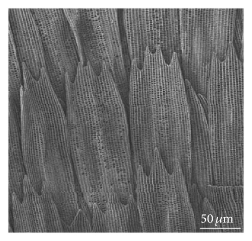
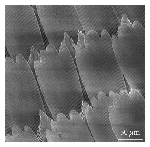
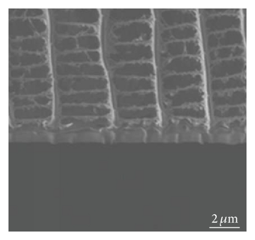
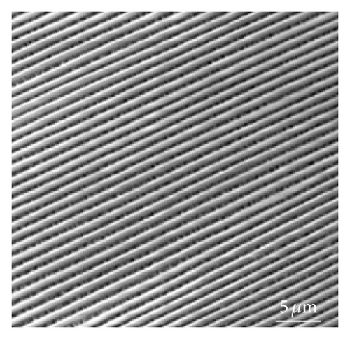
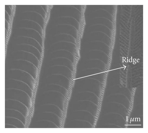
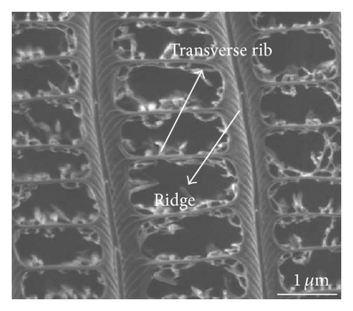
The structures in the scales of the observed butterfly wings are shown in Figures 2 and 3. The general structures in each wing scale are grating-based which consist of the taper- or flute-shaped longitudinal ridges with subwavelength grating substructures and the transverse ribs with/without ovoid pigment granules. The pigment granules on the cross ribs of the wing scales of the Hebomoia leucippe can be removed using FIB, and the exposed structures after FIB nanomachining are shown in Figures 2(a) and 3(b), which appear similar to those of the Palm King (Figure 3(a)) despite the flute-like grating structures shown in Figure 2(b).
4. 2D Periodic Tapered-Staggered Subwavelength Gratings
The inverse-V structures of the black wings of butterfly Ornithoptera goliath may achieve good antireflection property (99% absorption and 1% reflection in visible light spectrum 380–795 nm, the reflectance of the reverse V-type surface is around 1/13 of that in the flat plate). Thus, they show promising antireflection applications for the optical instruments, sensors, thermal detectors, and solar cells [24]. However, as shown in Figure 3, the observed tapered grating ridges have lots of subwavelength periodic grating substructures, whose antireflection performance has not been reported, without mentioning the other functions of these ridge-directional subwavelength periodic grating substructures.
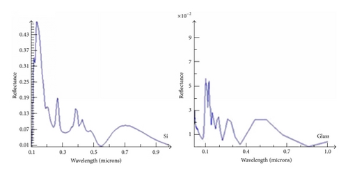
Accordingly, inspired by the nanostructures observed in the scales of the butterfly wings (Figure 3), the 2D periodic tapered-staggered subwavelength gratings were developed. The designed 2D periodic tapered-staggered subwavelength gratings are shown in Figures 4 and 5 (the mimic design of the grating structures of the observed butterfly wings), and the designed grating dimensions are given in Tables 1 and 2. The calculated normal-incident reflectance for the designed gratings at various wavelengths and polarization angles is given in Figures 6−8, where the reference axis for the polarization angles (0° and 90°) is the x-axis.
| a (nm) | b (nm) | c (nm) | d (nm) | e (nm) | h (nm) |
|---|---|---|---|---|---|
| 100 | 200 | 200 | 100 | 100 | 100 |
| a (nm) | b (nm) | c (nm) | d (nm) | h (nm) |
|---|---|---|---|---|
| 50 | 100 | 100 | 50 | 200 |

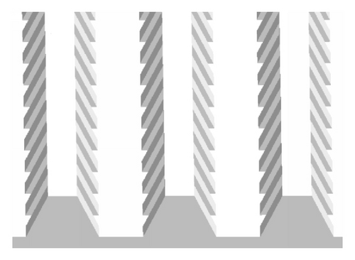
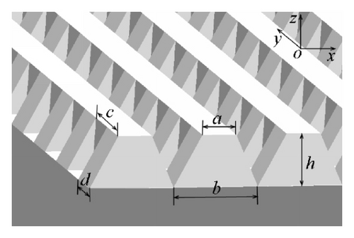
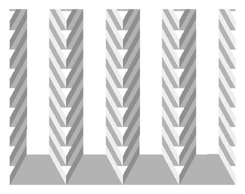
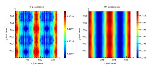
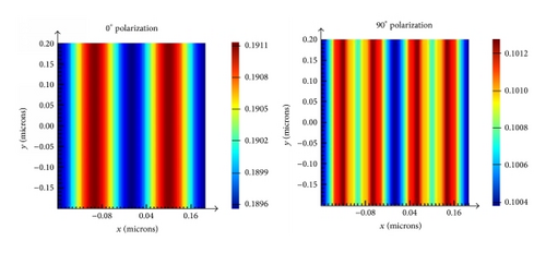
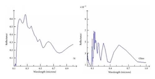
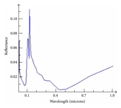
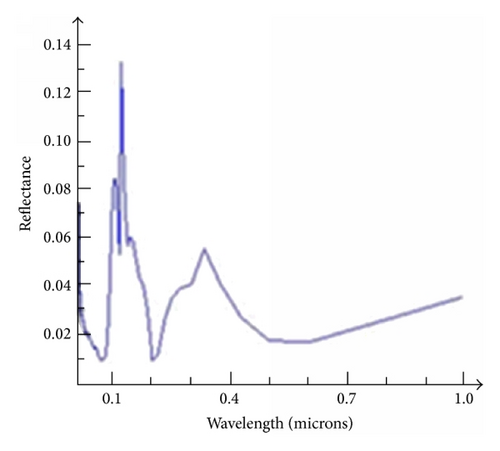
Different from the reflective performance of the general right-angled gratings (geometric dimensions designed: Λ = 200 nm, F = 50%, and h = 200 nm), the periodic subwavelength structures along the ridges of the 2D periodic tapered-staggered gratings may change the electric field intensity distribution (sensitive to light polarization) and weaken the surface reflection (Figure 6). Moreover, the performance of the designed 2D periodic tapered-staggered subwavelength SiO2 gratings is similar to that of the corresponding Si gratings, and the predicted reflectance can be less than around 5% for the bandwidth ranging from 0.15 μm to 1 μm (Figure 7). In addition, as shown in Figures 7 and 8, the antireflection performance of the gratings designed in Figure 5 and Table 2 is better than that of the gratings designed in Figure 4 and Table 1.
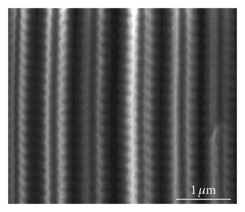
On the basis of the FDTD designs and simulated results, as shown in Figure 9, the butterfly-inspired 2D periodic tapered-staggered subwavelength grating structure was fabricated on the silicon substrate using FIB milling for reporting the possibility to fabricate these FDTD-designed grating structures.
5. Conclusions
The butterfly-inspired 2D periodic tapered-staggered subwavelength gratings were newly developed mainly using the FDTD method. The normal-incident reflectance of the designed gratings at different wavelengths and polarization angles was analyzed. It was shown that the 2D periodic tapered-staggered subwavelength gratings have different reflective performance from those of the general right-angled gratings. Moreover, the periodic subwavelength substructures along the ridges of the designed gratings may change the electric field intensity distribution (sensitive to light polarization) and weaken the surface reflection. Further, the performance of the designed SiO2 gratings is similar to that of the corresponding Si gratings, and the predicted reflectance can be less than around 5% for the bandwidth ranging from 0.15 μm to 1 μm. The antireflection performance of the designed x-unspaced gratings is better than that of the corresponding x-spaced gratings. Based on the FDTD designs and simulated results, the butterfly-inspired 2D periodic tapered-staggered subwavelength grating structure was fabricated on the silicon substrate using FIB milling, reporting the possibility to fabricate these FDTD-designed grating structures.
Conflict of Interests
The authors declare that there is no conflict of interests regarding the publication of this paper.
Acknowledgments
The work is supported by the Research Foundation for Advanced Talents of Jiangsu University under Grant no. 14JDG020, China, and the A*STAR (Agency for Science, Technology and Research) under SERC Grant no. 072 101 0023, Singapore.


