A Study on the Conductivity Variation of Au Coated Conductive Particles in ACF Packaging Process
Abstract
In the ACF packaging process, a bonding force will be applied to the ACF structure. The finite element analysis is used to simulate the ACF packaging process. Material behavior is assumed to be superelastic for resin, viscoelastic for polymer matrix, and elastic-plastic for metal, such as bump, pad, chip, and Au-film. The axis-symmetric model is employed in FEA simulation with time-varying bonding force and operating temperature. In this study, the parameters, including conductive particle diameter, Au-film thickness, and bonding force, are analyzed with nonliner and temperature-dependent material properties. The simulation results indicate that bonding force and operating temperature have strong effects on the formation of concave on Au-film. In addition, surface wrinkle of Au-film will be induced by the bonding force. Both of the concaving and the wrinkling on Au-film will decrease the contact area between the conductive particle and the bump and the contact area between the conductive particle and the pad. Decrease of the contact area means increase of the total resistance for the ACF structure. The results show that the smaller the conductive particle diameter, the smaller the contact area. Generally, increasing the thickness of Au-film will decrease the contact areas, except at the Au-film thickness of 0.05 μm.
1. Introduction
Different interconnect processes are used in flip chip packages, for example, soldering, stud bumping, wire bonding, and other adhesive based processes. The ACF packaging process offers better advantages over other flip chip packaging processes in low operating temperature, high I/O point density, non-lead, environmental friendliness, process simplicity and flexibility, no underfilling, and fine pitch. The Anisotropic Conductive Film (ACF) assembly has also been used widely in the fine pitch flip chip packaging.
However, in difference with traditional soldering, the ACF is generally composed of an adhesive polymer matrix and fine conductive fillers using metallic particles or metal-coated polymer balls. A key point in the development of ACF technology is a tradeoff between the good conduction in z-direction and high insulation in x-y plane. The ACF conductive particles used in COF (Chip-on-Flex) or COG (Chip-on-Glass) packages are usually coated with Au-film on high polymer plastic micro-ball.
The flexible particle can increase the contact area, that is, the decrease of conductive resistance, by deforming the inner plastic microballs. The almost same coefficient of thermal expansion between the conductive microballs and the polymer matrix can reduce the undesired thermal stress disadvantages.
In ACF bonding, the deformable Au coated microballs play the key electrical conduction bridge between the chip and the substrate [1, 2]. Contact resistance of ACF is dominated by the microball contact areas with substrate and chip, respectively. However, the shapes and sizes of contact areas are related to the holding pressure distributed in the polymer matrix. The higher bonding pressure may introduce the larger contact areas; that is, there is a higher conductivity in ACF packaging. In other words, the viscoelastic behavior of the epoxy resin and the deformation of compressed Au coated micro-polymer-balls dominate the conductivity characteristics in ACF packaging process. In 1998, the flow characterization and thermomechanical response in ACF package were first investigated by Dudek et al. [3]. A complex thermal and residual stress distribution was introduced during the bonding and cooling. A power law between the bonding pressure and the electric conductivity was proposed by Shi et al. in 1999 [4]. A simple spring model was employed to explore the mechanical behavior of conductive particles by Chiang et al. [5]. The effect of difference of Young’s modulus and CTE between pad and adhesive polymer matrix on the residual stress and strain distributions in ACF was studied in 2005 [6].
The effects of conductive particle number and size on the electric conductivity have also been investigated numerically and experimentally in several studies [7–11]; pronounced deviations between simulations and experimental data were observed. The misalignment between chip and substrate has also reduced the electric conductivity [12–17]. Although increasing the holding pressure and the concentration of conductive particles may improve the conductivity between chip and pad, but it also may break the insulation between pads. In general, so many parameters, for example, the bump and pad sizes, concentration of conductive particles, material and size of particles, epoxy resin material, and holding pressure in ACF may affect the reliability and contact resistance. In this work, the effects of the Au coating film thickness on the conductive particle and the holding pressure on the conductivity in ACF are investigated.
2. The Electric Contact Resistance of Au Coated Micro-Resin-Balls
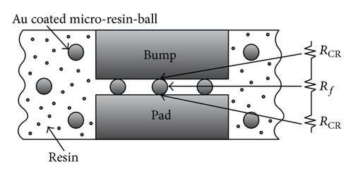
3. The FEM Model for the Au Coated Conductive Microball in ACF
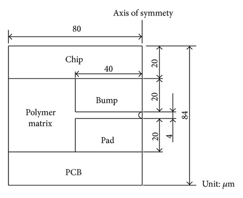
The axial-symmetric model exhibits on Figures 2 and 3 are used to simulate the nonlinear deformation of the Au coated micro-resin-ball during the ACF packaging. In order to improve the conductivity of microball, a thin layer Au has coated outside of the compressed 4 μm diameter mircoball as shown. The same polymer has been used for the ball and matrix to get rid of the undesired thermal stress introduced from the TCE mismatch. The thermal-elastic-plastic finite element model of MARC software was employed in this work. Due to the significant difference between the Young’s moduli and CTE of Au and polymer matrix, the deformation of compressed microball is quite complicate and nonlinear during the ACF packaging. The effects of Au-film thickness and holding pressure on the variation of contact area shape, that is, the electric resistance, are studied in this work.
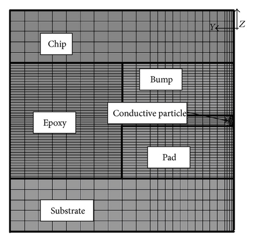
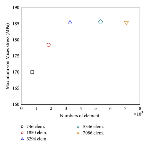
The convergence checks of FEM mesh on the deformation and maximum von Mises stress are illustrated in Figures 4(a) and 4(b). Numerical results reveal that an axial-symmetrical model with 3294 nodes can provide the convergent results. For saving the computing time, an axial-symmetrical model with 3294 quadratic elements is employed.

- (1)
Heating compression: the constant load (50 μN~300 μN) and working temperature (190°C) are applied to compress the conductive microball for 4 seconds as shown in Figures 5 and 6. Under this temperature, the polymer matrix is almost liquidized and does not endure any pressure in this period.
- (2)
Unloading and cooling: the constant load and the temperature are released linearly in the period of 4–8 seconds. After removing the load, the restored force of conductive microball is equivalent to the residual tensile force of the polymer. The magnitude of spring back force introduced by the compressed microball is dependent a number of factors, for example, the curing pressure, the microball size, and the thickness of coated gold film.
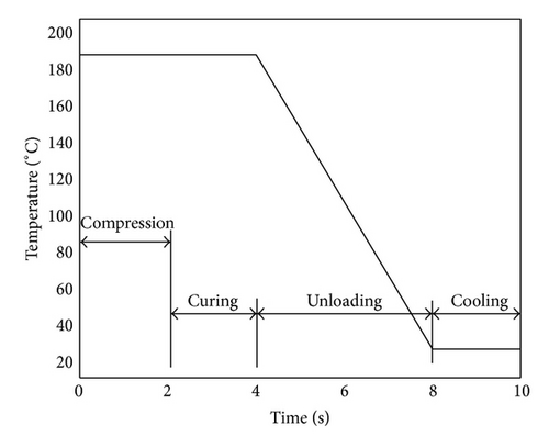
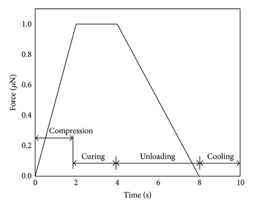
Since the curing temperature (190°C) is much lower than the melting temperature of chip bump and substrate pad materials, the elastic behavior with constant material properties is assumed in this study. The temperature dependent superelastic and viscoelastic material models are assumed for the conductive particle resin and the polymer matrix. Table 1 listed the properties of components involved in the ACF. The friction coefficient between conductive particle and pad is 0.3.
| Material | E [MPa] | ν | CTE (ppm/°C) | σy [MPa] | Constitutive equation |
|---|---|---|---|---|---|
| Chip (Si) | 128000 | 0.30 | 2.7 | — | Elastic |
| PCB (Flex) | 4000 | 0.30 | 20 | — | Elastic |
| Ni-based bump and pad |
|
|
|
405 | Elastic-plastic |
| Polymer matrix |
|
|
|
— | Elastic |
|
|
|
|
— | Elastic |
| Au film | 77000 | 0.30 | 14.2 | 170 | Elastic-plastic |
4. Numerical Results and Discussion
As noted, the shapes and sizes of contact areas between the deformed microball and the bump and the pad dominated the electric resistance in ACF packaging. In general, the flat contact areas are observed. However, in some particular case, a concave deform of the contact area has been observed. For example, the 4 μm diameter with the 0.05 μm gold film coating under a constant 100 μN load force/each microball may have a concave contact area after the heat curing process. This concave deformed shape of the compressed microball, as shown in Figure 7, makes a void near the center. An annular type contact area is observed in this case. The area between the radii Ro and Ri is the contacted area, and the circular area in the radius Ri is a noncontact void. Figure 8 shows the variation of radii Ro and Ri during the heat curing process. The distance between the radii Ro and Ri at 8 seconds indicates the final size of contact region.
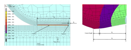
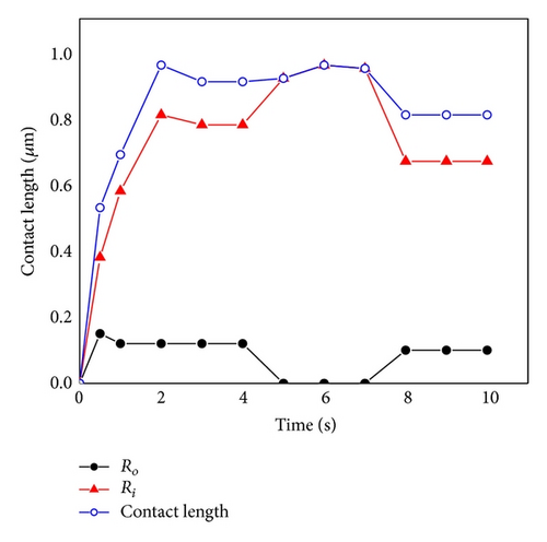
Figure 9 shows the variation of contact radii Ro and Ri of the 4 μm diameter microball (with a 0.05 μm thickness Au coating) under different curing loads on each microball. Results indicate that the concave deformation will disappear when the curing load on each ball is greater than 250 μN. Similar simulations have been applied to 4 μm diameter microball with different thickness Au coatings (0.05 μm, 0.075 μm, 0.1 μm, 0.125 μm, 0.2 μm, and 0.3 μm). The effect of curing load (50 μN, 100 μN, 150 μN, 200 μN, 250 μN, 300 μN, and 350 μN for each ball) on the variation of contact area has also been simulated and studied.
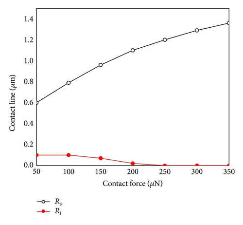
In the hot pressuring step, increasing the bonding force will enlarge the size of the concave. The concave deformation of the loaded microball may reduce the contact area and increase the electric resistance. This loading introduced concave deformation on the Au film will remain with the same shape and size during the curing procedure. Due to the expansion of the polymer matrix in the unloading and package cooling steps, the concave shrinks. Figure 8 shows the size variation of the concave in the manufacturing process. Table 2 lists the numerical results for different cases with a 4 μm diameter of the conductive particle. It is found that the deformation of the concave has an influence on the contact area. According to (1), the variation of the contact area changes the total conductive resistance of the ACF structure. In Table 2, the concaving zone is marked by an oval inside which the value of Ri is not zero. It is observed in Table 2 that increasing the Au-film thickness will shrink the concave. For the Au-film thickness of 0.05 μm case, Figure 9 shows the variation of the contact length versus bonding force. It shows that increasing the bonding force can minimize the size of the concave.
| Particle diameter (4 μm) | ||||||
|---|---|---|---|---|---|---|
| Load force (μN) | Au-film thickness (μm) | |||||
| 0.05 | 0.075 | 0.1 | 0.15 | 0.2 | 0.3 | |
| 50 | ||||||
| Ro | 0.529 | 0.661 | 0.612 | 0.564 | 0.472 | 0.429 |
| Ri | 0.096 | 0 | 0 | 0 | 0 | 0 |
| 100 | ||||||
| Ro | 0.788 | 0.892 | 0.818 | 0.746 | 0.611 | 0.569 |
| Ri | 0.096 | 0 | 0 | 0 | 0 | 0 |
| 150 | ||||||
| Ro | 0.953 | 1.077 | 1.001 | 0.949 | 0.711 | 0.706 |
| Ri | 0.072 | 0 | 0 | 0 | 0 | 0 |
| 200 | ||||||
| Ro | 1.096 | 1.193 | 1.139 | 1.085 | 0.877 | 0.789 |
| Ri | 0.024 | 0 | 0 | 0 | 0 | 0 |
| 250 | ||||||
| Ro | 1.190 | 1.309 | 1.256 | 1.200 | 1.050 | 0.843 |
| Ri | 0 | 0 | 0 | 0 | 0 | 0 |
| 300 | ||||||
| Ro | 1.287 | 1.380 | 1.349 | 1.293 | 1.138 | 0.967 |
| Ri | 0 | 0 | 0 | 0 | 0 | 0 |
| 350 | ||||||
| Ro | 1.359 | 1.451 | 1.419 | 1.388 | 1.278 | 1.103 |
| Ri | 0 | 0 | 0 | 0 | 0 | 0 |
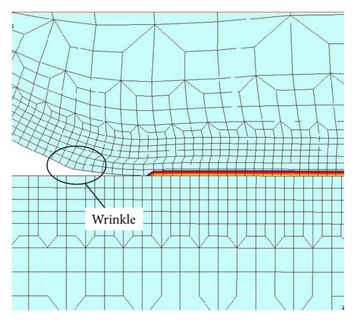
A wrinkle deformation near the contact surface skirt was also observed for the microball with a 0.05 μm Au coated film, as shown in Figure 10. The wrinkle deformation may decrease the contact area, that is, increase the electric resistance. When the load force is larger, the wrinkle deformation is more obvious.
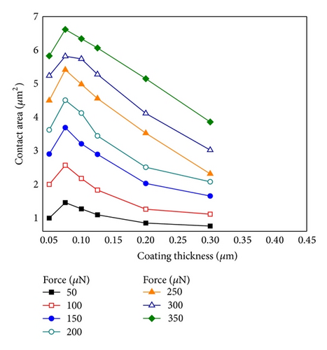
Numerical results in Figure 11 indicate that the contact area size is dependent on the Au-film thickness and the curing load on each microball. The maximum contact area always occurs for the microball with an Au-film thickness of 0.075 μm. An optimum 6.6 μm2 contact area, that is, about 36 micro-ohm, is simulated for a 4 μm microball with a 0.075 μm Au coated film under the curing load of 350 μN/microball. Results also show the decrease of contact area introduced from the wrinkle deformation for the ball with an Au-film thickness less than 0.05 μm.
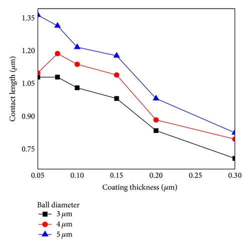
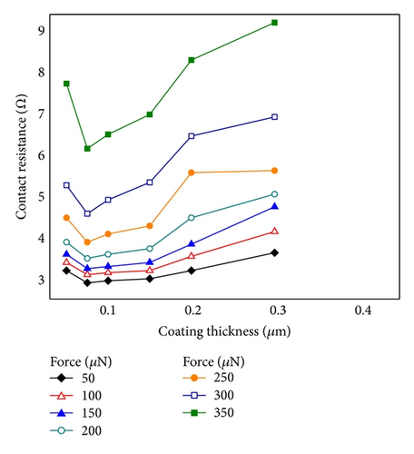
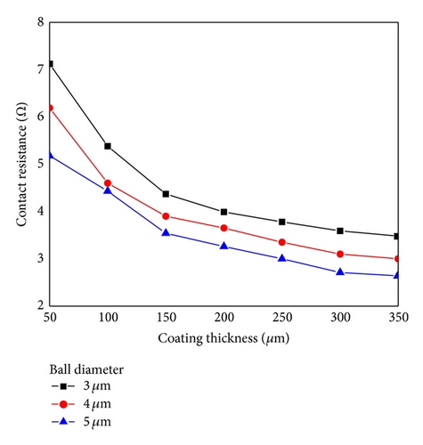
The variation of the contact length versus Au-film thickness is shown in Figure 12 for different bonding forces; the deformation of the conductive particle reduces as the Au-film thickness increases. In addition, the contact area approaches a small value as the contact length reduces. The same result is observed as the particle diameter increases. Hence, substituting the contact length in (1), the relationship between the Au-film thickness and the total resistance can be analyzed. Following the results of Figure 12, the corresponding total resistance of the ACF structure is shown in Figure 13. The total resistance decreases as the bonding force increases as shown. Generally, the total resistance increases as the Au-film thickness increases. However, at the Au-film thickness of 0.05 μm, the value of the total resistance rises unexpectedly as compared to the 0.075 μm case. As shown in Figure 14, the total resistance increases as the particle diameter decreases. As the Au-film thickness increases, it shows that the total resistance reduces.
5. Conclusions
In this work, the effects of curing load and Au coating film thickness of microball on the electric conductance in ACF packaging have been studied by employing a proposed thermal-elastic-plastic FEM model. Numerical results indicate that the surface buckling and local winkle deformations may be introduced from the compressed Au film coated on the microball during curing process. These concave shape buckling and winkle deformations may reduce the contact area and decrease the conductivity significantly as the Au coating thickness is less than 0.05 μm. The simulated results also reveal that the contact area is quite sensitive to the curing load in packaging. The best electric conductance in ACF packaging occurs for the cases with an Au thickness of 0.075 μm and curing load on each ball is greater than 250 µN.
Conflict of Interests
The authors declare that there is no conflict of interests regarding the publication of this paper.


