Gallium Nitride Electrical Characteristics Extraction and Uniformity Sorting
Abstract
This study examined the output electrical characteristics—current-voltage (I-V) output, threshold voltage, and parasitic capacitance—of novel gallium nitride (GaN) power transistors. Experimental measurements revealed that both enhanced- and depletion-mode GaN field-effect transistors (FETs) containing different components of identical specifications yielded varied turn-off impedance; hence, the FET quality was inconsistent. Establishing standardized electrical measurements can provide necessary information for designers, and measuring transistor electrical characteristics establishes its equivalent-circuit model for circuit simulations. Moreover, high power output requires multiple parallel power transistors, and sorting the difference between similar electrical characteristics is critical in a power system. An isolated gate driver detection method is proposed for sorting the uniformity from the option of the turn-off characteristic. In addition, an equivalent-circuit model for GaN FETs is established on the basis of the measured electrical characteristics and verified experimentally.
1. Introduction
Metal-oxide-semiconductor field-effect transistors (MOSFETs) have been widely used over the past 30 years. As silicon approaches its performance limits, wide-bandgap semiconductors, such as gallium nitride (GaN) and silicon carbide (SiC), are emerging technologies that can supersede silicon MOSFETs as next-generation power transistors. Novel wide-band III-nitride semiconductor materials are being rapidly developed because of their unique properties, such as high electron mobility, saturation velocity, sheet carrier concentration at heterojunction interfaces, and breakdown voltages [1, 2]. These properties make III-nitrides feasible for high-power, high-temperature applications. Compared with SiC, GaN has low turn-on and switching losses and is less expensive. In addition, GaN wafers are produced by numerous manufacturers, thus negating any monopoly concerns. Furthermore, GaN has been widely used in light-emitting diodes and wireless applications. GaN power FETs are suitable for high-voltage, high-current, and motor-control applications as well as for industrial automation systems and automotive electronics [3–5].
Because both the commercially enhanced-mode (E-mode) and depletion-mode (D-mode) GaN FETs manufactured by National Chiao Tung University (NCTU) [6, 7] are relatively new types of power transistors, few related studies are available in the literature. In addition, few manufacturers discuss them because commercial applications are not yet prevalent. The electrical characteristics of commercially manufactured power transistors differ because of the differences in cutting, wiring, wire bonding materials and diameters, and packaging. Before using such power transistors in circuit applications, their electrical characteristics must be extracted and sorted to match similar electrical properties in circuit designs. Unfortunately, extracting similar electrical properties is time-consuming and expensive. Thus, rapid and easy extraction of the electrical characteristics of GaN FETs to sort similar electrical properties is essential.
Moreover, GaN FETs and the design of their gate drivers are relatively new. When using GaN FET power transistors in circuit applications, their unique electrical properties must be considered: (1) no intrinsic body diode [8–10], (2) low gate-to-source voltage limits [9, 10], (3) full-conduction voltage of the gate and uncommon power supply voltage (e.g., 7 V, 8 V) [11–13], and (4) low threshold voltage [9, 10, 12, 13]. The following properties are applicable to bridge-leg architecture power transistors: (1) floating source of the high-side power switch [14, 15] and (2) faulty turn-on [9, 15]. Therefore, GaN-FET-based power transistors require appropriate gate drive circuits and methods to prevent overload. Although numerous studies have examined these properties, none have focused on the turn-off characteristic.
This paper first reports the output electrical characteristics of novel GaN power transistors and standardized electrical measurements to provide necessary information for designers. Second, an isolated gate driver detection method is proposed for sorting. Finally, this paper presents a simple and accurate equivalent-circuit model of GaN FETs for circuit simulations, established on the basis of the measured electrical characteristics and verified experimentally.
2. Materials and Methods
2.1. Measurement of GaN Electrical Characteristics
On the basis of MOSFET and GaN-FET datasheets, the following characteristics were used in this study: (1) breakdown voltage 200 V, rated current 9 A, on-resistance 0.4 Ω, and E-mode MOSFET [16]; (2) breakdown voltage 500 V, rated current 6 A, on-resistance 0.5 Ω, and D-mode MOSFET [17]; (3) breakdown voltage 200 V, rated current 12 A, on-resistance 25 mΩ, and E-mode GaN FET [18]; and (4) D-mode GaN FET manufactured in the laboratory as testing devices. The electrical characteristics measured were ID-VD characteristics, threshold voltage, and parasitic capacitance.
2.1.1. ID-VD Characteristic Curve
ID-VD curve measurements detect the maximum output current of the power transistor when the gate voltage VGS is applied as the full-conduction voltage, and the full-conduction on-state resistance is applied between the drain and source (RDS(ON)). The characteristic curve reveals the linear and saturation regions of the circuit, where the device can operate properly. According to the test circuit in [19], the output characteristics are drain current ID versus drain-source voltage VDS measured under different gate voltages VGS ranging from the gate turn-off to full-on voltage at intervals of 1 V. The VGS range of the E- and D-mode MOSFET is 0 to 12 V and −12 to 0 V, respectively, the VGS range of the E-mode GaN FET is 0 to 5 V, and that of the D-mode GaN FET manufactured by NCTU is −5 to 0 V. Drain voltage generally uses a pulse mode input, which prevents excessive heat that affects the output characteristics. According to the datasheets, test pulse properties for E- and D-mode MOSFETs and E-mode GaN-FETs are a pulse width of 300 μs and a duty cycle (duty) ≦ 2% [16–18]. In this study, a test pulse width of 300 μs, pulse period of 300 ms, and duty cycle of 0.1% were used to measure the ID-VD curve characteristics of the four aforementioned power transistors.
2.1.2. Threshold Voltage
Threshold voltage (VTH) is the minimum gate bias required to turn the device on and produce a drain current specified in the datasheet. In the threshold voltage measurement circuit for E-mode power transistors, the drain and gate terminals of the power transistors are shorted (VDS = VGS) [16]. The voltage to the gate terminal is gradually increased from the turn-off voltage Voff (0 V) until the measured current equals the specified drain current. For D-mode power transistors, the drain terminal is connected to a fixed DC voltage source. Similar to the test procedure for E-mode transistors, the voltage to the gate terminal of the D-mode transistor is gradually increased from Voff (−5 V) and changes in its drain current ID are observed. As specified in the datasheet [17], a DC voltage of 25 V is applied to the drain terminal of D-mode MOSFETs. D-mode GaN FETs, which applying to drain terminal’s DC voltage value refer to ID-VD characteristic curve while the drain voltage attains the saturation region under the power transistor, are fully opened (VGS = 0 V). In this study, laboratory-manufactured D-mode GaN FET saturation voltage was set to the voltage measured from the ID-VD characteristic curve. The conduction threshold current of E- and D-mode MOSFET is 250 μA [16, 17] and that of E-mode GaN-FET is 3 mA [18]. The laboratory-manufactured D-mode GaN FET has no datasheet for referencing its conduction threshold current. Therefore, to obtain the gate terminal input voltage VGS at which the drain current ID increases instantaneously, the experimental measurements of the drain current ID are transformed logarithmically [20]. The VGS thus obtained is considered the threshold voltage VTH.
2.1.3. Parasitic Capacitance
A power device analyzer/curve tracer [21] was used to measure the capacitance because it supports the measurement of the three nonlinear capacitances: CGD, CDS, and CGS. Figure 1 depicts the CGD, CDS, and CGS measurement circuits, respectively. A multiple frequency capacitance measurement unit with four ports (Hp, Hc, Lp, and Lc) was used for capacitance measurements. Hp and Hc were shorted together (hereafter, CMH), and Lp and Lc were shorted together (hereafter, CML). The CMH outputs an AC test signal through the circuit under test, which is detected by the CML. The CMH operates in the 100 kHz–1 MHz AC frequency range. As specified in the MOSFET and E-mode GaN-FET datasheets, CGS is measured at 100 kHz, and CDS and CGS are measured at 1 MHz; the oscillation level is 30 mV for all measurements. The CML receiving port potential is equivalent to the ground terminal.

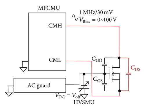

The parasitic capacitance CGD is measured using the circuit shown in Figure 1(a). The AC test signal is output from the CMH to the drain terminal, the source terminal is connected to a high-voltage source/monitor unit (HVSMU), and the source terminal grounds the AC signal to the AC guard. Therefore, the AC test signal from CDS to the source terminal is grounded by the AC guard, preventing the signals from being received by the source terminal through the CGS path. When measuring the parasitic capacitance CGD, the HVSMU should provide a Voff DC bias relative to the CML gate terminal, and the power transistor should be kept off. Both the enhanced MOSFET and E-mode GaN-FET power transistor have the same Voff (0 V), whereas that of the D-mode MOSFET power transistor is −12 V. However, the ID-VD curve revealed that the tested D-mode MOSFET turns off at −5 V. Therefore, in this study, −5 V was used as the Voff for the D-mode MOSFET power transistor. The Voff of D-mode GaN FET is −5 V. Because the source terminal has a bias voltage, −Voff, the CMH should apply an AC bias voltage in the range Voff to 100 − Voff to drain the terminal. Therefore, the bias VDS voltage of measurement can range from 0 to 100 V.
The parasitic capacitance CDS is measured using the circuit shown in Figure 1(b). The circuit is similar to that used to measure CGD; the only difference is that the gate terminal was changed to the source terminal to connect the CML. The CMH outputs an AC test signal to the drain terminal and receives an AC test signal from the CML by connecting CML to the source of the device under test. The gate terminal grounds the AC guard to prevent the AC test signals from being received by the source terminal through the CGD and CGS paths. To ensure that the power transistor remains off during the measurement, the DC voltage Voff is applied to the gate terminal. The CMH gradually increases the AC bias voltage from 0 to 100 V; therefore, the parasitic capacitance measurement CDS is in the VDS voltage range of 0–100 V.
The parasitic capacitance CGS is measured using the circuit shown in Figure 1(c). The CMH outputs an AC test signal to the gate terminal, and the CML receives the signal by connecting to the source terminal. Because the CMH has a Voff bias, the power transistor is kept off. To prevent the signals from being received by the source terminal through the CGD and CDS paths, the drain terminal is grounded to the AC guard. The HVSMU provides DC voltage in the range of 0–100 V; therefore, parasitic capacitance CGS is measured at different VDS voltages in the range of 0–100 V.
2.2. Mechanism of Isolated Gate Drive Detection
2.2.1. Conventional Gate Drive
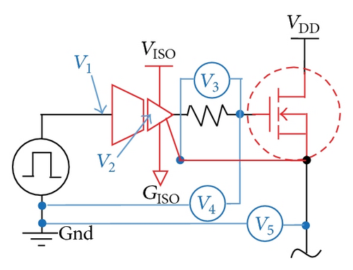
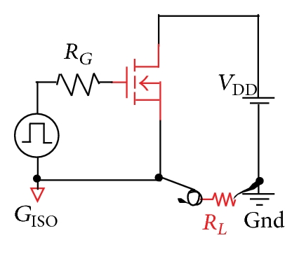
Conventional power transistor gate drives use gate drive integrated circuit (IC) architecture. When used in half- and full-bridge-leg drive topologies, gate drives typically use an optical coupling IC to form an isolated floating-supply gate drive circuit architecture. Isolated gate drive circuit architecture consists of fast optical coupling IC, gate driver IC, and auxiliary supply voltage, as shown in Figure 2. The gate drive voltage for the E-mode GaN FET gate-to-source voltage is VISO − GISO, and the VGS for D-mode GaN FET gate drive voltage is −VISO to GISO. The difference between the gate drive circuits for E- and D-mode GaN FETs is that the input supply voltages for the isolated gate driver amplifier are (+VISO) − (GISO) and (GISO) − (−VISO), respectively. The external gate drive signals of the isolated gate drive circuit for the E-mode GaN FET is [0 to +VISO] relative to the ground (Gnd). Through the fast optical coupling IC, the signal is isolated and converted to [0 to +VISO] relative to GISO. Finally, the isolated signal is amplified through the gate driver IC to drive the E-mode GaN FET. Similarly, the gate drive circuit for D-mode GaN FET is isolated to produce the gate signal [−VISO − GISO] relative to GISO to drive the FET.
2.2.2. Isolated Gate Drive Detection
The isolated gate drive signal waveform can be measured by an oscilloscope to distinguish the waveforms of the turn-off impedance RDS(off) when GaN FETs are in the turn-off state. The proposed detection method is a relatively simple screening method to sort similar electrical characteristics of GaN FETs; by observing the switching waveforms, external stray capacitance in the circuit boards and internal parasitic capacitance in the transistors can be detected. The simple and accurate GaN FET model established on the basis of the measured electrical characteristics can be verified through experimental measurements of the isolated gate drive signal waveforms.
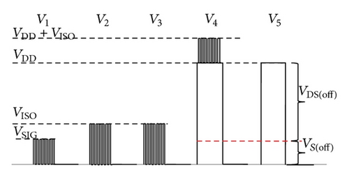
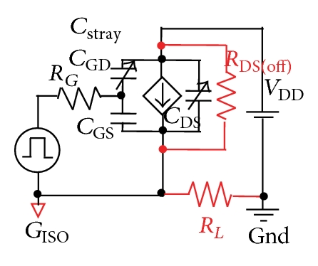
The proposed isolated gate drive detection circuit is illustrated in Figure 2, and the drive signal for the E-mode GaN FET is shown in Figure 3. Voltages V1, V4, and V5 were measured relative to the Gnd; V2 and V3 were measured relative to the isolated supply ground GISO. The drain terminal of the E-mode GaN FET test circuit connects to the power supply voltage VDD relative to the Gnd. When the gate-to-source voltage of the E-mode GaN FET is VISO, it turns on and shorts the drain and source terminals. Ideally, the source terminal voltage relative to the Gnd should be promoted to VDD. The source terminal of the GaN FET and the isolated power source terminal GISO are connected, indirectly causing GISO and GaN FET Gnd to turn on and off; therefore, GISO has a relative floating voltage of VDD. When the gate terminal voltage of the GaN FET relative to the source terminal voltage is VISO, the E-mode GaN FET turns on, the isolated power supply ground GISO relative to the Gnd is VDD, and the voltage between the GaN FET gate terminal and the Gnd is VDD + VISO. When the gate terminal voltage relative to the source terminal is 0 V, the E-mode GaN FET turns off, the gate and source terminals are open, and GISO and Gnd are 0. Because the GaN FET turns off, the drain terminal voltage VDD no longer offers voltage to GISO. The floating voltage VDD discharges through circuit stray capacitance Cstray and load resistance RL. Therefore, GISO floating voltage discharges from VDD at the speed of the resistor-capacitor time constant until the next pulse width modulation (PWM) signal to the gate-to-source voltage is VISO, which turns the GaN FET on again. When the drain terminal voltage VDD is supplied to GISO, the parasitic capacitance CISS can be recharged to VDD + VISO. The higher the PWM drive signal frequency entering the gate terminal, the more stable the GISO in maintaining VDD. When the PWM signal is no longer sent to the gate terminal and the GaN FET remains off for a sufficient period, VDD discharges to 0 V through circuit stray capacitance Cstray [22] and load resistance RL, as shown in Figure 2 (V5). Concurrently, Gnd drops to 0 V. Compared with the turn-off impedance of Si MOSFETs, the turn-off impedance RDS(off) of the GaN FET is low. Therefore, the leakage current offers a load resistance RL to produce voltage VS(off). The turn-off impedance RDS(off) of the GaN FET can be obtained by observing the VS(off) variance.
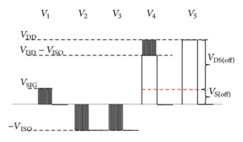
The D-mode GaN FET signal is depicted in Figure 4. When the gate-to-source terminal voltage of the D-mode GaN FET is 0 V, because it is typically turned on, its drain and source terminals are short. In this case, the source-to-ground Gnd voltage should be increased to the power supply voltage VDD, and the GaN FET gate-to-ground Gnd voltage should be VDD. When the gate-to-source terminal voltage is −VISO, the transistor turns off. Concurrently, the gate-to-ground Gnd becomes VDD − VISO. The GISO voltage VDD discharges through the circuit stray capacitance Cstray [22] and the load resistance RL, as shown in Figure 2 (V5), until the next PWM to the gate-to-source terminal voltage is 0 V, which turns the GaN FET on again. The drain terminal voltage VDD provides voltage to GISO. When the gate terminal PWM signal ceases and the GaN FET remains off for a sufficient period, the gate-to-ground Gnd voltage discharges through the circuit stray capacitance and resistance to 0 V. The condition of the D-mode GaN FET is the same as that of the E-mode GaN FET. The turn-off impedance RDS(off) of D-mode GaN FET is smaller than that of Si MOSFET; therefore, the leakage current offers a load resistance RL to produce voltage VS(off). The relationship between the turn-off impedance RDS(off), leakage current, and voltage VS(off) is discussed later.
2.2.3. Isolated Gate Driver Circuit Model
3. Results and Discussion
3.1. ID-VD Characteristic Curve
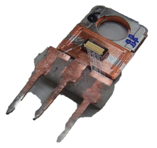
E- and D-mode GaN FET devices under test are shown in Figure 6. The tested D-mode GaN FET chip is 80 mm in size and is packaged in the TO-3P form. Figure 7 depicts the measured ID-VD characteristics of the four power transistors. Solid lines represent the waveforms specified in the datasheets, dotted lines represent the measured waveforms, and solid lines with circles represent the SPICE-simulated waveforms.

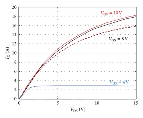
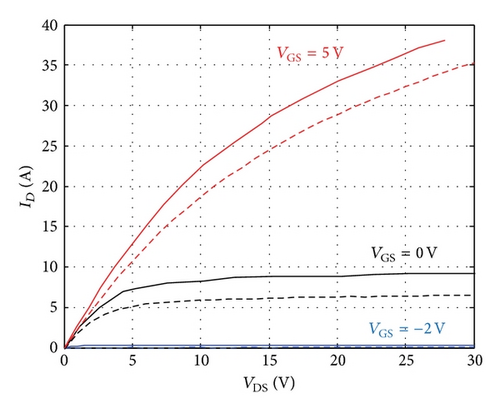
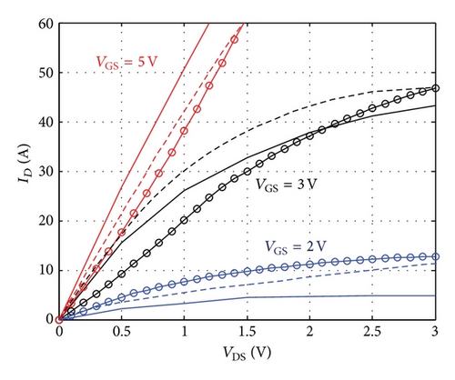
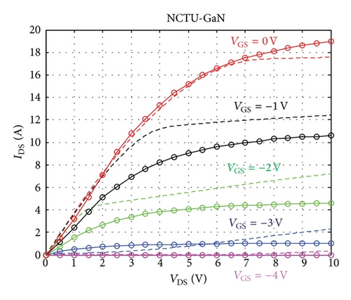
The measured ID-VD characteristics of the E- and D-mode MOSFET waveforms are similar to those specified in the datasheet. The on-resistance RDS(ON) at a specific turn-on gate voltage VGS and drain current IDS can be extracted directly from the output characteristic curves.
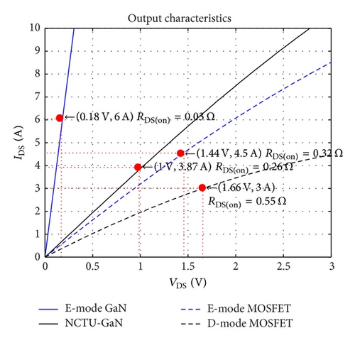
Figure 8 plots the RDS(ON) of the four power transistors. In the enhanced MOSFET, RDS(ON) at VGS = 10 V, VDS = 1.44 V, and IDS = 4.5 A is approximately 1.44/4.5 = 0.32 Ω, which is under the maximum value specified in the datasheet (0.4 Ω). In the D-mode MOSFET, RDS(ON) at VGS = 0 V, VDS = 1.66 V, and IDS = 3 A is approximately 1.66/3 = 0.55 Ω, which is close to the value specified in the datasheet (0.5 Ω). Although the D-mode MOSFET VGS is 0 V, it conducts current but not at full conduction. When VGS is 5 V, VDS is 30 V and the output current ID is 35 A. When VGS is −2 V, the power transistor turns off and the output current ID is close to zero. GaN FET output characteristic variation is considerably large compared with that of the MOSFET. The output current value exhibits drift phenomena in different E-mode GaN FET samples when the inputs VGS and VDS are the same. The experimental results show that the linear region of the on-resistance RON is approximately 0.025–0.03 Ω. When VGS is 5 V and the average output current ID is 6 A, the average voltage VDS is 0.18 V; therefore, the average on-state resistance RON is 0.18/6 = 0.03 Ω, which exceeds the datasheet value of 0.025 Ω. The D-mode GaN FET on-resistance RON is approximately 0.25–0.30 Ω. When VGS is 0 V and VDS is 1 V, ID is 3.87 A; therefore, RON is 1/3.87 = 0.26 Ω.
Equations (5a) and (5b) are used to establish the current source model of a transistor. The output voltage VDS of the E-mode GaN FET is increased from 0 to 3 V at intervals of 0.1 V, and the gate input voltage is increased from 0 to 5 V at intervals of 1 V; the output voltage VDS of the D-mode GaN FET is increased from 0 to 10 V at intervals of 0.5 V, and the gate voltage is increased from −5 to 0 V at intervals of 1 V.
The waveforms are shown in Figures 7(c) and 7(d) as solid lines with circles; the simulated characteristics are similar to the measured characteristics (dashed lines). Drain current IDS (Y-axis) at a particular voltage VDS (X-axis) can be obtained from the simulated waveform. In addition to the on-resistance RON characteristics, the saturation voltage of the D-mode GaN FETs exhibits variance. The experimental results show that the average saturation voltage is at VDS = 7 V and that the maximum saturation current is between 16 and 18 A. The conduction resistance RDS(ON) of the D-mode GaN FET is 0.26 Ω, which is smaller than those of the two MOSFET power transistor (0.32 and 0.55 Ω) but much larger than that of the E-mode GaN FET (0.03 Ω). In the future, RDS(ON) of the D-mode GaN FET can be improved using internal or external parallel methods [6, 7]; therefore, uniform performance should be sorted.
3.2. Threshold Voltage
The measured threshold voltage VTH is plotted in Figure 9. The conduction threshold current of the MOSFET power transistor is defined as 250 μA. From the experimental results of the enhanced MOSFET, the threshold voltage VTH is 3.21 V, which is in the range specified in the datasheet (2–4 V). Furthermore, the conduction threshold current of the D-mode MOSFET is 250 μA; therefore, the gate threshold voltage VTH is −2.98 V, which is in the range specified in the datasheet (−4 to −2 V). From the information in the manual, E-mode GaN FET conduction threshold current is defined as 3 mA.
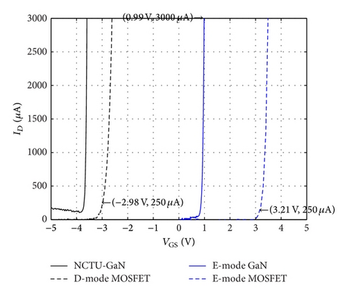
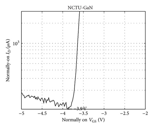
In Figure 9(a), when the output current of the E-mode GaN FET is 3000 μA, the gate threshold voltage VTH is 1 V, which is in the range specified in the datasheet (0.7–2.5 V). The output current ID of the D-mode GaN FET is plotted logarithmically in Figure 9(b). Near VGS = −3.9 V, the output current ID rises rapidly. Hence, this VGS voltage is defined as the threshold voltage of the D-mode GaN FET. The threshold voltage VTH of the E-mode GaN FET is much lower than that of the MOSFET.
3.3. Parasitic Capacitance
The datasheet provides power transistor parasitic capacitance characteristics, including the input capacitance (CISS), output capacitance (COSS), and transpose capacitance (CRSS = CGD), where CISS = CGS + CGD, COSS = CGD + CDS, and CRSS = CGD. Figure 10 plots the measured parasitic capacitance values of the four power transistors. From Figure 10(a), for the E-mode MOSFET, at VGS = 0 V and the bias voltage VDS = 25 V, the parasitic capacitances CISS, COSS, and CRSS are 553.8, 91.5, and 27.3 pF, respectively, which are close to the datasheet values (540 (typ.), 90 (typ.), and 35 pF (typ.), resp.). From Figure 10(b), the E-mode GaN FET, at VGS = 0 V, and a bias voltage VDS = 100 V, parasitic capacitances CISS, COSS, and CRSS are 473.7, 301, and 16.7 pF, respectively, which are close to the datasheet values (540 (max.), 350 (max.), and 12 pF (max.)). From Figure 10(b), the D-mode MOSFET, at VGS = −10 V, and a bias voltage VDS = 25 V, parasitic capacitances CISS, COSS, and CRSS are 2361.7, 243.7, and 61.7 pF, respectively, and CISS is under the value specified in the datasheet (2800 pF (typ.)), whereas COSS and CRSS are close to the datasheet values (255 (typ.), 64 pF (typ.)). For the E-mode GaN FET, at VGS = 0 V and VDS = 100 V, parasitic capacitances CISS, COSS, CRSS are 473.7, 301, and 16.7 pF, respectively, which are close to the datasheet values (540 (max.), 350 (max.), and 12 pF (max.)). For the D-mode GaN FET, at VGS = −5 V and VDS = 50 V, the parasitic capacitances CISS, COSS, and CRSS are 72.7, 64.4, and 10.2 pF, respectively. Comparison of datasheet and measured characteristics are listed in Table 1, and Table 2 lists the important I-V and capacitance model parameters for E- and D-mode used in this study.
| Parameter | Symbol | Test conditions | E-mode GaN FET Value |
D-mode GaN FET Value |
Unit |
|---|---|---|---|---|---|
| On-state resistance | RDS(ON) |
|
~25 m (max.)/30 m | — | Ω |
|
— | —/0.26 | |||
| Gate threshold voltage | VTH |
|
0.99 | — | V |
|
— | −3.9 | |||
| Input capacitance | CISS |
|
|
|
pF |
| Output capacitance | COSS |
|
|
|
pF |
| Reverse transfer capacitance | CRSS |
|
|
|
pF |
| Before slash: datasheet; after slash: measured | |||||
| Symbol | GaN FETs model parameter | ||
|---|---|---|---|
| Parameter | E-mode | D-mode | |
| KP | Transconductance parameter (A/V2) | 24 | 2.1 |
| VTO | Zero-bias threshold voltage | 1 V | −3.9 V |
| δ | Fitting parameter to adjust the curvature | 0.4 | 0.6 |
| CGS | External gate to source capacitance (nF) | 0.45 | 0.06 |
| CGD | External gate to drain capacitance | ||
| CGD0 (nF) | 0.1 | 0.02 | |
| VJ (V) | 0.66 | 0.75 | |
| m | 0.39 | 0.14 | |
| CDS | External drain to source capacitance | ||
| CDS0 (nF) | 0.89 | 0.07 | |
| VJ (V) | 0.4 | 0.35 | |
| m | 0.22 | 0.05 | |
| Cstray | Stray capacitance in the circuit (nF) | 2 | 2 |
| RL | Voltage probe resistance (Ω) | 10 M | 1 M |
| RDS(off) | GaN FET turn-off resistance (Ω) | 7.647 M | 904.8 k |
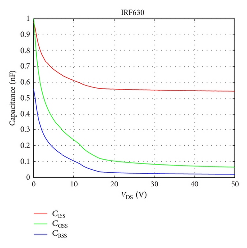
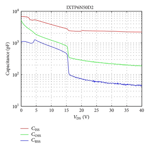
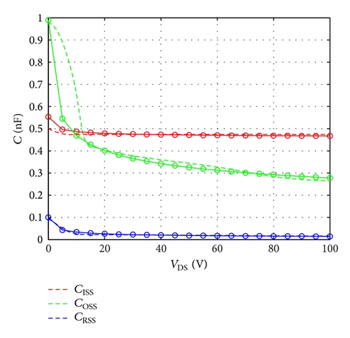
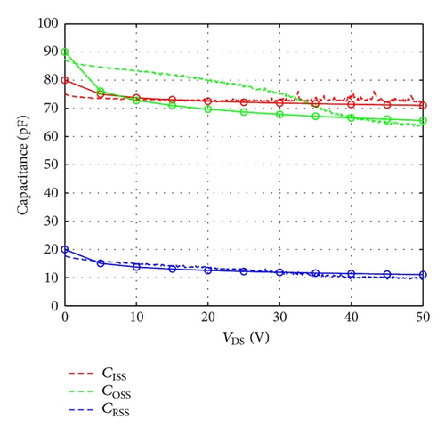
According to (6a) and (6b), the parameters listed in Table 2 are used. The relationships CISS = CGS + CGD, COSS = CGD + CDS, and CRSS = CGD are used. Plots of CISS, COSS, and CRSS are shown in Figures 10(c) and 10(d). The simulated and experimental curves are similar.
3.4. Isolated Gate Drive Detection
A turn-off voltage of 0 V is used for the E-mode GaN FET; therefore, the full-conduction voltage is limited to 5.5 V. For the D-mode GaN FET, the used turn-off voltage is −5 V, and full-conduction voltage is limited to 2 V. Hence, the driving voltage for the E-mode GaN FET gate-to-source voltage is set to 0−5 V; in other words, VISO is set to 5 V, and the D-mode GaN FET gate source driving voltage is set to −5 to 0 V. At driving voltages of 0–5 V and −5 to 0 V, the E- and D-mode MOSFET waveforms can be contrasted. Regardless of the MOSFET mode, the voltage probe was used to measure the voltage between the gate terminal and the ground terminal. The E-mode MOSFET waveforms are the same as the ideal isolated gate drive circuit detection signal, as depicted in Figures 3 and 4; the gate voltage when turned on is +29 V and decreases to 0 V when turned off (Figure 11(a)). The D-mode MOSFET gate voltage waveform is +24 V, which decreases to 0 when turned off (Figure 11(b)). When measuring the E-mode GaN FET, the gate voltage is +29 V when turned on, but a difference in voltage level exists between the gate and the ground. The large change in the voltage level is in the 0–24 V range, as shown in Figure 12(a). D-mode GaN FETs exhibit the same phenomenon, as shown in Figure 12(b). The differences are caused by the turn-off impedance RDS(off). The larger the turn-off impedance is, the smaller the leakage current is; the across voltage VS(off) is small, and the difference between source-to-ground voltage value is close to 0. Conversely, when the turn-off impedance is small, the leakage current is large, and the source-to-ground voltage approaches +24 V. Therefore, the turn-off ability of GaN FETs can indirectly screen device uniformity. Moreover, the impedance value can be quantified.
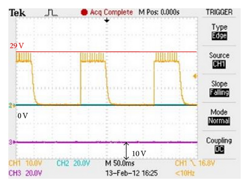

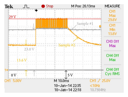
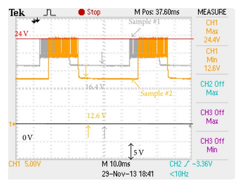
When VGS = 5 V, the E-mode GaN FET turns on. The gate-to-ground voltage is +29 V; when VGS = 0 V, the E-mode GaN FET turns off, which is equivalent to the turn-off resistance RDS(off); the voltage probe resistance is RL. When the Kirchhoff circuit laws are applied, the power supply voltage VDD through RDS(off) and RL generate the leakage drain current IDSS. Through the isolated gate drive circuit architecture, the voltage probe resistance RL is 10 MΩ and power supply voltage VDD is 24 V. The VS(off) values for the two modes are 13.6 V and 23.0 V, as shown in Figure 12(a). Substituting these values into (2), RDS(off) is obtained as 7.647 and 0.435 MΩ. Using a digital multimeter in series with the source terminal and the voltage probes (RL) to measure the GaN FET device during the turn-off state, the leakage currents IDSS are obtained as 1.340 and 2.365 μA. By substituting VS(off) in (1a), leakage currents IDSS are obtained as 1.36 and 2.30 μA, which are similar to the measured values.
Next, the gate-to-ground voltage waveform of the D-mode GaN FET is measured. When VGS is 0 V, the D-mode GaN FET drain and source conducts and shorts, and the source terminal voltage is +24 V. Because VGS = 0 V, the gate terminal voltage is +24 V; when VGS = −5 V, the GaN FET is off, because the resistance of the D-mode GaN FET RDS(off) is not large enough; therefore, leakage current flows, and the source terminal voltage relative to ground cannot be reduced to 0 V. Next, the turn-off voltage of the D-mode GaN FET is measured using the 10 MΩ voltage probe; the value is always 19 V. The turn-off impedance RDS(off) is much lower than 10 MΩ; therefore, the voltage probe is adjusted to 1 MΩ to repeat the experiments. VS(off) is in the 0–19 V range. RDS(off) and voltage probe RL = 1 MΩ divide the voltage, assuming that the probe is measured as VS(off) voltage. From (1a), (1b), and (2), the leakage current IDSS and turn-off impedance RDS(off) can be obtained.
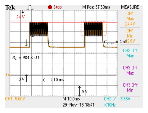
The waveform variability of the D-mode GaN FET is similar to that of the E-mode GaN FET, as shown in Figure 12(b). The D-mode GaN FET under a voltage probe RL = 1 MΩ varies in the 16–20 V range. From (2), RDS(off) of the D-mode GaN FET is 463.4 kΩ when VS(off) is 16.4 V and 904.8 kΩ when VS(off) is 12.6 V. However, when VS(off) exceeds 24 − 5 = 19 V, the turn-off impedance is insufficient and the transistor does not turn off.
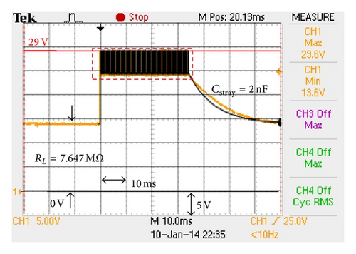
In the E-mode GaN FET, the threshold voltage VTH of the output characteristic curve I-V model parameter is set to 1 V and KP is set to 24. An external capacitor is used as listed in Table 2. In the isolated gate driver circuit architecture, the voltage probe resistance RL = 10 MΩ, power supply voltage VDD = 24 V, and measuring voltage VS(off) = 13.6 V. From (2), RDS(off) impedance is derived as 7.647 MΩ when VS(off) is 13.6 V; therefore, when E-mode GaN FET turns off, the drain-to-source RDS(off) is equivalent to a 7.647 MΩ resistor. RL is the internal voltage probe resistance, which is 10 MΩ at 10x magnification. In the D-mode GaN FET, the threshold voltage VTH of its I-V output characteristic curve model is −3.9 V and KP is 2.1. The external capacitor is used as parasitic capacitance. The turn-off impedance RDS(off) of the experimental device using the 10x magnification voltage probe is much lower than 10 MΩ. Hence, a 1x (1 MΩ) probe is used to measure (RL = 1 MΩ); the power supply voltage VDD = 24 V and the measured VS(off) voltage = 12.6 V. From (2), when VS(off) voltage is 12.6 V, RDS(off) is 904.8 kΩ. The equivalent turn-off resistance RDS(off) between the drain-source is equivalent to 904.8 kΩ.
SPICE circuits are established through the equivalent model described in Figure 5. The gate resistor uses 100 Ω RG, and the E-mode GaN FET gate terminal wave signal VGS voltage is 0–5 V, whereas the D-mode GaN FET VGS is −5 to 0 V. Gate pulse width, period, and frequency of the PWM signal are 100 μs, 500 μs, and 2 kHz, respectively. The numerical analysis software predicts that the gate drive circuit board has external drain-source stray capacitance Cstray and that the actual measurements of waveform segments have a slower falling slope. Because of stray capacitance Cstray parallel to drain-to-source and gate-to-drain, the turn-off VGS slope falls slowly in the waveform. The estimates of the stray capacitance Cstray value are 2 nF. The GaN FET gate detection simulation parameters are shown in Table 2.
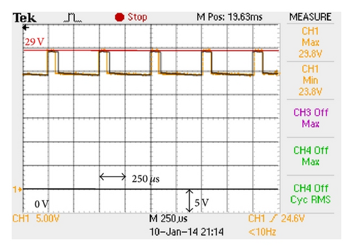
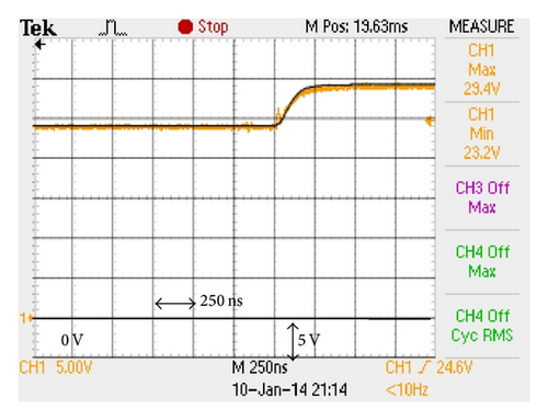
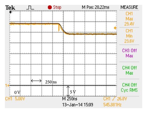
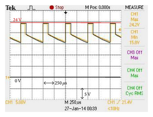
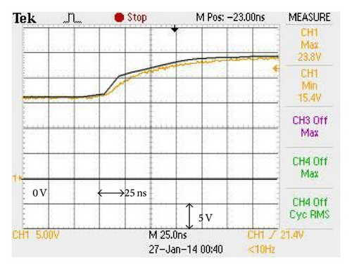
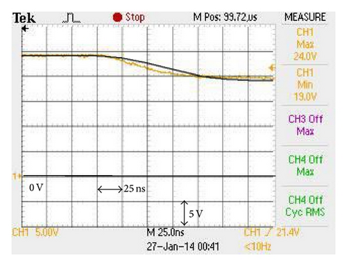
Figures 13 and 14 present the E- and D-mode GaN FET gate detection simulation circuit waveform as shown in black line and measurement waveform as shown in orange line superimposing they are matching each other. When the isolated gate detection circuit stops sending the PWM signal to the gate terminal and GaN FET is set to close long enough, the falling slope waveform segment of the discharge through circuit stray capacitance Cstray and load resistor RL from +24 V floating voltage discharge to the voltage VS(off) is in accordance with the measurement. The influence of the parasitic capacitance of the input capacitance CISS on VGS voltage switching waveform can be observed by enlarging the VGS voltage signal timeline, as shown in the inset of Figures 13(a), 13(b) and 14(a), 14(b); the enlarged VGS voltage signal charge and discharge waveforms are shown in Figures 13(c), 13(d), 14(c), and 14(d). The simulation and experimental gate voltage waveforms of the charge and discharge match perfectly.
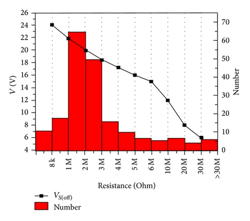
The results of the screening and recording of the turn-off voltage VS(off) and the corresponding RDS(off) of the E-mode GaN FET voltages are shown in Figure 15. The off-resistance of E-mode GaN FETs is larger than 1 MΩ, whereas those of D-mode GaN FETs are approximately in the 0.5–1.5 MΩ range.
4. Conclusions
The on-resistance RDS(ON) of E-mode GaN FET and NCTU D-mode GaN FET is 0.025–0.03 Ω and 0.25–0.3 Ω; both of these values are lower than that of MOSFET. Nevertheless, NCTU’s D-mode GaN FET can be further improved using the parallel method to reduce on-resistance. Regarding parasitic capacitance, the CRSS of the E-mode GaN FET is far lower than that of the enhanced MOSFET; a smaller CRSS capacitance value indicates that the Miller plain area is relatively short and that the switching time is shorter. Compared with the turn-off resistance of different samples, the electrical characteristics of each MOSFET device are highly consistent, whereas those of GaN FET exhibit less uniformity. GaN FETs are currently under development, and the electrical characteristics of each component are relatively unstable; the variability is larger than that in MOSFET. This study established a standardized electrical measurement procedure that provides necessary information for designers. In addition, a simple and accurate GaN FET model was established on the basis of the measured electrical characteristics. The simulation waveforms can be used to obtain information on GaN FET’s internal parasitic capacitance, turn-off impedance RDS(off), and stray capacitance Cstray in the inverter circuit board. The proposed GaN FET isolated gate drive circuit screening method by RDS(off) detection provides a simple uniformity sorting method. The results show that the higher the off-state voltage VS(off) is, the smaller the turn-off voltage VDS(off) is; in other words, the device has a lower RDS(off). The leakage current in GaN devices is much larger than that in MOSFET devices in the turn-off state. The off-resistance of MOSFET is generally larger than 10 MΩ. By contrast, the off-resistance of E-mode GaN FETs is larger than 1 MΩ, whereas those of D-mode GaN FETs are approximately in the 0.5–1.5 MΩ range. Devices with the same off-state voltage VS(off) perform similarly. Moreover, the larger the turn-off resistance RDS(off) is, the closer the characteristics are to those specified in the datasheet.
Conflict of Interests
The authors declare that there is no conflict of interests regarding the publication of this paper.
Acknowledgments
This work was supported by the CSIST Project CSIST-0101-V108(104), Taiwan. The authors would like to thank Professor Edward Yi Chang of NCTU for supporting GaN devices, Professor Stone Cheng of NCTU for supporting package technology, and National Nano Device Laboratories, Hsinchu, Taiwan, for their very helpful suggestions and technical support.


