Plasmon-Enhanced Photoluminescence of an Amorphous Silicon Quantum Dot Light-Emitting Device by Localized Surface Plasmon Polaritons in Ag/SiOx:a-Si QDs/Ag Sandwich Nanostructures
Abstract
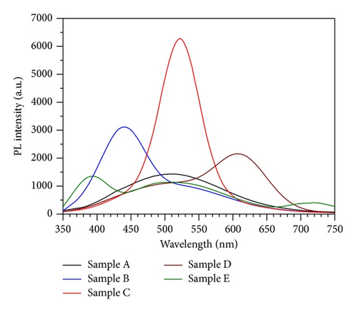
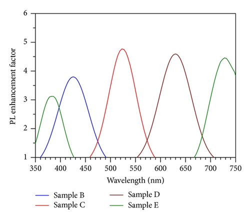
We investigated experimentally the plasmon-enhanced photoluminescence of the amorphous silicon quantum dots (a-Si QDs) light-emitting devices (LEDs) with the Ag/SiOx:a-Si QDs/Ag sandwich nanostructures, through the coupling between the a-Si QDs and localized surface plasmons polaritons (LSPPs) mode, by tuning a one-dimensional (1D) Ag grating on the top. The coupling of surface plasmons at the top and bottom Ag/SiOx:a-Si QDs interfaces resulted in the localized surface plasmon polaritons (LSPPs) confined underneath the Ag lines, which exhibit the Fabry-Pérot resonance. From the Raman spectrum, it proves the existence of a-Si QDs embedded in Si-rich SiOx film (SiOx:a-Si QDs) at a low annealing temperature (300°C) to prevent the possible diffusion of Ag atoms from Ag film. The photoluminescence (PL) spectra of a-Si QDs can be precisely tuned by a 1D Ag grating with different pitches and Ag line widths were investigated. An optimized Ag grating structure, with 500 nm pitch and 125 nm Ag line width, was found to achieve up to 4.8-fold PL enhancement at 526 nm and 2.46-fold PL integrated intensity compared to the a-Si QDs LEDs without Ag grating structure, due to the strong a-Si QDs-LSPPs coupling.
1. Introduction
2. Experiments
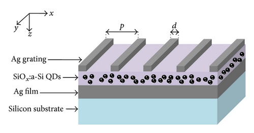
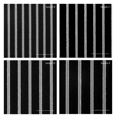
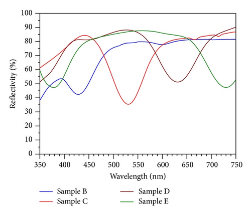
The fabrication process of the trilayer Ag/SiOx:a-Si QDs/Ag sandwich nanostructures is described as follows. Silicon substrate was first coated with a 100 nm-thick Ag film using thermal evaporation. Then, the 100 nm-thick Si-rich SiOx (SRO, x < 2) film was deposited on the Ag film by using plasma enhanced chemical vapor deposition (PECVD) system at the pressure of 67 Pa with nitrogen-diluted 5% SiH4 and N2O as the reactant gas sources. The flow rate of N2O gas was maintained at 30 sccm and the SiH4/N2O flow rate ratio of 5.53 : 1. The sample was heated to 350°C and the radio frequency power was kept at 30 W during the SRO film growth. After the deposition, the SRO film was annealed at 300°C for 1 hr in a quartz furnace with flowing N2 gas, to form a SiOx:a-Si QDs film. Then, a 1D periodic Ag grating was fabricated on the top of SiOx:a-Si QDs film using electron-beam (e-beam) lithography (Elionix ELS-7500) and liftoff process. First, a 300 nm-thick positive-type e-beam resist (Nippon Zeon ZEP-520A) is spun on the top of sample followed by the subsequent e-beam lithography to define the grating pattern with the pitch p and line width d. The duty cycle (d/p) of Ag grating is fixed at 25%. Second, a 50 nm-thick Ag film is deposited onto the patterned e-beam resist and the Ag grating is fabricated by liftoff process in an exclusive remover (Nippon Zeon ZDMAC). Figure 1 shows the schematic representation of device with Ag/SiOx:a-Si QDs/Ag sandwich nanostructures. The structural parameters of devices (samples A–E) are listed in Table 1. Scanning electron microscopy (SEM) images of Ag gratings (samples B–E) are shown in Figure 2. The room-temperature photoluminescence (PL) spectra were acquired under the excitation from a He-Cd laser operating at λexcitation = 325 nm and with an average power of 50 mW. The PL intensity within 350 nm and 750 nm was recorded using a monochromator (CVI DK240) in conjunction with a photomultiplier (Hamamatsu R928) and a digital multimeter (HP 34401A). The reflection spectra were measured in an optical microscope consisting of a monochromator (Horiba Jobin Yvon iHR 320) and a broadband halogen lamp as a white light source incident through a 20x objective (NA = 0.75) to the normal of the metal surface (z-axis). And the reflected light was collected with the same objective. The refraction index of Si-rich SiOx film was determined by an ellipsometer (JA Woollam M-2000DI). The thickness of each Ag film and SiOx:a-Si QDs film was measured by an atomic force microscope (AFM, Veeco D5000). The Si/O composition ratio and concentration-depth profile of SRO film were measured by X-ray photoelectron spectroscopy (XPS, Thermo Fisher Scientific Theta probe). The existence and the size of a-Si QDs were measured by a Raman spectroscopy (Horiba Jobin Yvon T64000).
| Sample | d | p | d/p |
|---|---|---|---|
| A | — | — | — |
| B | 100 nm | 400 nm | 0.25 |
| C | 125 nm | 500 nm | 0.25 |
| D | 150 nm | 600 nm | 0.25 |
| E | 175 nm | 700 nm | 0.25 |
3. Results and Discussions
3.1. Material Analysis of SiOx:a-Si QDs Film
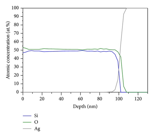
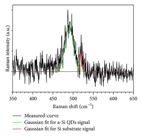
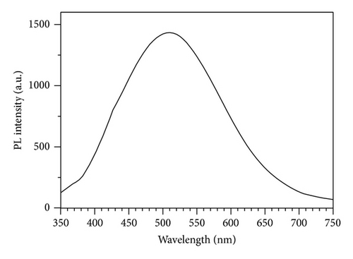
Figure 3(a) shows that the concentration-depth profiles of the SiOx:a-Si QDs film were performed by using Si 2p, O 1s, and Ag 3d peaks from XPS analysis. The average Si concentration of the SiOx:a-Si QDs film is about 48.27 at. %. High Si/O composition ratio for the SiOx:a-Si QDs film is observed, due to the high SiH4/N2O flow rate ratio of 5.53 : 1 during the PECVD growth. Since there are excessive Si atoms and insufficient O atoms, the Si atoms could move simply and accumulate to form a-Si QDs, without being restrained by Si-O bonds of the SiOx film during the annealing process [23, 24]. Hence, we conclude that the a-Si QDs can be synthesized at a low annealing temperature (300°C). The Ag atoms did not diffuse into the SiOx:a-Si QDs film from bottom Ag film after annealing process, as shown in Figure 3(a). Raman spectroscopy was used to analyze the size of Si QDs through the energy shift of the Raman peak and the correspondent line broadening [25]. Figure 3(b) shows that the Raman spectrum of SiOx:a-Si QDs film can be separated into two components. One component corresponds to the a-Si QDs, exhibiting a peak at 490 cm−1 with a FWHM of 33 cm−1. The Raman downshift and FWHM value show that the sizes of a-Si QDs are about 1.7 nm. Figure 3(c) presents the room-temperature PL spectrum of a-Si QDs LEDs without Ag grating structure (sample A), showing that the center emission wavelength is about 510 nm. The center emission wavelength of our 1.7 nm-sized a-Si QDs shows a good agreement with the theoretical study of light emission properties of SiOx:a-Si QDs film [20]. Hence, the existence of a-Si QDs embedded in the SiOx matrix with the low annealing process (300°C) is hereby proved by the Raman spectrum. Also, the main PL peak of a-Si QDs does not overlap with the PL spectrum from the oxygen related defects [26–28]. On the other hand, the smaller the a-Si QDs (~1.7 nm) are, the stronger the QCE is to surpass the interface state recombination [22, 29]. Hence, we conclude that the measured PL spectrum originates from the QCE of the a-Si QDs.
3.2. Optical Property Analysis (Sample A–D)
4. Conclusions
In conclusion, we proposed the plasmon-enhanced PL intensity of a-Si QDs LEDs with Ag/SiOx:a-Si QDs/Ag sandwich nanostructures resulting from the strong coupling between a-Si QDs and LSPPs modes. It was found that the LSPPs were excited underneath the Ag lines, which exhibit the Fabry-Pérot resonance resulting from the coupling of SPPs between the top Ag grating and bottom Ag film. A narrowest 67 nm FWHM of PL spectrum, a maximum of 4.8-fold PL enhancement factor, and the largest 2.46-fold PL integrated intensity, compared to the a-Si QDs LEDs without Ag grating structure, have been observed for an optimized Ag grating structure by the strong a-Si QDs-LSPPs coupling.
Conflict of Interests
The authors declare that there is no conflict of interests regarding the publication of this paper.
Acknowledgments
The authors would like to acknowledge the Ministry of Science and Technology of Taiwan for the financial support of this research under Contracts nos. MOST 102-2221-E-002-205-MY3 and MOST 104-3113-E-155-001 and National Taiwan University under the Aim for Top University Projects 104R7607-4 and 104R8908.


