Au/Cu2Te/CdTe/CdS/TCO/Glass Solar Cells with CdIn2O4 Obtained by Sol-Gel as TCO
Abstract
An Au/Cu2Te/CdTe/CdS/TCO/glass heterostructure based superstrate solar cells with 2.5 mm2 of area, where the CdTe layer was prepared by means of closed spaced sublimation (CSS) and the CdS by chemical bath, reached an efficiency (η) value of 12.1%. As transparent conductive oxide (TCO), a thin film of cadmium-indium oxide (CdIn2O4:CIO), obtained by sol-gel technique, was used. A systematic optimization of the thermal activation of the CdTe/CdS/CIO central part of the device with a CdCl2 vapor ambient made the conversion efficiency of the Au/Cu2Te/CdTe/CdS/CIO/glass heterostructure reaches 9.94% for the CdTe layer with thickness of 1.8 μm. This efficiency was reached only through an open circuit voltage (VOC) optimization. A maximum η of 12.1% was reached with the established procedure of optimization and when the CdTe layer thickness was increased to 3.1 ± 0.05 μm. The substitution of CIO by commercial ITO provoked in the cell a decrease of η from 12.1% to 7.2%, both devices prepared under the same conditions. Starting from these results, we can say that CIO was a better TCO than commercial ITO in our solar cell, with the advantage that CIO was obtained by sol-gel, which is a simple and economical technique.
1. Introduction
Cadmium telluride, one of the most promising materials for low cost terrestrial photovoltaic solar cells fabrication, has yielded a (a) 18.7% efficiency (η) record in small areas and (b) 14.4% in modules, according to First Solar, 2013 and 2012, respectively [1, 2]. This value is still lower than 29%, the theoretical maximum efficiency [3] which maintains the active experimental research on CdTe solar cells despite the slow progress observed in the last years. The lowest-cost solar cells are those fabricated as an all-thin-films device. The number of active layers establishes a commitment between low cost and maximum efficiency, nevertheless, a minimum number is needed to get a useful superstrate efficient solar cell: a transparent conductive oxide (TCO), an active semiconducting window, a semiconducting absorber, and a back contact. CdS has been constantly associated with high efficiency CdTe based solar cells as a window layer; however, for TCO, a wide variety exists, most times SnO2 based layers are employed, that is, doped or undoped SnO2, indium tin oxide (ITO), cadmium tin oxide, zinc tin oxide, and Cu-ITO. In the same way, the back contact to CdTe has also been varied, and despite the preparation of ohmic contacts to CdTe, it is not an easy task; several conductive layers have been used with excellent results: Au-Cu, Cu2Te, Mo, and so forth. At least a dozen of different transparent conductive oxides have been employed in CdTe based all-inorganic solar cells, whether with or without a CdS window layer, during the last forty years. However, not all of them have worked as good TCO for acceptably efficient solar cells (≥10%). Among them, diamond [4], TiO2 [5], and TiO2-SiO2 [6] are the less common TCO’s used, which have yielded to date, in general, poor results. Nevertheless, transparent carbon nanotubes have provided good results in CdS/CdTe based solar cells [7]. Very recently, data on CdS/CdTe solar cells performance with efficiencies in the range 12.6–16.5% and reported during a 20-year interval (1991–2010) has been published [8]. In support of the aforementioned fact, almost all the photovoltaic devices of that work are constituted of TCOs based on tin oxide, whereas the cadmium indate, CdIn2O4 (CIO), is not present. As a matter of fact, CIO has practically never been used in the preparation of solar cells even after it has been widely studied and also recommended in the last years as a good TCO for photovoltaic devices fabrication [9]. CIO has been characterized as a material with very high transparency and high conductivity [9, 10], which are the most important properties for a good TCO in solar cells. In this work, the preparation of CdTe/CdS solar cells with the basic heterostructure Au/Cu2Te/CdTe/CdS/TCO/glass by utilizing CIO as TCO is reported. The efficiency of the cell is significantly increased when the home-made CIO is used as TCO instead of commercial ITO, by keeping the rest of preparation conditions constant. With the optimization of the CdTe layer with respect to oxygen partial pressure used during the growth, the increase of CdTe layer thickness, and also with the optimization of the annealing parameters for the activation process in CdCl2 vapor (on the CdTe/CdS/TCO/glass), the determination of the optimal values to obtain the highest open circuit voltage to reach η = 12.1% in circular areas (A = 0.025 cm2, diameter = 0.18 cm) was obtained. When ITO was used as TCO, under the same growing and design conditions, η was reduced to 7.2%. This result shows the high quality of our CIO as TCO.
2. Experimental
The preparation and the physical properties of the cadmium indate obtained by sol-gel, for the cells studied here, have been previously reported by us [11]. Both the optical window (absorption edge) and the transparency of the CIO layers were increased after the thermal treatment in vacuum for one hour. In Figure 1, the optical transmittance in the UV-Vis region of CIO films, without annealing, only sintered in air at 550°C for 1 h (not annealed) and with annealing (annealed) when the CIO film is subjected at a second thermal treatment in vacuum, is displayed. In the same figure, the spectrum of the commercial ITO used in this work is shown. The CdTe films were deposited using a close-spaced sublimation (CSS) system manufactured in our lab. The films were deposited on CdS/CIO/glass substrates in an Ar-O2 ambient at 150 mbar. Four different partial pressures of O2 () were employed, namely, 1, 3, 5, and 10%. First, the chamber was evacuated to a pressure of 1 × 10⁻⁵ mbar and when the gases were introduced to the system, the pressure was raised to 150 mbar. CdTe powder of 99.99% purity (256544 Aldrich) put at the bottom of the graphite container of the lower heater (source) was used as target. The space between the source and the substrate was 3 mm. For all the films, the source temperature (TSou) was 625°C and the substrate temperature (TSub) 525°C, which is the same as that of the upper graphite heather. The CdTe layer growing time was 15 min for a CdTe thickness of 1.8 ± 0.05 μm and for the thickness 3.10 ± 0.05 μm 30 min was used. General properties of our CSS-CdTe films were already published [12]. The CdS layers were deposited by chemical bath (CB) following a procedure already reported [13], but the solution was prepared at different molar concentrations. The exact amounts of the reagents and the molarities are given in Table 1.
| Reagent | Concentration | Exact amount used for aqueous bath |
|---|---|---|
| Cadmium acetate | 0.0391 M | 172.5 mg |
| Ammonium acetate | 0.785 M | 1.0026 g |
| Thiourea | 0.1752 M | 220.2 mg |
| Ammonium hydroxide | 28–30% | 36.9 mL |
| H2O | — | 450 mL |

Resistivity of CdTe films (deposited at a of 3%) was measured by the two-probe method with a Hewlett Packard 4329A high resistance meter, because it is too high, under illumination 1.9 × 10⁶ Ω-cm (using our simulator solar) and in darkness 3.8 × 10⁸ Ω-cm. However, resistance per square of CIO, CIO/CdS, ITO, and ITO/CdS films (Table 2) was obtained by a linear four-point probe using a Loresta-GP low resistivity meter (MCP-T600).
| Layers/glass | R□ (Ω/□) without additional TT | R□ (Ω/□) with additional TT |
|---|---|---|
| CIO | 40–60 | 21–18 |
| CdS/CIO | 21–18 | 21–18 |
| ITO | 7.5 | 40 |
| CdS/ITO | 7.5 | 40 |
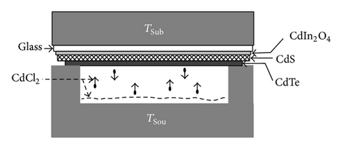
For the open circuit voltage optimization of the CdTe/CdS/CdIn2O4/glass heterostructures, a thermal annealing in CdCl2 vapor was applied by employing a similar CSS system used to deposit the CdTe layer (see Figure 2). Three CdCl2-vapor annealing processes at a pressure of 1 × 10⁻⁵ mbar were made as follows. (i) For each O2 partial pressure used in the CdTe layers growth, keeping TSou = 380°C and TSub = 420°C constant, the annealing time (tAnn) was varied in the interval 5–30 min in steps of 5 min. (ii) With TSou = 380°C constant, TSub was varied in the range 380–435°C in steps of 5°C with CdTe grown at = 3% and tAnn kept fixed at 20 min. (iii) TSub was constant at 420°C, and TSou was varied in the interval 350–410°C, with = 3% and tAnn = 20 min. For the VOC measurements, graphite contacts were employed with the purpose to avoid short circuits between TCO and back contact, due to the possible presence of pinholes, since graphite paste eliminates this problem. In addition, graphite is an ohmic contact on CdTe with no thermal treatment; however, low current densities are expected due to the lack of intimate contact between CdTe and graphite paste, because of the superficial roughness of CdTe [12].
For the current-voltage measurements, Au/Cu2Te back contacts were evaporated following a procedure reported [14]. In our case, 0.00362 mg of Cu2Te was deposited at a source-sample distance of 40 mm. After that, 0.0035 mg of Au was also deposited at the same distance. Cu2Te and Au thin thickness was 57.4 nm and 64.4 nm, respectively. Finally, an annealing in vacuum during 1 min was done. Twenty-five Au/Cu2Te circular contacts (cells) of area = 0.025 cm2 were distributed equidistantly on samples of 2.0 × 2.0 cm2. The area of these contacts was carefully measured by means of an optical microscope.
Cross-section of the heterostructure was observed using a scanning electron microscope (SEM) Philips XL30-ESEM. Thickness of the CdS film was measured using a Sloan Dektak II profilometer. Open circuit voltage (VOC) and short circuit density current (JSC) were measured using a solar simulator made in our lab, which is constituted of a set of Q50MR16/CG/47/10 Solux Lamps. This lamp has a solar spectrum very similar to the sun in particular in the 350 nm to 800 nm spectral region [15]. The power irradiated measured over the solar cell was of 90 mW/cm2. Serie and shut resistances were calculated starting from the analysis reported by Bouzidi et al. [16]. All the characterization was carried out at room temperature.
3. Results and Discussion
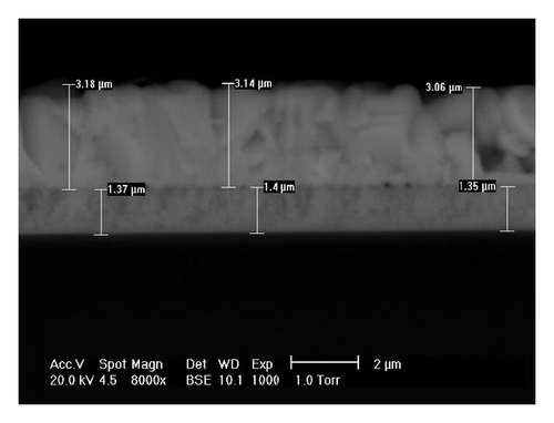
An image of a cross-section of the CdTe/CdS/CIO heterostructure is exhibited in Figure 3. According to the image, the thickness of the CdTe layer is 3.10 ± 0.05 μm and that of CIO is 1.40 ± 0.05 μm. It is not possible to see the CdS layer because its thickness is approximately 200 nm, which was measured by a profilometer. This thickness was the same independent if whether the CdS layer was deposited on CIO or ITO.
X-ray diffraction patterns (not shown) indicate that the crystalline structure of the CdTe films is cubic-zincblende and that of the CdS films is hexagonal-wurtzite, and, in both cases, the layers are constituted of polycrystalline material. In order to obtain Au/Cu2Te/CdTe/CdS/TCO/glass solar cells with high efficiency, the main step was the optimization of the activation process of the CdTe/CdS/CIO/glass heterostructure by a systematic variation of the CdCl2-vapor thermal annealing parameters to reach the highest VOC value. Later, the CdTe layer thickness was increased.
Initial data measurements (, tAnn, TSou, and TSub) for the best value of VOC were submitted to feedback in such a manner that values shown in Figures 4, 5, and 6 are the resultant measurement of that feedback process.
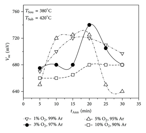
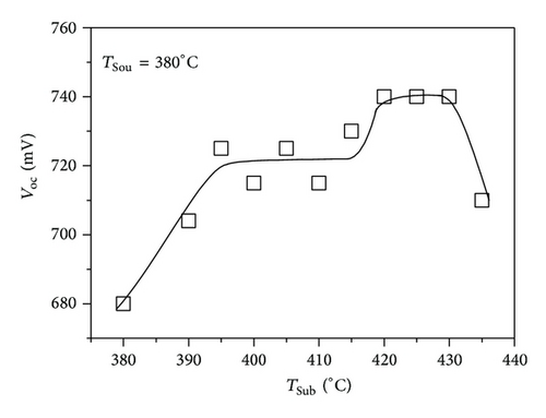
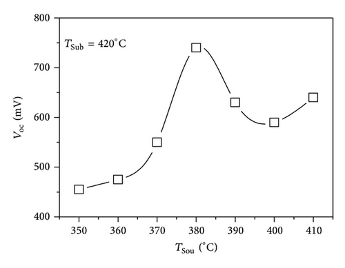
Firstly the CdTe layer thickness was fixed at 1.8 μm. In the annealing in CdCl2 vapor, TSub always was higher or equal to TSou (TSub≥TSou) with the purpose of preventing the formation of a CdCl2 layer on the CdTe surface. In Figure 4, data of VOC versus tAnn in the 5–30 min range are plotted for the different values used, maintaining constant TSou and TSub at 380 and 420°C, respectively. This is step (i) described in the experimental section. The maximum VOC observed is that which corresponds to tAnn = 20 min and = 3%. (ii) With these two values (tAnn and ) and with TSou = 380°C, the three parameters are constant, and VOC is plotted against TSub in the 380–435°C interval. Here, VOC is the maximum in the 420 ≤ TSub ≤ 430°C region, which is displayed in Figure 5. (iii) For tAnn = 20 min, = 3%, and TSub = 420°C constants, VOC as a function of TSou in the range 350–410°C, VOC maximum occurs for TSou = 380°C, as can be observed in Figure 6.
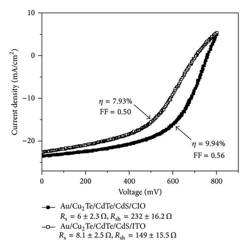
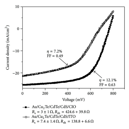
Au/Cu2Te/CdTe/CdS/CIO/glass heterostructure-solar cells were manufactured under the preparation conditions to obtain the highest value of VOC by means of the thermal annealing in CdCl2 vapor (indicated in Figures 4, 5, and 6) and a CdTe thickness of 1.8 μm. The average values and their respective standard deviations for VOC, JSC, and fill factor (FF) were 753 ± 27 mV, 23.56 ± 0.53 mA/cm2, and 0.56 ± 0.02, respectively, giving an average efficiency value of 9.94%. Notice that the VOC value is practically the same as the one obtained in the optimization process of VOC using graphite contacts (Figures 6 and 7(b)). When the CdTe layer thickness was increased to 3.10 ± 0.05 μm, the photovoltaic parameters obtained were JSC = 25.17 ± 0.5 mA/cm2, VOC = 767 ± 16 mV, and FF = 0.63 ± 0.01. With these data, the photovoltaic conversion efficiency reaches an average value of 12.1%. The average values of the photovoltaic parameters were calculated on twenty-five solar cells, each with 0.025 cm2 of area. Typical photovoltaic responses of the Au/Cu2Te/CdTe/CdS/CIO/glass solar cells with CdTe layer thickness of 1.8 μm and 3.1 μm are shown in Figures 7(a) and 7(b), respectively. The same figures also show the photovoltaic response of the Au/Cu2Te/CdTe/CdS/ITO/glass solar cells, using the same deposition parameters and the optimization process of the CdCl2 vapor activation. Commercial ITO film was used with nominal coating thickness in the 150 to 200 nm range. It is important to point out that, after sintering under an open atmosphere, the sheet resistance of the CIO layer used in the cell was between 40 and 60 Ω/□ (resistivity ~8 × 10⁻³ Ω-cm). The resistance of the CIO decreased even more until 18 Ω/□, after the deposition of the CdS layer, as measured using contacts placed on the CdS layer. By considering the high resistivity of CdS [17], this last value of sheet resistance measured actually corresponds to that of the CIO layer. When the CIO layer and CdS/CIO layers are submitted to an additional thermal treatment, with similar conditions to those of deposition of CdTe, the sheet resistance of CIO (without CdS layer) decreases and CdS/CIO does not change (Table 2). From these results, we can ensure that the deposit of CdS layer contributes to decrease the resistivity of the CIO and also that the additional treatment provokes a decrease of the CIO resistivity. However, this fact was not observed for commercial ITO and an increase of the sheet resistance was observed with the additional thermal treatment (Table 2). On the other hand, series (Rs) and shut (Rsh) resistances obtained for both solar cells types are shown in Figure 7. A lower Rs and higher Rsh value for the solar cell can be seen where CIO is used as TCO, which corroborate the quality of the CIO obtained by sol-gel.
Different authors have reported several disadvantages of ITO layers as compared with other TCOs. It has been found that SnO2:F is chemically and thermally more stable than ITO in solar cells fabrication [18, 19]. Also, the CdS/ITO heterojunction shows a rectifier effect which was not found in the CdS/SnO2 bilayers; this fact is reflected in the performance of a solar cell [20]. High efficiencies have been reported using SnO2:F/SnO2 bilayer in CdS/CdTe photovoltaic solar cells [21]. Several years ago, Granqvist had reported that ZnO:Al is a more promising TCO than ITO to fabricate thin films solar cells [22]; in 2003, a 14% efficiency was reported in ZnO:Al/CdS/CdTe solar cell structure [23]. In our case, we have found how CIO prepared by sol-gel is more stable and capable of improving its conductivity under thermal treatments than commercial ITO when it is used as TCO for CdTe/CdS/TCO solar photovoltaic devices. Work is in progress to study in more detail the properties of the CIO/CdS/CdTe heterostructure.
4. Conclusions
From this work, we can say that CIO is a better TCO than commercial ITO in our solar cell, with the advantage that CIO is obtained by sol-gel, which is a simple and economical technique. A solar cell of Au/Cu2Te/CdTe/CdS/TCO/glass heterostructure was obtained with efficiency of 12.1% when our CIO was used as TCO and a diminishing to 7.2% was obtained when CIO is substituted by ITO commercial.
Conflict of Interests
The authors declare that there is no conflict of interests regarding the publication of this paper.
Acknowledgments
This work was supported by Consejo Nacional de Ciencia y Tecnología (CONACyT) under Project CB-2008-01-106392 and Instituto de Ciencia y Tecnología del Distrito Federal under Project ICyTDF/341/2010 and ICyTDF/258/2012. The authors wish to thank, M.S., Cynthia I. Zúñiga Romero and, M.S., Adair Jiménez Nieto for their technical assistance.


