Ultra-Low-Voltage Low-Power Bulk-Driven Quasi-Floating-Gate Operational Transconductance Amplifier
Abstract
A new ultra-low-voltage (LV) low-power (LP) bulk-driven quasi-floating-gate (BD-QFG) operational transconductance amplifier (OTA) is presented in this paper. The proposed circuit is designed using 0.18 μm CMOS technology. A supply voltage of ±0.3 V and a quiescent bias current of 5 μA are used. The PSpice simulation result shows that the power consumption of the proposed BD-QFG OTA is 13.4 μW. Thus, the circuit is suitable for low-power applications. In order to confirm that the proposed BD-QFG OTA can be used in analog signal processing, a BD-QFG OTA-based diodeless precision rectifier is designed as an example application. This rectifier employs only two BD-QFG OTAs and consumes only 26.8 μW.
1. Introduction
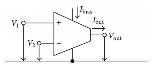
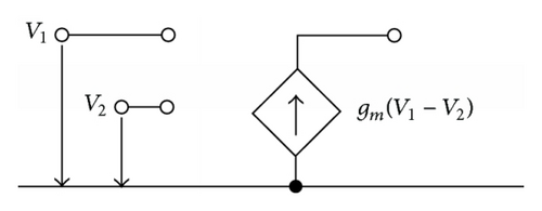
In the late sixties, the Radio Corporation of America (RCA) and then General Electric (GE) came out with the operational transconductance amplifier, hereafter called OTA. The name means essentially a controllable resistance amplifier. OTA is a key functional block used in many analog and mixed-mode circuits. It is a special case of an ideal active element, and its implementation in IC form makes it indispensable today in discrete and fully integrated analog network design. The ideal OTA as shown in Figure 1 can be considered as a differential voltage-controlled current source (DVCCS); its transconductance “gm” represents the ratio of the output current to the differential input voltage, that is, Iout/(V1 − V2). This transconductance is used as a design parameter and it is usually adjustable by the amplifier bias current (Ibias). The benefit of this adjusting possibility is acquiring the ability of electronic orthogonal tunability to circuit parameters. It could be noted that tunability has a main role in integrated circuits, especially to satisfy a variety of design specifications. Thus, OTA has been implemented widely in CMOS and bipolar and also in BiCMOS and GaAs technologies [1].
The OTA is similar to the standard operation amplifier (OPA) in the sense of infinite input impedances, but its output impedance is much higher and that makes OTA more desirable than any ordinary amplifier. Recently, the multiple-output-OTA (MO-OTA) has been introduced and used, on par with the ordinary operation amplifier, as a basic block in many applications, particularly for realizing universal filters which are able to implement several second-order transfer functions with a minimum of adjustments. The literature provides numerous examples of OTA-based biquad structures, as well as active elements such as current conveyor (CC), current differencing transconductance amplifier (CDTA), current-through transconductance amplifier (CTTA), and current-conveyor transconductance amplifier (CCTA).
The symbol and the equivalent circuit of ideal OTA are shown in Figures 1(a) and 1(b), respectively [1]. Simple applications of the OTA include voltage amplification, voltage-variable resistor (VVR), voltage summation, integration, gyrator realization, practical OTAs, current conveyor, and active RC filters. In addition, one of OTA’s principal uses is in implementing electronically controlled applications such as variable frequency oscillators and variable gain amplifier stages which are more difficult to implement with standard OPAs.
Recently, Low power analog circuit design is undergoing a very considerable boom. However, circuit designers encounter difficulties to preserve reliable performance of the analog circuits with scaling down their supply voltage, owing to the fact that the threshold voltage and supply voltage are not decreased proportionally. Hence, various techniques based on CMOS technology have emerged to overcome the rather high threshold voltage problem of MOS transistors, such as unconventional MOS techniques, that is, floating-gate (FG), quasi-floating-gate (QFG), bulk-driven (BD), bulk-driven floating-gate (BD-FG), and bulk-driven quasi-floating-gate (BD-QFG) MOS transistor [2, 3]. Utilizing these techniques offers circuit simplicity, high functionality, extended input voltage range, and ultra-LV LP operation capability. Thus, they are very suitable for ultra-LV LP applications as battery-powered implantable and wearable medical devices.
In this paper, The BD-QFG technique has been chosen to be utilized to build LP LV OTA, since it enjoys higher transconductance value, higher bandwidth, and smaller input referred noise in comparison with other unconventional techniques. To verify the functionality of the proposed OTA voltage mode diodeless precision rectifier is introduced in this work.
The organization of this paper is as follows: in Section 2 the CMOS internal structure of the BD-QFG OTA is described. In Section 3 the principle of BD-QFG OTA-based diodeless precision rectifier is presented. The simulation results are provided in Section 4; eventually, Section 5 is the conclusions.
2. Bulk-Driven Quasi-Floating-Gate Operational Transconductance Amplifier (BD-QFG OTA)
The circuit, which is shown in Figure 2, consisted of two stages. The first stage consists of BD-QFG differential input M1 and M2. The gates of these transistors are tied to the negative supply voltage VSS through extremely high value resistors constructed by transistors Mb1 and Mb2 which are operating in cutoff region. The input terminals are connected to M1 and M2 from two sides: capacitively coupled to the quasi-floating-gates via C1 and C2 from one side and connected to bulk terminals from the other side.
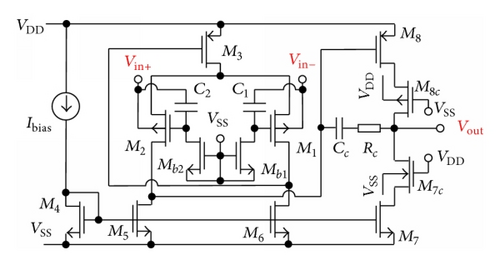
Transistors M4, M5, M6, and M7 act as a multiple output current mirror applying the constant current source Ibias to each branch of the circuit. Transistors M5 and M6 form the active load and transistor M3 acts as tail current source for the differential input stage. The input voltage terminals are connected to the bulk terminals of M1 and M2; therefore, high input impedance is achieved.
Equation (1) shows the capability of the proposed BD-QFG OTA structure for operation under lower supply voltage.
3. BD-QFG OTA-Based Diodeless Precision Rectifier
A precision rectifier is one of important nonlinear circuits, which is extensively used in analog signal processing systems. In precision rectification, a bidirectional signal is converted to one-directional signal. Typically, a conventional rectifier could be realized by using diodes for its rectification, but diode cannot rectify signals whose amplitudes are less than the threshold voltage (approximately 0.7 V for silicon diode and approximately 0.3 V for germanium diode). As a result, diode-only rectifiers are used in only those applications in which the precision in the range of threshold voltage is insignificant, such as RF demodulators and DC voltage supply rectifiers, but for applications requiring accuracy in the range of threshold voltage the diode-only rectifier cannot be used. This can be overcome by using integrated circuit rectifiers instead.
Traditional methods of realizing precision rectifier circuits include the use of operational amplifiers, resistors, and either diodes [5–9] or alternating source-followers [10]. A number of current conveyors-based current-mode rectifier circuits were introduced in the literature [7, 11–16]. The rectifier circuits in [11–13] employ diodes and resistors in addition to second generation current conveyors (CCIIs). The circuit proposed in [7] employs bipolar current mirrors in addition to a CCII and a number of resistors. The rectifier circuit in [14] employs four current controlled conveyors (CCCIIs) and resistors. However, the use of resistor makes these circuits not ideal for integration. Therefore, precision rectifiers by using all-MOS transistors are proposed [17–26]. Authors in [27] proposed a circuit which employs two CCIIs and two MOS transistors. Authors in [28] presented a circuit which employs an amplifier and a simple voltage comparator. Author in [27] introduced a rectifier which employs two differential difference current conveyors (DDCCs). A new technique for realizing a precision half-wave voltage rectifier in CMOS technology is proposed; this technique is based on bulk-driven quasi-floating-gate operational transconductance amplifier (BD-QFG OTA).

It is worth mentioning that the same configuration shown in Figure 3 could be used as full-wave rectifier just by applying Vin (an identical signal of Vin shifted 180°) to Voff terminal.
4. Simulation Results
The proposed BD-QFG OTA was designed and simulated using TSMC 0.18 μm N-well CMOS. The used PSpice model is available on [29]. The supply voltage was ±0.3 V, the biasing current was Ibias = 5 μA. and the power consumption was 13.4 μW. The optimal transistor aspect ratios and the values of components are given in Table 1. Table 2 shows a list of measured operational amplifier benchmarks used to evaluate proposed OTA. Features of the circuit (shown in Figure 2) are listed in the first column, along with values of other works listed in other columns.
| BD-QFG OTA | W/L [μm/μm] |
|---|---|
| M1, M2 | 20/0.3 |
| Mb1, Mb2 | 30/2 |
| M3, M8 | 100/0.3 |
| M4, M5, M6 | 4/0.3 |
| M7 | 8/0.3 |
| M7c | 45/2 |
| M8c | 100/2 |
| C1 = C2 = 0.4 pF | |
| Rc = 10 kΩ, Cc = 3 pF | |
| Parameters | This work | Koziel and Szczepanski [33] | Majumdar [34] | Li and Raut [35] | Zhang et al. [36] |
|---|---|---|---|---|---|
| CMOS technology | |||||
| [μm] | 0.18 | 0.5 | 0.35 | 0.35 | 0.18 |
| Power supply | |||||
| [V] | ±0.3 | ±2.5 | 3.3 | 3.3 | 1.8 |
| Power consumption | |||||
| [μW] | 13.4 | 6800 | 3370 | 2330 | 590 |
| Transistors number | |||||
| [/] | 12 | 37 | 14 | 22 | 68 |
| AC gain | |||||
| [dB] | 51 | 65 | 80.4 | 65 | 55 |
| Linearity range | |||||
| [mV] | ±0.3 | ±0.75 | ±0.1 | / | ±0.27 |
| Output resistance | |||||
| [MΩ] | 0.317 | 3.4 | / | 1.2 | 8.3 |
| −3 dB bandwidth | |||||
| [MHz] | 59 | 100 | 123.2 | 100 | 200 |
Figure 4 shows the simulated magnitude of output impedance of OTA. Zout is high as expected; its value is 7.83 MΩ. The AC gain and phase responses of the BD-QFG OTA with 3 pF load capacitance are shown in Figure 5. The open-loop gain is 80 dB and the gain-bandwidth product is 6.4 MHz. The phase margin is 65° which guarantees the circuit stability. The voltage follower frequency response of the proposed circuit is shown in Figure 6. The cutoff frequency is about 15 MHz.
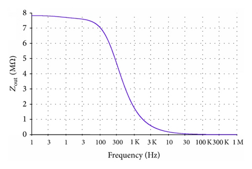

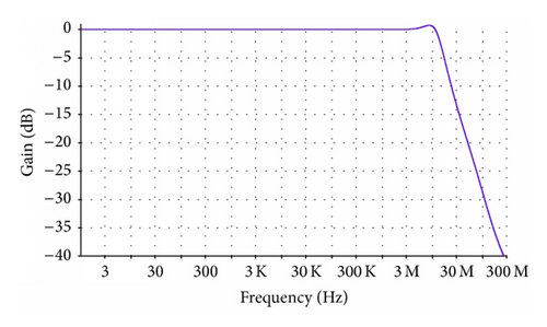
Figure 7 presents the DC transfer characteristic of the BD-QFG OTA. For input voltage range from −266 to 266 mV the voltage error is below 4 mV. Therefore, using Voff = 0 V and maximum input amplitude Vm·max of ±250 mV, the OTA is not expected to have strong impact on the overall rectifier accuracy.

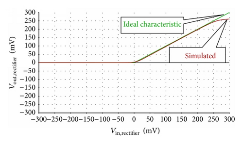
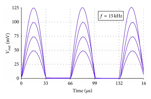
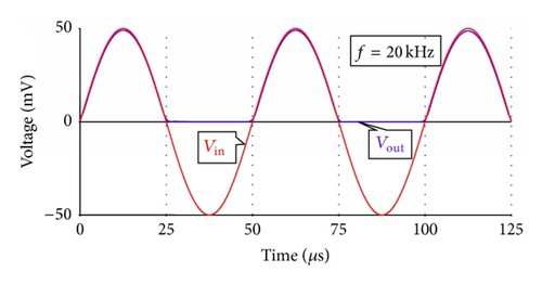
The diodeless half-wave precision rectifier shown in Figure 3 was simulated using BD-QFG OTA shown in Figure 2. The supply voltage of ±0.3 V and the bias current of Ibias = 5 μA for OTAs were used. The circuit consumes 26.8 μW. Figure 8 shows the DC transfer characteristic of BD-QFG half-wave rectifier in comparison with the ideal one and it confirms the precise rectification for input amplitude ranging ±250 mV. Figure 9 shows the transient response of the output waveforms for input signal of 15 kHz and amplitudes from 50 mV to 125 mV with step of 25 mV. Hence, the rectifier is capable of rectifying a wide range of amplitudes. Figure 10 shows the transient responses of the input and output waveforms with amplitude of 100 mV and frequency of 20 kHz, 30 kHz, 40 kHz, and 50 kHz. The load capacitor Cload for simulations done in Figures 9 and 10 was set to 5 pF.
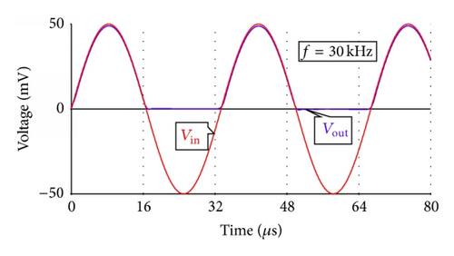
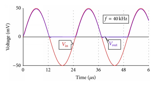
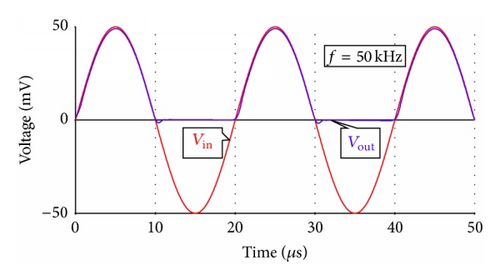
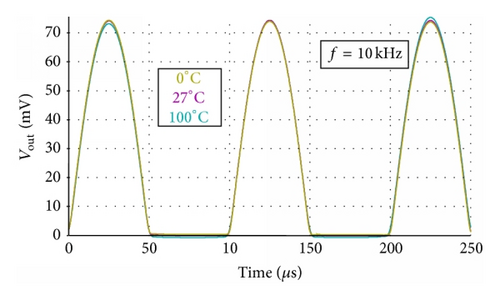
To demonstrate the temperature performance of proposed circuit, the proposed circuit was simulated at the frequency of 10 kHz by changing temperature. Figure 11 shows the output waveforms of the proposed rectifier at temperatures of 0°C, 27°C, and 100°C. From Figure 11, it can be seen that the proposed circuit provides excellent temperature stability without any compensation technique.
Here, the suffix RMSE is an abbreviation of the term “root mean square error.” For ideal circuit operation, that is, vout(t) = videal(t), the result is PRMSE = 0, while in the case of total attenuation of the output signal PRMSE = 1. For extra high distortions, when the mutual energy of signals vout and videal can be negative, one can obtain PRMSE > 1. Figure 12 shows the PAVR (a) and PRMSE (b) versus frequency in range of 10 kHz up to 500 kHz for three amplitudes of the input voltage (50, 100, and 150) mV. As one can notice from the figure, over the full range of frequency, the value of PAVR ranges from 1 to 0.85 and the value of PRMSE is below 0.1. The values of PAVR and PRMSE achieved confirm the quality of the rectification process of the proposed rectifier.
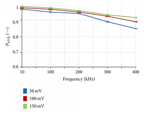
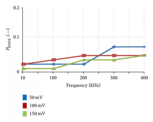
Table 3 provides comparison of the proposed rectifier with three half wave rectifiers introduced in [30–32]. To compare their performance figure of merit FOM is provided, which indicates the efficiency of the design regarding the maximum allowable input swing over voltage supply. Higher value of the FOM translates proportionate advantage in terms of input voltage range. It is notable that the proposed rectifier possesses the highest value of FOM. Besides, the proposed rectifier offers the highest maximum frequency with ultra-LV operation capability and simple CMOS internal structure.
| Parameter | Proposed rectifier | [30] | [31] | [32] |
|---|---|---|---|---|
| Technology used | ||||
| [μm] | 0.18 | 1.5 | 0.18 | 0.35 |
| Supply voltage | ||||
| [V] | ±0.3 | 2.8 | 1.8 | 1 |
| Power consumption | ||||
| [μW] | 13.4 | 2.8 | 1.08 | 0.06 |
| Maximum amplitude | ||||
| [mV] | 225* | 850 | 630 | 230 |
| Maximum frequency | ||||
| [kHz] | 400* | 10 | 20 | 0.1 |
| FOM** | ||||
| % | 37.5 | 30 | 35 | 23 |
- *0.85 ≤ PAVR ≤ 1, 0 < PRMSE < 0.1.
- **FOM = (maximum amplitude/supply voltage) * 100.
5. Conclusions
In this paper, a new ultra-low-voltage supply and low-power consumption BD-QFG OTA is presented. The active building block was simulated using TSMC 0.18 μm N-well CMOS technology. It is demonstrated that the proposed BD-QFG OTA can operate at ±0.3 V supply voltage and consumes 13.4 μW of static power. The proposed BD-QFG OTA is used to realize diodeless precision rectifier as an example application. Proposed BD-QFG OTA could be used in LV and LP applications such as bioelectronics, biosensors, and biomedical systems. The simulation results confirm the workability of the active building block.
Conflict of Interests
The authors declare that there is no conflict of interests regarding the publication of this paper.
Acknowledgments
The described research was performed in laboratories supported by the SIX project, registration no. CZ. 1.05/2.1.00/03.0072, the operational program Research and Development for Innovation, and has been supported by Czech Science Foundation Project no. P102-14-07724S.


