Surface State Capture Cross-Section at the Interface between Silicon and Hafnium Oxide
Abstract
The interfacial properties between silicon and hafnium oxide (HfO2) are explored by the gated-diode method and the subthreshold measurement. The density of interface-trapped charges, the current induced by surface defect centers, the surface recombination velocity, and the surface state capture cross-section are obtained in this work. Among the interfacial properties, the surface state capture cross-section is approximately constant even if the postdeposition annealing condition is changed. This effective capture cross-section of surface states is about 2.4 × 10⁻¹⁵ cm2, which may be an inherent nature in the HfO2/Si interface.
1. Introduction
Hafnium oxide (HfO2) has emerged recently as an essential dielectric material in the semiconductor industry, currently being used in logic gate stacks [1] and considered a promising candidate for resistance switching memory devices [2, 3] as well as surface passivation of advanced Si solar cells [4, 5]. Therefore, the determination of surface state capture cross-section at the interface between silicon and hafnium oxide is of great importance for the semiconductor industry, the photovoltaic industry, and the scientific community. The known characteristics of HfO2 thin films include a large band gap (~6 eV) [6], a relatively high dielectric constant (>20) [7], an acceptable breakdown strength (>4 MV/cm) [7], excellent thermodynamic stability [8], and an effective mass of carrier transportation [9]. In this work, the interface characteristics of the interface-trapped charge density (Nit), the interface-trapped charge density per area and energy (Dit), the effective capture cross-section (σs) of surface states, the surface recombination velocity (so), and the minority carrier lifetime (τFI J) are identified. The typically electrical measurements of current-voltage (I-V) and capacitance-voltage (C-V) characteristics were performed on the Al/HfO2/p-Si metal-oxide-semiconductor (MOS) capacitors and metal-oxide-semiconductor field-effect transistors (MOSFETs). Both gated-diode method [10, 11] and subthreshold measurement [12] were applied to evaluate the capture cross-section of interface states for the HfO2-gated MOSFETs. The gated-diode method is a simple way to accurately identify the interfacial characteristics using only a sweeping dc gate voltage, which was introduced in 1966 by Grove and Fitzgerald [10] to determine the surface-state density in MOS structures. According to the gated-diode measurements, the surface recombination velocity and the minority carrier lifetime (τFI J) in the field-induced depletion region were extracted. In addition, the interface-trapped charge density per area and energy (Dit) was determined by using the device subthreshold measurement. Consequently, the effective capture cross-section of surface states was determined to be about 2.4 × 10⁻¹⁵ cm2 by the combination of gated-diode and device subthreshold measurements.
2. Experiment
Here, (100) p-type silicon wafers (1–5 Ω-cm) were used as the starting material. Following the standard cleaning procedures, a 500 nm SiO2 film was grown on silicon wafers by wet oxidation. The source and drain windows were defined by wet etching and doped by phosphorous diffusion. The HfO2 films were deposited by RF magnetron sputtering in argon ambient at room temperature. The flow rate of argon was 13.5 standard cubic centimeters per minute (sccm). The total pressure during deposition was 20 mtorr. The refractive index, energy bandgap, and thickness of these thin films were measured by an N&K analyzer. The optical refractive index (n) and energy bandgap (EG) were around 1.9–2.1 and 5.6–5.8 eV, respectively. The deposited thicknesses of HfO2 thin films ranged from 12 nm to 47.1 nm. After HfO2 deposition, the postdeposition anneal (PDA) was performed in either N2 or N2/O2 (i.e., 50% N2 and 50% O2) with a flow rate of 3 sccm for 60 s at 500°C. According to the X-ray diffraction analysis, the HfO2 films annealed at 500°C were amorphous. The aluminum (Al) electrodes were evaporated and patterned using a wet etching process. Postmetallization annealing (PMA) was performed at 400°C in N2 for 30 s. The Al/HfO2/p-Si MOS capacitors and MOSFETs were measured by Agilent 4156C semiconductor parameter analyzer and Agilent 4284A impedance analyzer. All the measurements were performed under dark condition. Based on the high-frequency (1 MHz) C-V measurements for the MOS capacitors, the effective dielectric constant of HfO2 films annealed at 500°C in N2 or N2/O2 was evaluated as 18.9 or 19.3, respectively (not shown here). In this work, the relatively large devices were chosen to avoid the short channel effects which may cause the distortion in analysis of surface state capture cross-section. The channel width (W) is 100 μm and the channel length (L) is 19 μm.
3. Results and Discussion
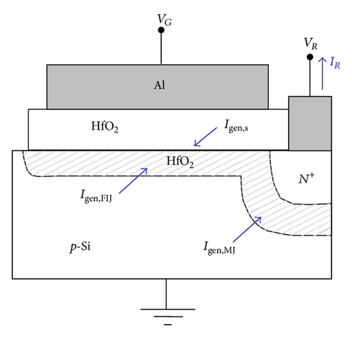
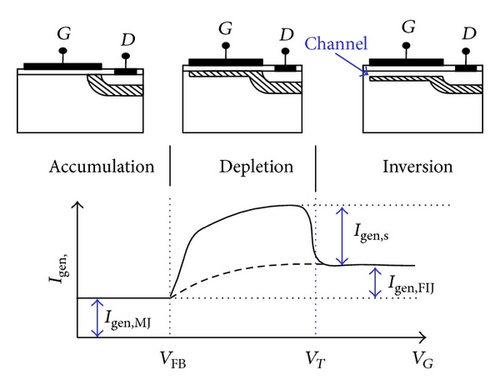
Figure 2 shows the reverse diode current IR versus VG for the HfO2 gated-diodes at VR = 2 V. Through the gated diode method, the surface recombination velocity (so) and the minority carrier lifetime (τFI J) in the field-induced depletion region can be extracted. For HfO2 films annealed in N2/O2, so and τFI J are determined to be 4.1 × 103 cm/s and 16 ns. On the other hand, for HfO2 films annealed in N2, so and τFI J are determined to be 8.9 × 103 cm/s and 22 ns. Obviously, the reverse diode current of nMOSFETs for HfO2 annealed at 500°C in N2/O2 is smaller than that annealed in N2. The reduction in reverse current may be attributed to the decrease in oxygen vacancy related defects [16–19] in HfO2. The oxygen vacancy is one type of trapping centers and is easily formed in HfO2 due to the transportation of oxygen atoms from HfO2 into Si [18, 19]. During the thermal treatment of PDA in N2/O2 ambient, the oxygen atoms can diffuse into the HfO2 films to partially passivate the existing oxygen vacancies. Hence, the reverse diode current can be reduced by N2/O2 annealing.
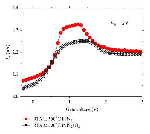
Figure 3 shows the IDS-VGS characteristics. The Ion /Ioff ratio is larger than 106 at VD = 0.05 V, indicating that the nMOSFETs with amorphous HfO2 gate dielectrics have a good current switch capability. The subthreshold swings (St) for the HfO2 gate dielectrics annealed at 500°C in N2 and N2/O2 are about 85.1 and 76.4 mV/dec, respectively. According to Figure 3, the density of interface traps per area and energy (Dit) can be determined from the subthreshold swing measurement, because St is expressed as 2.3(kT/q)[1 + (CD + Cit)/Cox] [12], where CD is the depletion-layer capacitance, Cit is the capacitance associated with the interface traps, and Cox is the dielectric capacitance. The determined Dit is about 4.6 × 10¹² and 2.1 × 1012 cm−2-eV−1 for HfO2 annealed at 500°C in N2 and N2/O2, respectively. Once Dit is determined, σs and Nit can be extracted using (4). For HfO2 annealed in N2, σs and Nit are extracted to be about 2.4 × 10⁻¹⁵ cm2 and 3.7 × 1011 cm−2, respectively; for HfO2 annealed in N2/O2, σs and Nit are extracted to be 2.4 × 10⁻¹⁵ cm2 and 1.7 × 1011 cm−2, respectively. It is worthy of note that the same σs value is obtained for HfO2 annealed both in N2 and in N2/O2. This finding may imply that the capture cross-section of surface states is an inherent nature at the HfO2/Si interface. The universal constant of surface state capture cross-section is around 2.4 × 10⁻¹⁵ cm2.
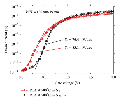
Figure 4 shows the channel electron mobility versus the effective electric field. The effective surface field (Eeff) and effective channel mobility (μeff) can be expressed as Eeff = (0.5Qinv + QB)/εSi and μ = (IDS/VDS)(L/W)/Qinv, respectively, where Qinv is the inversion layer charge, QB is the bulk depletion layer charge, and εSi is the dielectric constant of Si. The linear approximation of Qinv, Qinv = Cox(VGS − VT), is used in evaluating the mobility. The rest of the symbols have been defined earlier. The maximum channel electron mobility for the HfO2 annealed in N2/O2 and N2 was determined to be 102 and 43 cm2/V s, respectively. Evidently the HfO2 film annealed in N2 shows lower channel electron mobility than the film annealed in N2/O2 condition. In addition, the HfO2 device has a lowered mobility as compared to a universal mobility curve in SiO2 MOSFETs [20]. The lowered mobility may come from the larger surface states which cause the increased interface charge scattering [21].
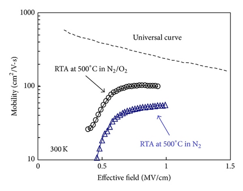
Table 1 lists the capture cross-sections of surface states (σs) at the interface between silicon and oxides, for example, SiO2, ZrO2, Al2O3, CeO2, and HfO2 [22–29]. For SiO2, the σs value is 1–4 × 10⁻¹⁶ cm2 [22–24] which is smaller than those of high-k dielectrics. For CeO2, the σs value is around 9 × 10⁻¹⁵ cm2 even if the adopted measurement method is different [27, 28]. In this work, the experimental results show that the HfO2 films annealed in N2/O2 have lower interface state density (Nit) and higher channel electron mobility (μe) compared to the HfO2 films annealed in N2. Although the different PDA conditions lead to the different values of Nit and μe, the same σs for HfO2 deposited by rf magnetron sputtering is obtained to be around 2.4 × 10⁻¹⁵ cm2. This finding may suggest that the capture cross-section of surface states for some thin film deposition method may be an inherent nature at the interface between silicon and hafnium oxide. It is worthy to note that the capture cross-section of surface states may be influenced by the factors of environment temperature, film thickness, film deposition method, and especially surface preparation of Si substrate prior to HfO2 deposition.
| Oxide material | Capture cross-section | Deposition method | Measurement technique |
|---|---|---|---|
| SiO2 | 1–4 × 10⁻¹⁶ cm2 | Thermal oxidation | Charge pumping [22–24] |
| ZrO2 | 5.8 × 10⁻¹⁶ cm2 | rf sputtering | Gated diode [25] |
| Al2O3 | 1.7 × 10⁻¹⁵ cm2 | PECVD | DLTS [26] |
| CeO2 | 8.7 × 10⁻¹⁵ cm2 | rf sputtering | Gated diode [27] |
| CeO2 | 9.0 × 10⁻¹⁵ cm2 | rf sputtering | Charge pumping [28] |
| HfO2 | 9.4 × 10⁻¹⁵ cm2 | ALD | Charge pumping [29] |
| HfO2 | 2.4 × 10⁻¹⁵ cm2 | rf sputtering | Gated diode (this work) |
- PECVD: plasma-enhanced chemical vapor deposition, DLTS: deep-level transient spectroscopy, and ALD: atomic layer deposition.
4. Conclusions
The electrical properties at the HfO2/Si interface are investigated by the gated-diode method and the subthreshold measurement. Although the HfO2 films annealed in N2/O2 result in lower interface state density and higher channel electron mobility compared to the HfO2 films annealed in N2, the determined surface state capture cross-section at the HfO2/Si interface is the same. This suggests that the surface state capture cross-section may be an inherent nature at the interface between silicon and hafnium oxide.
Conflict of Interests
The author declares that there is no conflict of interests regarding the publication of this paper.
Acknowledgment
The author would like to thank the National Science Council of Taiwan, for supporting this work under Contract no. NSC 102-2221-E-015-MY2.


