Improvement in the Power Conversion Efficiency of Bulk Heterojunction Photovoltaic Device via Thermal Postannealing of Subphthalocyanine:C70 Active Layer
Abstract
The authors report an efficient organic photovoltaic device based on subphthalocyanine (SubPc):C70 bulk heterojunction (BHJ) via the postannealing treatment. The power conversion efficiency is improved from 4.5% to 5.5% due to the increase in short-circuit current density (JSC) from 8.8 to 12.7 mA/cm2 with the expense of decreased fill factor from 52% to 42%. From external quantum efficiency measurements, the spectral shape-independent enhancement over the entire spectrum suggests that the increased JSC mainly originates from improved charge collection efficiency. To confirm this inference, the hole and electron mobilities in the BHJ are estimated from the space-charge limited current, showing improved transport properties at the optimum temperature. Moreover, the morphologic change is also studied as a function of annealing temperature. A larger grain size is observed with increasing temperature due to the phase separation of SubPc and C70. However, at higher temperatures the strong aggregation of C70 molecules may interrupt the pathway of SubPc, resulting in hindered charge transport and, hence, reduced JSC.
1. Introduction
Organic photovoltaic (OPV) devices show great potential for commercialization in this decade, due to the huge progress in power conversion efficiency [1]. In addition, the capability of flexible manufacturing processes promotes the versatility of OPV devices [2]. In principle, OPV devices could be sorted by photoactive material, into polymer-based and small molecular systems [3–5]. A polymer-based OPV device is usually fabricated using the solution process, which enables the blend of the donor and acceptor to form the interpenetrating network for the large dissociation area [5]. With morphological manipulation through the annealing treatment, the phase separation of donor and acceptor can be controlled to enhance the extraction of photocurrent [6, 7]. Thus, high power conversion efficiencies (PCEs) of more than 6% have been reported extensively in the recent years [8–11]. In contrast, the efficiency of small molecule OPV devices is much lower compared with their polymeric counterparts, particularly with regard to the short-circuit current density (JSC), due to the smaller interfacial area between the donor and acceptor in the planar heterojunction, usually seen in thermal evaporation systems [12–14]. Therefore, employing bulk heterojunction in small molecular OPV devices is required for high performance of the devices.
Several research works have successfully shown significant improvement in photocurrent with the bulk heterojunction structure using conventional donors [15–18]. Moreover, the annealing treatment is also extensively performed to enhance the efficiency of the device. Peumans and his coworkers suggested that the phase separation between donor and acceptor could be controlled under the annealing treatment [19]. Sakai and his colleagues observed the considerable increase in all operating parameters in bulk heterojunction devices after the annealing treatment [20]. They attributed the enhancement to the improved charge transport property due to the increased molecular packing density. Wei et al. identified the high dependence of the annealing process on the device performance [21]. Upon increasing the annealing temperature, the JSC can be enhanced by about 20%, leading to higher performance. Wagner et al. studied the morphology as a function of annealing temperature [22]. They found clear phase separation of the mixing layer during the annealing process. The previous research works have shown the potential use of bulk heterojunction in small molecule OPV devices and the additional annealing treatment necessary to achieve a highly efficient device. In this text, we have fabricated a highly efficient bulk heterojunction OPV device by using the postannealing treatment. Due to the phase separation of donor and acceptor during the annealing process, the carrier mobility could be significantly improved and lead to enhanced photocurrent. The morphological change in thin films with different annealing temperatures further confirms the origin of the increased carrier mobility due to the emergence of the larger grains as the temperature increases.
2. Experimental Methods
The device structure used in this report, as shown in Figure 1, is indium tin oxide (ITO)/subphthalocyanine (SubPc):C70 in 1 : 2 weight ratio (50 nm)/tris(4-hydroxy-8-methyl-1,5-naphthyridinate) aluminium (AlmND3) (10 nm)/Al, where AlmND3 serves as buffer layer [23]. Such an optimal mixed ratio of the active layer is thoroughly studied in other works. The ITO substrates were cleaned by solvent sonication and surface subjected to treatment with oxygen plasma prior to use. The deposition of organic and metal layers was done in a high vacuum (8 × 10⁻⁶ Torr) chamber. Before the deposition of buffer layer, the samples were heated on a home-made holder at four temperatures: 50°C, 80°C, 110°C, and 140°C. The devices were completed with deposition of Al through a shadow mask to define the active area of 0.04 cm2 and well encapsulated to isolate ambient influences. Device performance was assessed in open air. The current density-voltage (J-V) characteristics in the dark and under air mass (AM) 1.5 G solar illumination from a solar simulator (Newport 91160A) were determined using a source meter (Keithley 2400). The intensity of solar illumination was calibrated with Si reference cell (PV measurement, area: 3.981 cm2). For the external quantum efficiency (EQE) measurement, a monochromator (Newport 74100) was used to select the wavelength from 350 to 800 nm. The photocurrent from the devices upon illumination was collected using a lock-in amplifier (Signal Recovery 7265), which was chopped at 250 Hz with a chopper. The mobility of holes and electrons with different temperature treatment was estimated from the space-charge limited current (SCLC) with hole- and electron-only devices. The atomic force microscopic (AFM) images were taken with a Park System XE-100 using the noncontact mode and cantilever frequency of 320 kHz.

3. Results and Discussion
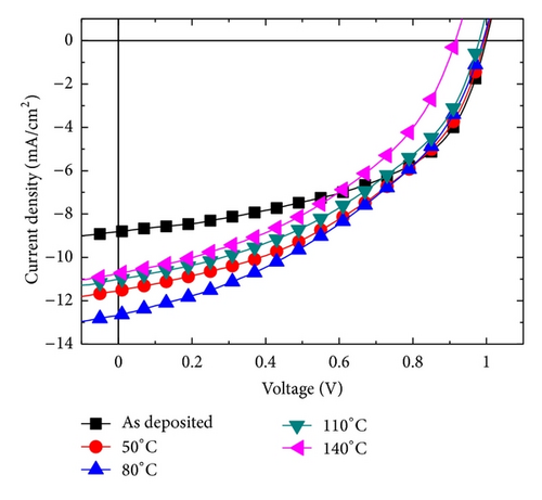
Figure 2 shows the J-V characteristics of the OPV devices with different annealing treatments under AM 1.5 G solar illumination. The photovoltaic parameters are summarized in Table 1. For the device annealed at 140°C, the VOC is significantly decreased to 0.92 V compared with the other devices, which registered about 1 V. The JSC is enhanced from 8.8 to 12.7 mA/cm2 and then reduced to 10.7 mA/cm2 as the annealing temperature increases. The device without treatment shows the highest FF at 52%, while this is considerably decreased after the annealing process. Consequently, the highest PCE of 5.5% is obtained when using the 80°C annealing due to the substantial enhancement in JSC, which is similar to the polymeric system [24, 25]. This is attributed to the critical balance between the phase separation and the charge collection efficiency. The temperature-dependent VOC was also observed in the previous results, which explained this phenomenon using the AFM images [26]. The formation of the island-like morphology at high temperatures due to a high degree of phase separation may cause the enhanced recombination at opposing electric fields, leading to the reduced built-in potential and, hence, the VOC. As a result, temperature annealing tends to increase the phase separation in the mixed layer, leading to the decrease in VOC with temperature.
| Device | V OC (V) | J SC (mA/cm2) | FF (%) | PCE (%) | μ h (cm2/Vs) | μ e (cm2/Vs) |
|---|---|---|---|---|---|---|
| As deposited | 1.00 | 8.8 | 52 | 4.6 | 5.1 × 10 −8 | 1.1 × 10 −4 |
| 50°C | 0.99 | 11.5 | 45 | 5.1 | 4.2 × 10 −7 | 2.2 × 10 −4 |
| 80°C | 0.99 | 12.7 | 44 | 5.5 | 3.4 × 10 −6 | 3.9 × 10 −4 |
| 110°C | 0.98 | 11.0 | 44 | 4.7 | — | — |
| 140°C | 0.92 | 10.7 | 42 | 4.1 | 2.0 × 10 −8 | 7.9 × 10 −4 |
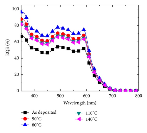
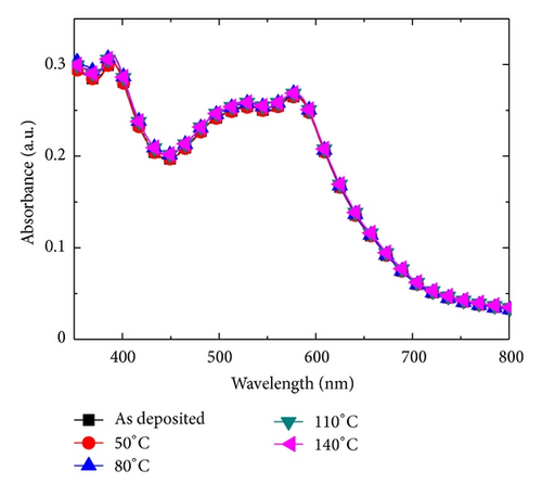
In order to clarify the origin of the significant enhancement in JSC, the EQE is measured as shown in Figure 3(a). The contribution from the absorption property is excluded due to the changeless absorption spectra for all thin films with different annealing temperatures as indicated in Figure 3(b). A large change is observed in EQE over the entire spectrum dependent on the annealing temperature. However, the spectral shape remains the same for all devices. This indicates that the enhanced JSC is mainly due to the improved charge collection efficiency, rather than increased light harvesting from either SubPc or C70, as expected due to the changeless absorption spectra [27, 28]. For most polymeric cases, the postannealing process can improve the crystallinity of the thin film and enhance the carrier mobility [29]. A few studies of OPV devices have shown that better molecular packing during the annealing treatment can lead to increased mobility and, hence, the device performance [21, 30–32]. In our case, the enhanced charge collection efficiency is ascribed to the improved crystallinity after the postannealing. Beyond the optimized temperature, the large phase separation may completely separate the donor and acceptor, resulting in hindered charge transport and a decrease in the JSC.
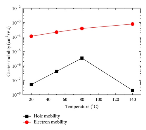
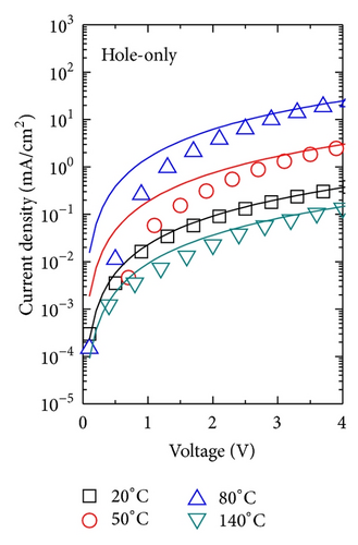
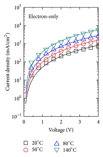
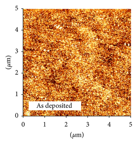
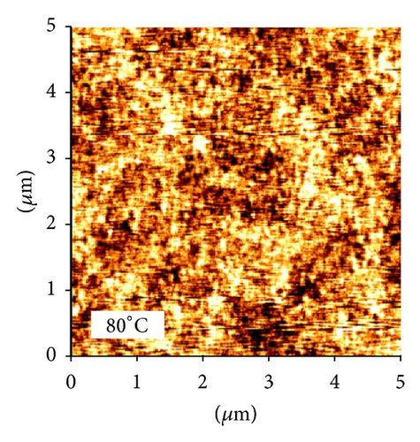
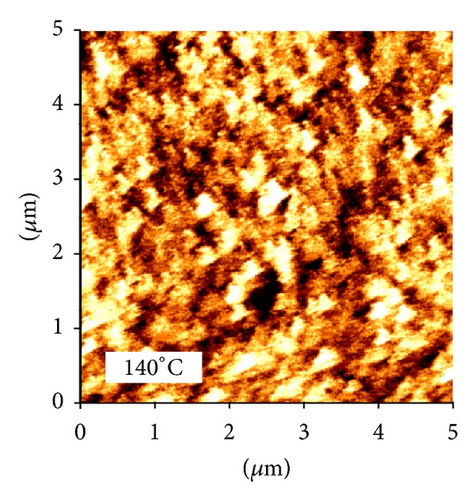
The morphological change because of the annealing temperature is examined by AFM images, as shown in Figure 5. Thin film, as deposited without any treatment, exhibits a rather smooth surface. After performing the annealing at 80°C, the surface of the thin film becomes rougher, indicating that phase separation occurs between the SubPc and C70. When the annealing temperature is 140°C, the larger grains emerge due to the significant phase separation of SubPc and C70. Similar results have been shown in the polymeric systems [25, 41]. Through increasing the annealing temperature, the improved carrier mobility of the hole and electron is ascribed to the enhanced crystallinity of SubPc and C70 within the mixed layer. The high degree of phase aggregation in the 140°C-annealed thin film is attributed to the strong aggregation of C70. From the SCLC measurement, the significant decrease in hole mobility under high temperatures originates from the disconnection of the SubPc pathway. The hindered SubPc pathway is likely due to the strong phase aggregation of C70. Therefore, these results suggest that there is a critical balance between the phase separation and the charge collection efficiency for improved performance of the device.
4. Conclusion
In conclusion, we have demonstrated an efficient OPV device using postannealing treatment. A significant increase in JSC was observed and led to an improved PCE from 4.6% to 5.5%. The spectral shape-dependent increase in EQE over the entire spectrum indicated that the increased JSC came from the improved charge collection efficiency rather than the light harvesting. From the SCLC result, the best charge balance condition as well as the substantial enhancement in carrier mobility at the optimum annealing temperature contributes to the highest photocurrent. Moreover, the effects of annealing on the morphology were also investigated by AFM images. They showed growth of larger-sized grains as the temperature increased, which may be due to the phase separation of SubPc and C70. Therefore, it is believed that the critical tradeoff between the phase separation and charge collection efficiency plays an important role in improving the device performance.
Acknowledgments
The authors acknowledge the Academia Sinica of Taiwan and the financial support from the National Science Council (Grant nos. NSC 102-3113-E-001-001, NSC 101-2221-E-131-025, NSC 101-2627-E-002-005, and NSC 101-2221-E-011-120). In addition, S.-W. Liu specially thanks Mr. Ted Kao, Uchi Optoelectronic (Malaysia) Sdn. Bhd., for the donation of research equipment (Flexible Optoelectronic Device and Processing Laboratory, MCUT).


