A Current Transport Mechanism on the Surface of Pd-SiO2 Mixture for Metal-Semiconductor-Metal GaAs Diodes
Abstract
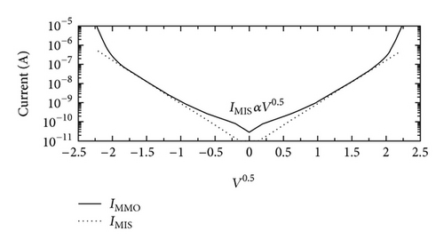
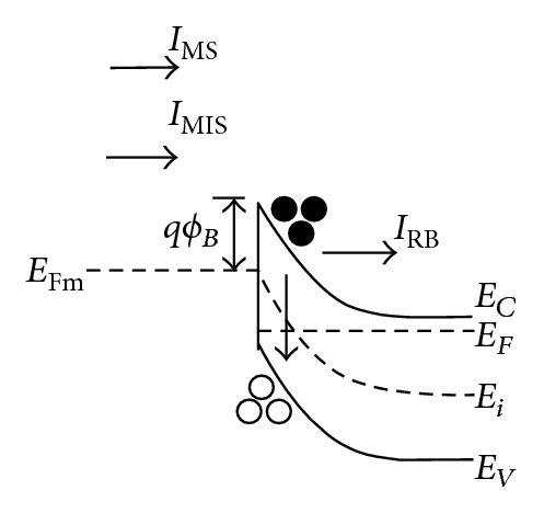
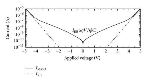
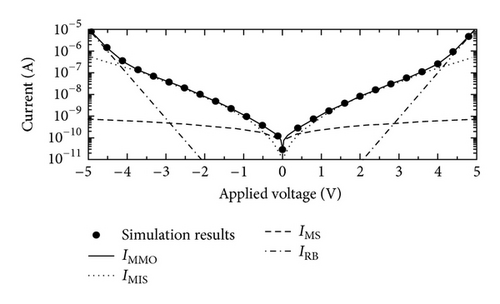
This paper presents a current transport mechanism of Pd metal-semiconductor-metal (MSM) GaAs diodes with a Schottky contact material formed by intentionally mixing SiO2 into a Pd metal. The Schottky emission process, where the thermionic emission both over the metal-semiconductor barrier and over the insulator-semiconductor barrier is considered on the carrier transport of a mixed contact of Pd and SiO2 (MMO) MSM diodes, is analyzed. The image-force lowering is accounted for. In addition, with the applied voltage increased, the carrier recombination is thus considered. The simulation data are presented to explain the experimental results clearly.
1. Introduction
Schottky contact of metal on semiconductor is essential to MESFETs, HEMTs, optical sensors, and gas sensors. Recently, hydrogen has been widely used in hydrogen-fueled vehicles, medical treatment, chemical industries, and semiconductor fabrication. However, hydrogen-containing gases are explosive. Therefore, developing of hydrogen sensors for real-time in situ detection is highly necessary. Previous studies have demonstrated numerous palladium and platinum-based hydrogen sensors [1–14]. Among these sensors, metal-semiconductor (MS) diodes have been addressed as one of the most promising devices [2–7]. Hydrogen sensors employing metal-oxide-semiconductor (MOS) diodes have also been extensively studied [8–10]. In addition, Chiu et al. [11–14] reported a new metal-semiconductor-metal (MSM) hydrogen sensor with two multifinger Schottky contacts. Unlike conventional MS and MOS diodes, a mixture of palladium and silicon dioxides (MMO) is deposited upon the semiconductor layer. Compared to commonly used MS and MOS sensors, the MMO MSM sensors achieve excellent performance of high sensitivity. However, the current-voltage (I-V) characteristics in this paper [14] represent the diode current of the sensor operated in N2. The reason that causes the two-step I-V curve is interesting.
2. Device Structure and Fabrication
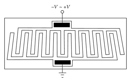
The process started with mesa isolation. HCl was used to remove the native oxide on the 0.8 μm n-GaAs layer with 8 × 1016 cm−3 doping concentration after a device mesa. Two multifinger Schottky electrodes forming a metal-semiconductor-metal (MSM) diode were implemented by thermally depositing a 30 nm mixture of Pd and SiO2 with a weight ratio of 3. The area of the multifinger electrode was A≈ 8 × 10⁻⁴ cm2. Another MSM diode with a 30 nm Pd directly deposited upon the GaAs layer was also fabricated for comparison. Figure 1 shows the MSM diode with two multifinger Schottky contacts.
3. Results Discussion
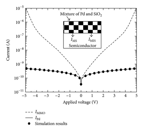
I-V characteristics of MSM diode with and without a mixture of Pd and SiO2 are shown in Figure 2. Because the quality of the epitaxial wafer and evaporative mixture is excellent and uniform, all curves are bidirectional and symmetrical. Unlike the lowest curve representing the current of Pd MSM diodes, the upper curve with the two-step I-V curve is the current of MMO MSM diodes. Obviously, the I-V curve is the same as the published paper [14]; therefore, to deposit a 30 nm mixture of Pd and SiO2 upon the GaAs layer is repeatable.
4. Conclusions
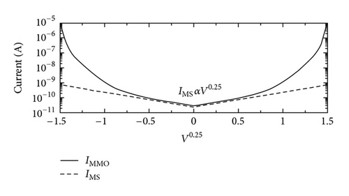
This study examined the current transport mechanism for Pd MSM GaAs diodes with a new Schottky contact material formed by intentionally mixing SiO2 into a Pd metal. A mechanism concept has successfully explained the influence of the mixed SiO2 on the current for MMO MSM diodes under the applied voltage. The effectively simulated data for the Schottky emission process, image-force lowering, and carrier recombination clearly explain the experimental results.
Acknowledgment
This work is financially supported by the National Taiwan Ocean University of the Republic of China under the contract nos. NTOU-100-014 and 101B290031.


