Design a Bioamplifier with High CMRR
Abstract
A CMOS amplifier with differential input and output was designed for very high common-mode rejection ratio (CMRR) and low offset. This design was implemented by the 0.35 μm CMOS technology provided by TSMC. With three stages of amplification and by balanced self-bias, a voltage gain of 80 dB with a CMRR of 130 dB was achieved. The related input offset was as low as 0.6 μV. In addition, the bias circuits were designed to be less sensitive to the power supply. It was expected that the whole amplifier was then more independent of process variations. This fact was confirmed in this study by simulation. With the simulation results, it is promising to exhibit an amplifier with high performances for biomedical applications.
1. Introduction
For biomedical applications, a voltage amplifier with a gain of 80 dB and a high CMRR is required as a building block in front-end subsystems [1, 2]. Since the voltage level of physiologic signals at the front-end subsystem is very weak, processes for analog signals usually include several steps of amplification, filtering, offset adjustment, and electrical conditioning. After suitable processing, the signal will then be large enough and effectively suitable for analog-to-digital conversion at later stages [3–5].
In considering the physiological signals extracted from human bodies, the amplitude of an electrocardiographic (ECG) signal is usually less than 100 μV. Such value is very weak as compared to the noise floor and imperfection of the commonly used operational amplifiers (OPAs). An instrumentation amplifier (IA) is usually employed to achieve the required performances.
In addition to the requirement of high voltage gain in constructing the amplifiers for an IA, another important requirement for the amplifiers is CMRR. According to the recommendations of Association of the Advancement of Medical Instrumentation (AAMI), CMRR is required to be higher than 90 dB with the open-loop voltage gain higher than 80 dB.
In this study, the 0.35 μm CMOS technology of TSMC was employed in designing a high performance amplifier.
In our study, a high-voltage-gain amplifier was tried with a self-biasing technique to have a high CMRR and low input offset and to be less sensitive to process variations. The simulation was performed based on the models supported by Chip Implementation Center (CIC). The related results will be illustrated.
2. Design Details
2.1. Design of the Differential Amplifier
For the purposes of high CMRR and low offset at the input, differential configuration with a symmetrical floor planning in layout will be preferred in the design of an amplifier.
Figure 1 shows the schematic of an amplifier with the differential configuration both at the input and at the output. In this circuit, transistors M1 and M2 are the differential pair for amplification. The block with IT and RT forms a tail current bias. The resistors RD1, RD2, RL1, and RL2 are taken as the loads.
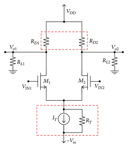
Figure 2 shows an alternative representation of the amplifier in Figure 1. The input and output signals can be decomposed into the common and the differential modes. With this decomposition, the performance of the amplifier in the common mode and the differential mode can be discussed separately.
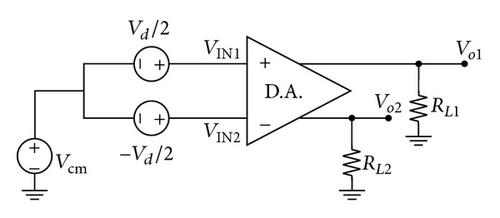
In the common mode, the two output voltages will be the same if the circuit is ideal in a form of total symmetry. This requires that the branches for ID1 and ID2 are matched with RL1 = RL2 and RD1 = RD2.
For the current bias as the tail, a current mirror with a stable reference current, IREF, can be employed in the integrated circuits to give a high output resistance, RT.
Other techniques to improve the performance of this amplifier will be discussed in detail in the following.
2.2. Tristage Amplifier
In this design, three stages of amplification were employed to achieve the required voltage gain and CMRR at the same time for weak biosignals. Figure 3 shows the detailed circuit in this design. Table 1 gives the specifications for this design.
| Parameter | Spec. | Value |
|---|---|---|
| Vo/Vi | ≧ | 20 kV/V |
| AVO | ≧ | 80 dB |
| PM | ≧ | 60° |
| UGF | ≦ | 2 MHz |
| CMRR | ≧ | 90 dB |
| PD | ≦ | 1 mW |
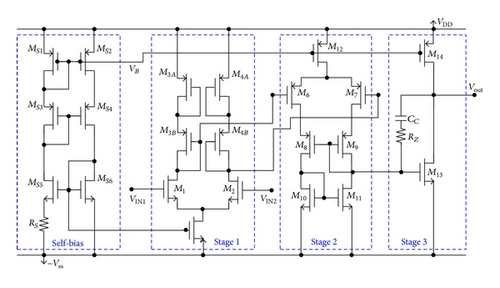
As seen in Figure 3, the first stage is composed of M1–M5. The second stage includes M6–M12. These two stages can be used as an operational transconductance amplifier (OTA) [6, 7] or a folded cascade amplifier [8]. The third stage comprising M13 and M14 forms a type A common-source (CS) amplifier to drive loads.
Transistors MS1–MS6 provide a bias current for the first-stage amplifier. The source of biasing for the second-stage amplifier comes from the balanced self-bias current mirror, M8–M11, in Figure 3. In this part, the biasing currents were less sensitive to the level of the power supply. In addition, the complementary arrangement of the loads at the first-stage and the second-stage amplifiers would reduce the variation of the amplification if there are changes in the NMOS and PMOS. The bias voltage for the third stage comes from M9 in the second stage. Since the bias currents in M9 and M11 were constant, the gate bias for M13 would be constant. Therefore, the properties of the whole amplifier would be less affected by the uncertainties in fabrication.
For the design strategy, the first stage was designed to achieve a high CMRR rather than a high voltage gain. The overall voltage gain was boosted at the second and the third stages. Since this amplifier was designed for biomedical applications, the voltage gain was tried to be as high as possible with a moderate small bandwidth around 100 Hz. At the third stage, a clamping circuit can keep dynamic tracking of the output gain such that the voltage gain would be less affected by variations in the transistors.
In addition to the electrical considerations, the layout and circuit for the first and second stages were designed as symmetrical as possible. In this way, the common signals would be cancelled out in the differential structure. Therefore, the equivalent input offset would be suppressed effectively.
With the above techniques, an amplifier with high voltage gain, high CMRR, low offset, and low drift voltage can be achieved and confirmed in the simulation.
2.3. Transistor Dimensions
In general, the tail current was required to be higher than the product of the screw rate and CC. In this study, this product was 10 μA for the second stage. Since the screw rate for the case of light loads is not required strictly, the tail current at stage 2 was selected as 15 μA.
The bias currents for the two branches through M6 and M7 equally divide the tail current into ID6 = ID8 = ID10 = ID7 = ID9 = ID11 = 7.5 μA.
For the third stage, its transconductance gain, Gm3, is the same as gm13 of M13. We chose Gm3 ≥ 10Gm2; that is, Gm3 ≥ 590 μA/V and gm13 = Gm3 = 600 μA/V. In addition, the overdrive voltage for M13 was selected as VOV13 = 0.2 V; that is, VGS13 ≡ VOV13 + Vtn = 0.85 V. Therefore, VDS13 = VDS14 = 1.65 V. The dimension ratio for (W/L)13 can be determined by (6).
3. Simulation and Verification before Fabrication
In this study, HSPICE with the device models for 0.35 μm CMOS technology from TSMC was employed for the simulation and analysis. The performance of the whole circuit was verified first in the prelayout simulation. Then, the physical layout was implemented and the related parameters were extracted. With the obtained information of the physical layout, the postlayout simulation was performed to check the feasibility of our layout. Corner simulations were also performed to check the effect of the process variation on the performance of our amplifier.
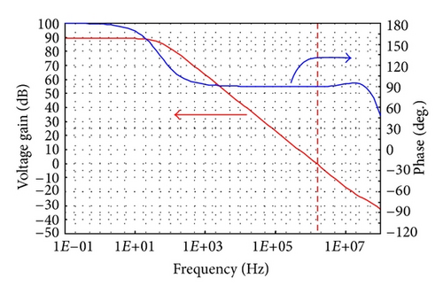
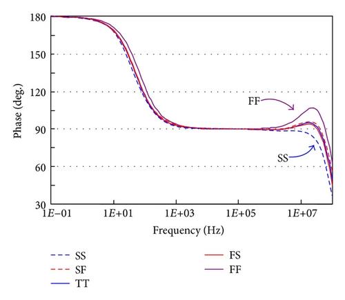
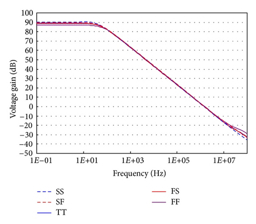
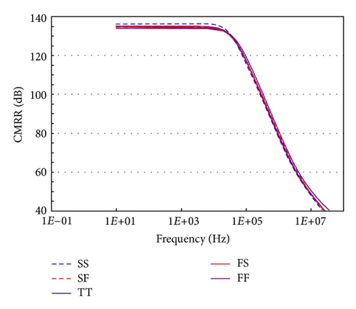
Figures 4–7 illustrate the related performances with 5 corner conditions in fabrication. Table 2 lists other performance items with the 5 corners. With these results, we can find that the voltage gain in Figure 6 can be kept higher than 80 dB. And the variation of the obtained gains due to the uncertainty in fabrication can be smaller than 5 dB. It can also be found in Figures 4 and 5 that the phase margin is much larger than 60°. In Figure 5, we can confirm that the variation of phases is insignificant. As shown in Figure 7, the obtained CMRR is as high as 130 dB for frequency up to 10 kHz. The variation of CMRR due to the fabrication is also insignificant. With these results, a bio-amplifier both with a very high CMRR and a high voltage gain at the same time can be expected for the fabricated chips.
| Items | SS | SF | TT | FS | FF |
|---|---|---|---|---|---|
| Vo/Vi | −33.1 k | −29.7 k | −29.3 k | −27.7 k | −22.6 k |
| AVO (dB) | 90.4 | 89.5 | 89.3 | 88.9 | 87.1 |
| PM | 88.8° | 89.8° | 89.7° | 89.7° | 91.0° |
| fH3db (Hz) | 63.0 | 63.1 | 79.4 | 63.1 | 82 |
| UGF (Hz) | 1.41E + 06 | 1.47E + 06 | 1.46E + 06 | 1.44E + 06 | 1.52E + 06 |
| CMRR (dB) | 136.4351 | 136.2238 | 136.7342 | 136.5733 | 135.778 |
| PD (μW) | 357 | 332 | 328 | 324 | 316 |
| Vos (μV) | 10.8 | 10.1 | 5.2 | 0.033 | 20.8 |
4. Conclusion
A bio-amplifier with high gain and high CMRR was designed and verified in this study. According to the obtained performance properties in Table 2, it is promising that a process independent performance can be obtained for this amplifier.
Acknowledgments
The authors acknowledge the support from Chip Implementation Center (CIC) and Chang Bin Show Chwan Memorial Hospital with the research resources. Partial financial support from National Science Council (NSC), republic of china, is also acknowledged.


