Controlled Fabrication of High-Yield CdS Nanostructures by Compartment Arrangement
Abstract
High-yield, high-purity CdS nanostructures were synthesized in a turf-like configuration using an improved vapor-liquid-solid method. To increase the yield, a compartment arrangement was employed. The specific kind of nanostructure fabricated was found to be directly dependent on the temperature in the compartment. Along with the high-yield growth of CdS nanorods, nanowires, and nanobelts, intertwined structures were also observed, and the electron field emission property of the intertwined structures was investigated and compared with that of other type of nanostructures. Photoluminescence measurements at 10 K showed a peak emission from the CdS nanostructures at 485 nm.
1. Introduction
Nanostructures are considered the critical component in a wide range of potential nanoscale device applications [1–5]. Yet, a procedure to fabricate them with both controllable results and in bulk quantities has to be developed in order to achieve their applications at a reduced cost. Nanomaterials made of CdS, one of the most important II–VI group semiconductors, have been investigated intensively by researchers due to their interesting optoelectronic and physical properties [6]. Among all the explored fabrication techniques [7–9] for making CdS nanostructures, a vapor-liquid-solid (VLS) mechanism has been effectively applied due to its consistency and reliability in CdS nanofabrication. Here, we demonstrate an improved VLS mechanism for bulk, uniform, and controlled growth of different CdS nanoscale structures using a compartment arrangement. These structures could find utilization in chemical sensors [10] or be incorporated into optoelectronic transistors [11].
2. Experiment
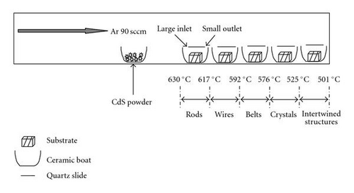
CdS nanostructures were grown in a chemical vapor deposition (CVD) furnace. A clean ceramic boat was partially filled with pure CdS powder (Alfa Aesar, 99.999%) and then placed in the center of a horizontal furnace. 2-mm-thick quartz pieces (cross section ∼1 cm2) were ultrasonically cleaned and then sputter-coated with a gold layer 30 nm thick. Gold was used as the catalyst for nanostructure growth because it is a relatively inert material and will not oxidize either before or during the experiments. These gold-coated substrates were placed in different compartments which were comprised of ceramic boats covered with glass slides. These compartments, arranged closely together, were placed 20 cm from the CdS powder filled ceramic boat. This arrangement is schematically represented in Figure 1.
After the samples had been placed in the furnace, the horizontal tube was evacuated until the pressure was approximately 60 mTorr. Argon gas was then introduced to the chamber, not only as the carrier gas for the CdS vapor, but also to evacuate the impurities in the CVD chamber. The argon was kept constantly flowing at 90 sccm until the pressure inside the quartz tube reached 300 Torr. Then the CVD chamber was slowly heated up at the rate of 20°C/min until it reached the desired growth temperature. This temperature was then maintained for 90 minutes to complete the growth, after which the system was allowed to cool to room temperature. The CdS nanostructures were also uniformly synthesized on the surface of 0.1 mm thick tungsten substrates (Alfa Aesar, 99.95%) using the same procedures described above.
All the samples were characterized by means of the following techniques: an FEI Sirion XL30 field-emission scanning electron microscope (FESEM) was used to study the pretreated catalyst layer and the morphology of the CdS structures; an FEI Tecnai F-20 high-resolution field emission transmission electron microscope (FETEM) was employed to characterize the internal structures of the nanostructures. Electron dispersive X-ray spectrometry (EDX) was used to investigate the chemical composition of the materials. The field emission measurements were performed in an ultra-high vacuum (UHV) chamber at room temperature. The CdS nanostructures were mounted onto the cathode holder of the UHV chamber, which was pumped down to 1 × 10⁻⁹ Torr. A tungsten probe with a 25 μm diameter was used as the anode. The sample was attached to a movable stainless steel plate and connected to a picoammeter for the emission current measurements, while the probe was connected to a high-voltage power supply. Since the cathode plate was connected to a micromanipulator, the position of the nanostructures with respect to the anode probe was variable. During the measurements, the distance between the anode probe and the cathode CdS nanostructures were maintained at a constant distance of 50 μm with the help of an opteron video microscope. Photoluminescence (PL) measurements were performed using a photomultiplier tube (PMT) detector. The 325 nm line from an HeCd laser was used as the excitation source.
3. Results and Discussion
Evidence suggests that there is a close relationship between the size of the gold catalyst and the CdS morphologies; keeping the thickness of the gold catalyst between 25 nm and 30 nm resulted in a higher yield of nanostructures. If the thickness was increased beyond this optimum range, the CdS structures were unable to nucleate [12] because the gold nanospheres became larger and thus denser in size, preventing the CdS vapor from diffusing through the gold.
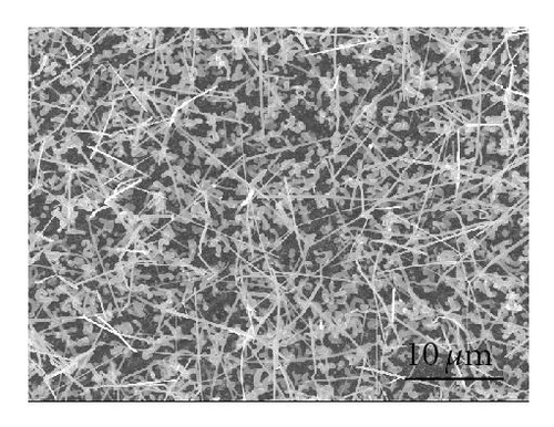
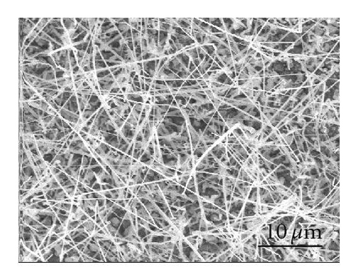
The effect of the compartment arrangement on the yield of CdS nanowires is evident in Figure 2. Figure 2(a) shows growth of CdS nanowires without the compartments; Figure 2(b) demonstrates the much higher yield of CdS nanowires with the compartment arrangement. This compartment arrangement was deployed to trap the CdS vapor at a specific temperature, enabling the growth of CdS nanostructures at a specific temperature and pressure. This is in contrast to the conventional CVD process where most of the CdS vapor is blown away by the carrier gas. This method, using the compartment arrangement as demonstrated in the schematic diagram (Figure 1), allows a specific morphology to be grown on selected substrates.
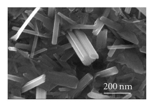
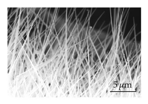
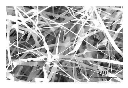
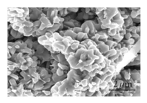
Even though the different CdS nanostructure morphologies depend upon several factors such as pressure, catalyst size, temperature, and flow rate, it has been shown that vapor nucleation is extremely sensitive to temperature and pressure conditions [13], and our study suggests that temperature plays a key role in determining the morphology of the different CdS nanostructures. Therefore, to determine the temperature at different spots inside the CVD furnace, a thermocouple mapping was employed; this clearly showed the specific temperature at which each different nanostructure morphology is formed. CdS nanorods, as seen in Figure 3(a), were found at a temperature range of 617°C–630°C. These nanorods had an average length of 400 nm and a diameter of 120 nm. CdS nanowires, seen in Figure 3(b), formed from 592°C to 617°C; and had an average length of 10 μm and a diameter of 80 nm. CdS nanobelts (see Figure 3(c)) formed between 576°C and 592°C and had an average belt width of 1 μm and a length of 8 μm. Between 525°C and 576°C, small single crystals were formed, as seen in Figure 3(d).
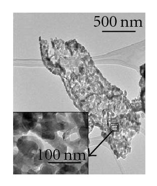
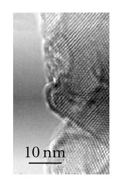
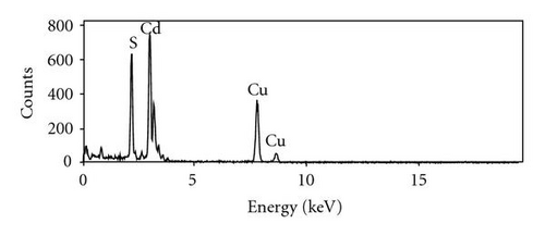
In this investigation, we also observed the growth of CdS intertwined structures, shown in Figure 4(a). These intertwined structures were grown at a relatively lower temperature range, from 525°C to 501°C. Most of the intertwined structures had a diameter of 500 nm; however, as indicated by the inset of Figure 4(a), intertwined CdS nanostructures with a smaller diameter were also formed. Figure 4(b) shows an area of intertwined structures chosen for TEM study, while Figure 4(c) demonstrates the single-crystallinity of the intertwined structures. EDX analysis, as seen in Figure 4(d), suggests that these structures consist of Cd and S. The Cu signal is from the TEM copper grid.

The intertwined structures were chosen for a study of electron field-emission behavior because of their unique structural properties. Even though the intertwined structures do not appear to possess the sharp tips which normally lead to good electron field-emission, we have previously reported field enhancement from rough surfaces [14] and the intertwined structures were found to be similar in appearance to structures shown to have desirable emission characteristics.
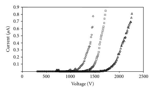
Discussion of these results requires the definition of several parameters. The turn-on and threshold fields of an emitter are defined as the macroscopic external field required to extract a current density of 10 μA/cm2 and 10 mA/cm2, respectively [15]. Current density J is defined as J = I/α. Here, I is the emission current in amperes and α is the emission area of the nanostructures in square centimeters. The emission area was defined as the area of the anode tip [16]; since the same anode was used for every experiment, this definition did not affect the comparison of turn-on and threshold fields.
During the measurement, a tungsten substrate, rather than quartz was chosen to support the CdS intertwined structures as the anode, due to its good conductivity [3]. From Figure 5, it is evident that the cathode surface morphology, and consequently field emission performance, varied throughout the substrate. The results suggest that the intertwined structures on average have turn-on and threshold fields of 13.08 V/μm and 22.05 V/μm, respectively. Both of these numbers are slightly higher than previously reported from CdS nanowires [17], and much higher than that reported from “good” emitters like carbon nanotubes [14]. Because the intertwined structures do not have well-defined tips, their emission characteristics may not be expected to match up with nanowires of similar material.
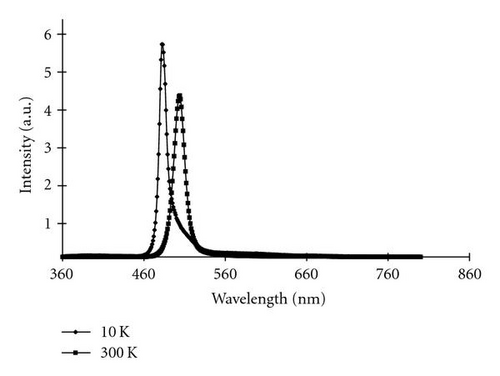
To further understand the optical properties of the CdS nanostructures, PL measurements were performed. At 300 K, the emission spectrum consisted of a sharp peak at 504 nm, while at 10 K, the spectrum consisted of a sharp peak at 485 nm (Figure 6). The given emission spectrum was obtained from CdS nanowires, but the various nanostructures all had similar emission patterns. These emission peaks match the photoluminescence spectra previously reported from CdS nanowires [18]. The 504 nm peak from the measurement performed at 300 K is the near-band-edge emission from CdS; no deep-level defect emissions were observed. When the PL measurements were performed at 10 K, the intensity from the near-band-edge increased, and a blue shift was evident.
In summary, a method which allows the deposition of nanostructures with controlled morphologies in small areas has been demonstrated. Several different high-yield and uniform CdS nanostructure morphologies were grown at specific temperature regions over different substrates using the new compartment arrangement. The TEM analysis verified that these CdS nanostructures, including the intertwined structures, were single-crystalline. The field-emission results of the intertwined structures were comparable to that of previously reported CdS nanowires, and PL measurements confirmed an emission spectrum similar to previously reported spectra from CdS nanowires. It is expected that the new growth method introduced here will allow us to further optimize the growth conditions to advance the development of the controlled fabrication of the nanostructures for specific electronic applications.


