Increased Efficiency of Organic Solar Cells by Seeded Control of the Molecular Morphology in the Active Layer
Abstract
The performance of non-fullerene, polymer bulk heterojunction (BHJ) organic photovoltaic devices has a significant correlation with the molecular morphology of the donor and acceptor. The authors show that small organic molecules coordinated to a metal oxide, an electron transport seed layer (ETSL), can profoundly modify the donor:acceptor molecular morphology of inverted organic photovoltaic (OPV) devices. Using grazing incidence wide angle X-ray scattering (GIWAXS), the authors show that a PTB7-Th:IEICO-4F BHJ active layer has a higher degree of face-on molecular alignment on ETSL-1 (biphenyl-4,4′-dicarboxylic acid, coordinated to ZnO), whilst for naphthalene-2,6-dicarboxylic acid coordinated to ZnO (ETSL-2), it is reduced. Devices of PTB7-Th:IEICO-4F BHJ prepared on ETSL-1 had a 19.91% increase in the average power conversion efficiency (PCE), a 1.56% increase in the fill factor (FF), and a 16.66 ± 0.2% enhancement in the short circuit current density. The observed improvements are believed to be due to significant modifications to the oxide-BHJ interfacial region of ETSL-1, namely the elimination of nano-ridges and defect centers, along with an enhanced wettability. These factors can be correlated with the enhanced device performances, leading to the conclusion that the modulation of the molecular morphology of donor:acceptor blends by ETSL-1 has a broad impact on improving OPV cell efficiencies.
1 Introduction
Nonfullerene small molecule acceptors blended with conjugated polymer semiconductor donors are being extensively studied, largely aimed at improving the efficiency of organic solar cells compatible with wet-chemistry solution processing.[1, 2] To date, nonfullerene acceptor (NFA) materials have received more focus, largely due to significant disadvantages of fullerene acceptor materials, including weak absorption in the visible range, costly synthesis, limited tunability of energy levels, and spherical shape.[3] In contrast, NFAs have easily designed molecular skeletons and flexibility with respect to side-chain functionalization, allowing for tuning of the electronic properties, prerequisites for enhancing organic photovoltaic (OPV) device efficiency.[3] Recent studies have shown that NFA–polymer bulk heterojunctions (BHJs) can result in improved solar cell efficiency when using strategies such as the novel blending of small molecule acceptor–polymer donors, charge transport layer passivation, and solvent-induced BHJ molecular morphological modification.[4-7]
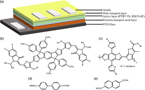
Among all these strategies, very few studies have focused on correlating the heterointerface of the electron charge transport layer and its impact on the molecular morphology of the BHJ to the OPV device performance.[5, 8, 9] For example, NFA–polymer combinations, such as PTB7-Th:ITIC, PTB7-Th:ITIC-4F, and PTB7-Th:IEICO-4F, have regularly been employed in inverted OPV configurations with electron extraction layers (ETLs) such as ZnO and TiO2, but lack a detailed correlation between the ETL and BHJ heterointerface, its effect on the donor:acceptor molecular morphology, and the overall OPV device performance.[5, 8, 9] In addition, controlled reduction of the chemical and physical defects, metal ion vacancy, and surface roughness and uniformity of these aforementioned ETL layers may impact the molecular morphology of the donor:acceptor blends and yet any correlation to the OPV device efficiency is rare to find. Self-assembled monolayers (SAMs) of organic molecules have been found to passivate metal oxide surfaces by greatly reducing the defect centers, but may result in an increase in the interfacial energy barrier, which could reduce the OPV performance.[10-12] Numerous studies have used this approach, including use of the chelating agent ethylenediaminetetraacetic acid (EDTA) on ZnO, fullerene (C60) molecules as a passivation layer on ZnO, while benzoic acid derivatives, tert-butyl amines, and halogenated benzoic acids have also been used as organic linkers on the ETL, all demonstrating some enhancement of the OPV device performance, but lacking in any correlation to the impact on the molecular morphology within the BHJs.[9, 13] One of the most commonly used linkers in coordination chemistry is the deprotonated carboxylic acid group (−COOH), as found in biphenyl-4,4′-dicarboxylic acid (BPDC) and naphthalene-2,6-dicarboxylic acid (NDC). In both of these small organic molecules, the carboxylate groups are oriented at opposite ends of the molecule and as such may act as anchoring sites to bind with the metal oxide surface through surface metal ions (Zn2+) or oxygen defect centers, and may eventually form a flat or tilted thin layers across the metal oxide surface.[14, 15] Studies show that BPDC binds to the surface with one anchoring carboxylate group in an upright or tilted standing orientation, while NDC coordinates to the ZnO surface at both carboxylate groups, resulting in a planar arrangement.[15] Small organic molecules such as benzoic acid, biphenyl-4-carboxylic acid, or terphenyl-4-carboxylic acid on metal oxides may not form highly ordered self-assembled monolayers due to the absence of a second carboxylic acid group which would benefit the formation of intermolecular hydrogen bonds and leading to long-range crystallinity.[16] In the case of BPDC, an upright standing orientation on different metals or metal oxide films is feasible, in which a free carboxylic acid group is retained, facilitating H-bonding and increased crystallinity.[15-17] In addition, enhanced H-bond formation may be feasible between the free carboxylic acid to the fluorine atoms present in either the donors or acceptors of the BHJ.[18] However, in NDC and other planar conjugated phenyl ring systems may display a tendency to form a flat orientation on metal oxides, resulting in a dense long-range self-assembled layer.[15-17] Therefore, BPDC and NDC potentially provide ideal contrasts that allow for a detailed study of the nature of the molecular coordination to the ETL and the impact of the heterointerface on the molecular morphology in the BHJ layer PTB7-Th:IEICO-4F, allowing us to correlate this with the OPV device performance. Here, we have focused primarily on the coordination of the BPDC and on a sol–gel-prepared ZnO film to produce electron transport seed layer-1 (ETSL-1) and compared this to an equivalent ZnO film, electron transport seed layer-2 (ETSL-2), and the capacity of both ETSLs to influence the molecular morphology of a PTB7-Th:IEICO-4F BHJ active layer. We found that ETSL-1 led to a higher face-on molecular order in the PTB7-Th:IEICO-4F layer with a smoother and more uniform surface morphology in addition to a potential templating of the BHJ. ETSL-1 was also found to reduce the interfacial energy barrier between the ETSL lowest unoccupied molecular orbital (LUMO) and the BHJ acceptor state. In contrast, bulk passivation of ETSL-2 was observed due to the agglomerated planar molecular stacking of NDC, reducing the face-on molecular morphology of the PTB7-Th:IEICO-4F BHJ layer. We also observed a high energy offset between the LUMO level of ETSL-2 and the acceptor of the BHJ. The enhanced face-on molecular morphology was highly correlated to the device performances with improved performance in device D1 over D0 and D2. The champion device (glass/ITO/ETSL-1/PTB7-Th:IEICO-4F/MoO3/Ag (D1)) showed a power conversion efficiency (PCE) of 12.53%, with a fill factor (FF) of 65.11%, a short-circuit current density (Jsc) of 26.6 mA cm−2, and open-circuit voltage (Voc) of 0.71 V, compared to 10.74% PCE, 63% FF, 24.35 mA cm−2 Jsc, and 0.69 Voc for the reference device D0 (glass/ITO/ZnO/PTB7-Th:IEICO-4F/MoO3/Ag). An average increase of 19.91% in the PCE of D1 (11.20% up from 9.34%) was recorded compared to D0. Whereas device D2 (glass/ITO/ETSL-2/PTB7-Th:IEICO-4F/MoO3/Ag) showed a reduction of 23.12% in the average PCE (down to 7.18% from 9.34%). Using the same BHJ combination, Xin Song et al. recently reported a higher face-on molecular orientation, improving the average PCE from 9.41% to 12.81% by optimizing the additive concentration.[5] Luye Cao et al. reported OPV devices having PTB7-Th:IEICO-4F as the BHJ showing an average PCE of 11.39%, or 12.72% when using a third component in a ternary system.[19] Jianqiu Wang et al. reported a PCE around 11.13% by optimizing the donor acceptor ratio of PTB7-Th:IEICO-4F.[20] Approaches such as solvent additive concentrations, donor–acceptor ratio optimizations, and third component adding in BHJ could improve the overall device performance for PTB7-Th:IEICO-4F, whereas this ETSL approach could be applied for different nonfullerene polymer donor–acceptor BHJ molecular conformation improvement for enhancing the organic solar cell efficiency.
2 Results and Discussion
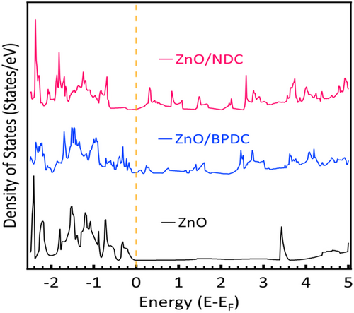
Bader charge analysis was conducted to get more insight into the charge transfer and distribution around the surface of ZnO upon adsorption of BPDC and NDC molecules. It shows higher numerical values of charge distribution for BPDC and NDC in vertical and horizontal orientations on the ZnO surface, respectively (Table S1, Supporting Information). Thus, BPDC favors a vertical geometric attachment upon adsorption on a ZnO surface, whereas NDC attaches horizontally.
An inverted BHJ device configuration was chosen to facilitate the study of the ETSL/BHJ interface in addition for a superior device stability. A sol–gel-prepared ZnO electron extraction layer (30 nm) was treated with BPDC and NDC to generate ETSL-1 and ETSL-2, respectively. The PTB7-Th:IEICO-4F (100 nm) layer was spin-coated on the BPDC/NDC-modified ZnO layer. A MoO3 hole transport layer (HTL, 10 nm) was deposited on the active layer using a shadow mask in a high vacuum thermal evaporator followed by Ag metal layer deposition. The cell area was 0.045 cm2. The schematic of a device is given in Figure 2. The detailed experimental procedure is summarized in Section S1, Supporting Information.
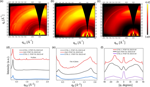
| Film | Peak position [In-plane (100)/out-of-plane (010)] | FWHM | Coherence length [Å] |
|---|---|---|---|
| ZnO/PTB7-Th:IEICO-4F | 0.30 (in-plane) | 0.03 | 186.40 |
| ETSL-1/PTB7-Th:IEICO-4F | 0.30 (in-plane) | 0.05 | 111.84 |
| ETSL-2/PTB7-Th:IEICO-4F | 0.31 (in-plane) | 0.04 | 139.80 |
| ZnO/PTB7-Th:IEICO-4F | 1.77 (out-of-plane) | 0.41 | 13.63 |
| ETSL-1/PTB7-Th:IEICO-4F | 1.81 (out-of-plane) | 0.48 | 11.65 |
| ETSL-2/PTB7-Th:IEICO-4F | 1.82 (out-of-plane) | 1.32 | 4.32 |
The HOF value for ETSL-1/PTB7-Th:IEICO-4F is closest to 1, which relates to the previous observation of the high face-on orientation within the mixed face-on/edge-on molecular morphology. It should be noted that chloronapthalene (CN) was used as additives inside the active layer for all the samples. To optimize the selectivity of the additives, we performed GIWAXS to evaluate the effects of two of the mostly used dopants, chloroform (CF), and CN in the molecular ordering of the PTB7-Th:IEICO-4F BHJ layer. We found a more negative HOF value of −0.06 ± 0.01 for the ETSL-1/PTB7-Th:IEICO-4F (CF additive) (Figure S2, Supporting Information). Thus, CN was found to be a more suitable additive to the PTB7-Th:IEICO-4F BHJ for high face-on molecular order and used for all subsequent samples. The GIWAXS analysis shows that the molecular morphology of the PTB7-Th:IEICO-4F is highly correlated with the ETSL-1 heterointerface. Thus, the interaction of the BPDC/NDC with ZnO is crucial for controlling the PTB7-Th:IEICO-4F molecular morphology.
To understand the surface chemistry of the small organic molecules with the ZnO surface, attenuated total reflectance-Fourier transform infrared (ATR-FTIR) spectroscopy was employed to evaluate the interfacial composition of the ETSL. The out-of-plane deformation mode of the phenyl rings, γoop(CH) at 764 cm−1 (ETSL-2), is polarized perpendicular to the aromatic ring and originates from the planar agglomeration of NDC on the ZnO surface (Figure 4).[14, 15, 17] Meanwhile, the lower intensity of γoop(CH) in ETSL-1 indicates a tilted arrangement of the BPDC to the ZnO surface.[14, 15, 17] The band at 1400 cm−1, which contains contributions from both the OH deformation mode δ(OH) of the free acid and the symmetric OCO stretching mode νs(OCO) of the carboxylate, shows a high intensity in ETSL-2 and a lower intensity in ETSL-1, which may indicate a lower amount of free acid and carboxylate. The high intensity of the ν(CO, stretching) band at 1663 cm−1 is consistent with H-bonded chains of head-to-head coupled NDCs lying flat on the ZnO in ETSL-2. This band has a lower intensity for ETSL-1 due to reduced H-bonding between the molecules.

To further evaluate the BPDC/NDC coordination on the ZnO surface, we employed X-ray photoemission spectroscopy (XPS) to evaluate the ZnO, ETSL-1, and ETSL-2 spectra and determine the corresponding binding energies, allowing us to identify the presence of oxygen vacancies and to correlate it to the coordination properties observed in ATR-FTIR and DFT studies.
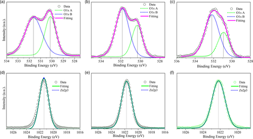
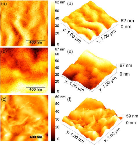
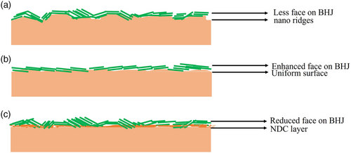
Figure 5 demonstrates the XPS analysis of ZnO, ETSL-1, and ETSL-2. In Figure 5a, two binding energies are observed in the deconvolution of the O 1s region (O 1s B to higher energy and O 1s A ≈1.5 eV lower in energy). The O 1s A peak (530.13 eV, Figure 5a) is associated with oxygen atoms bonded to the nearest Zn atoms in the ZnO lattice, which shifts to 530.32 eV in ETSL-1 (Figure. 5b) due to the interaction between the carboxylate group in BPDC.[27] A much higher binding energy, 530.92 eV, for O 1s A was observed for ETSL-2, indicating an enhanced coordination in NDC/ZnO (Figure 5c), which reflects the extent of bonding between the carboxylate group of the NDC to Zn2+. The O 1s B peak (531.63 eV) relates to the oxygen vacancies or oxygen-deficient regions in ZnO, which shifts to 531.84 eV in ETSL-1 and 532.18 eV in ETSL-2, indicating a stronger interaction with the carboxylate group in ETSL-2 (Figure 5a–c).[28, 29] Overall, the O 1s peaks increase in BE by 0.2 eV between ZnO and ETSL-1 and ≈0.6 eV between ETSL-1 and ETSL-2. Also, the ratio of the relative intensities of O 1s A and O 1s B is 1.5 in ZnO, 1.9 in ETSL-1, and 2.1 in ETSL-2, indicating that oxygen vacancies are more pronounced in ETSL-2 than ETSL-1. The peak at 1021.41 eV (Figure 5d) for the sol–gel-deposited ZnO may originate from the Zn2+ state, which shifts to slightly higher energies in ETSL-1, 1021.71 eV (Figure 5e) and ETSL-2, 1022.17 eV (Figure 5f).[27] Our DFT analysis also shows a similar observation for the BPDC and NDC coordination modes to ZnO. The bandgap energies (Eg) for ZnO, ZnO/BPDC, and ZnO/NDC films were calculated using a Tauc plot (Figure S3, Supporting Information) obtained from their UV–vis absorption spectra (Figure S4g, Supporting Information); a similar bandgap was observed for ZnO and ETSL-1 but a slightly smaller bandgap was observed for ETSL-2. The bandgaps of the ZnO, ETSL-1, and ETSL-2 were 4, 4, and 3.9 eV, respectively, each with an error of ± 0.02 eV (Figure S4, Supporting Information). To evaluate the conduction band (CB) and valence band (VB) positions, we obtained the ultraviolet photoelectron spectra (UPS) of ZnO, ETSL-1, and ETSL-2 films. The cutoff binding energy (Ecutoff) measured (Figure S4a, Supporting Information) for ZnO, ETSL-1, and ETSL-2 films was 17.85, 18.05, and 18.80 eV, respectively, while the Fermi levels (EF) of ZnO, ETSL-1, and ETSL-2 thin films were calculated to be −3.37, −3.17, and −2.42 eV, respectively, using EF = (21.22 eV—Ecutoff).[30] The Fermi edge (EF,edge) was estimated to be around 5.31, 5.31, and 5.28 eV for ZnO, ETSL-1, and ETSL-2 (Figure S4b, Supporting Information), from which the VB was calculated by using the formula VB = (EF—EF,edge).[30] Thus, −8.68, −8.48, and −7.7 eV were the VB values and the CB energies were calculated to be −4.68, −4.48, and −3.8 eV in ZnO, ETSL-1, and ETSL-2, respectively, according to the formula of CB = (VB + Eg).[30] The analysis of the energy levels for all the materials (Figure S4e, Supporting Information) used in this study has shown that the CB energy around −4.48 eV (ETSL-1) is much nearer to the LUMO of the IEICO-4F acceptor (−4.19 eV), which is expected to be significant in reducing interface barrier energy and exciton recombination. Whereas, in case of ETSL-2, a high interfacial barrier energy to PTB7-Th:IEICO-4F BHJ can be seen in Figure S4e, Supporting Information. Thus, an enhanced energy barrier in ETSL-2 does not provide an efficient electron extraction and may reduce device efficiency. Also, strongly agglomerated NDC molecules could abruptly change the wettability with PTB7-Th:IEICO-4F, whereas an optimized smooth heterointerface may occur in the case of ETSL-1. We employed atomic force microscopy (AFM) and contact angle (CA) analysis to measure the surface roughness and the surface energy of the thin films of ZnO, ETSL-1, ETSL-2, and PTB7-Th:IEICO-4F, respectively. Figure 6a shows the surface morphology of the ZnO ETL to be nonuniform and consisting of multiple nanoridges. It should be noted that this nonuniform surface containing nanoridges[31] may not be an optimal interface with an upper BHJ active layer; this may reduce the charge extraction and increase the defect-related recombination properties.[32] Our XPS data also show that the ZnO surface also contains multiple Zn2+ metal ions and oxygen defect zones. The root mean square (RMS) roughness of the ZnO surface was measured to be 23.43 ± 1.5 nm. In contrast, ETSL-1 showed a significant reduction in the nanoridges with a more uniform surface and an RMS roughness of 15.90 ± 1.5 nm (Figure 6b). ETSL-2 by contrast (Figure 6c) displayed an abrupt change in the surface morphology, with an even lower RMS roughness of 5.2 ± 1.5 nm. From Figure 7a, it can be observed that a highly rough ZnO surface with numerous nanoridges may not form an ideal seed layer for the PTB7-Th:IEICO-4F π–π molecular morphology, but ETSL-1 without nanoridges and having a smoother surface (Figure 7b) is an ideal seed layer for a π–π stacked molecular morphology in the BHJ. Thus, the lower surface roughness of ETSL-2 led to an overall decrease in the crystallinity in the BHJ. From the GIWAXS analysis (Figure 3), it was observed that crystallinities of the BHJ are strongly correlated with surface morphologies of the ZnO/ETSL-1/ETSL-2 layers. In case of ETSL-2, a planar and flat orientation of the NDC molecules on ZnO significantly reduces the surface roughness. The flat NDC molecules may have higher interaction with the BHJ, which could negatively impact the crystallinity.[33, 34] Also, this enhanced interaction between the BHJ and the flat-capped NDC molecules of ETSL-2 may reduce donor–acceptor phase separation, along with reduced crystallinities of the BHJ.[10, 35] However, in the case of ETSl-1, a tilted conformation of the BPDC molecules with COOH functional groups could initiate H bonding with the BHJ which would improve its crystallinity.[36] However, a greater face-on morphology is significant for the OPV device performance and was observed in the PTB7-Th:IEICO-4F layer. In addition, a similar surface energy of ETSL-1 with the PTB7-Th:IEICO-4F layer may result in an enhanced heterointerface in comparison to both ZnO and ETSL-2.[10]
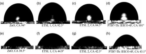
| Sample | Contact angle [water] | Contact angle [diiodomethane] | Surface energy [mN m−1] | Surface energy (polar) [mN m−1] | Surface energy(dispersive) [mN m−1] |
|---|---|---|---|---|---|
| ZnO | 94° | 38.5° | 36.70 | 0.170 | 36.53 |
| ZnO/ETSL-1 | 92.5° | 44.9° | 37.32 | 0.268 | 37.06 |
| ZnO/ETSL-2 | 84.5° | 42.3° | 39.81 | 1.38 | 38.43 |
| PTB7-Th:IEICO-4F | 101° | 43.1° | 38.37 | 0.36 | 38.01 |
2.1 Device Performance
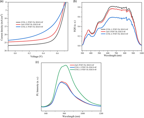
We fabricated three different OPV devices—D0: (glass/ITO/ZnO/PTB7-Th:IEICO-4F/MoO3/Ag), D1: (glass/ITO/ETSL-1/PTB7-Th:IEICO-4F/MoO3/Ag), and D2: (glass/ITO/ETSL-2/PTB-Th:IEICO-4F/MoO3/Ag), with their (J–V) characteristics shown in Figure 9a. D1 showed a high efficiency, with an average of 11.20% PCE (PCE max 12.53%) and an average Voc of 0.70 V and Jsc of 25.2 mA cm−2 and FF of 62.40%, whereas a PCE of 9.34%, 0.66 Voc, 21.80 mA cm−2 Jsc, 61.44% FF were measured for D0. A dramatic lowering of the PCE to around 7.18% PCE, 22.85 mA cm−2 Jsc, and 46.11% FF was measured for D2. Consequently, it can be concluded that the ETSL-1/PTB7-Th:IEICO-4F configuration enhanced the device performance. The averaged data for all the cells (eight cells) is summarized in Table 3. We found that series resistance (RSh) of D2 was much higher than D1 and D0, which suggests less n-type conductivity of the electron extraction layer and a less efficient charge extraction at the interface of the BHJ and the electron extraction layer, consistent with the lower average FF value (Table 3).[27]
| Device | Composition | V oc [V] | J sc [mA cm−2] | FF [%] | PCE [%] | R s [Ω cm2] | R shunt [Ω cm2] |
|---|---|---|---|---|---|---|---|
| D0: aver.best | Glass/ITO/ZnO/PTB7-Th:IEICO-4F/MoO3/Ag | 0.66 (±0.05)0.69 | 21.60 (±0.20)24.35 | 61.44 (±0.15)63 | 9.34 (±0.10) 10.74 | 4.60 (±0.05)5.22 | 500 (±5)637 |
| D1: aver.best | Glass/ITO/ETSL-1/PTB7-Th:IEICO-4F/MoO3/Ag | 0.70 (±0.05)0.71 | 25.2 (±0.2)26.6 | 62.40 (±0.15)65.11 | 11.20 (±0.10)12.53 | 4.55 (±0.05)4.63 | 532 (±5)661 |
|
D2: aver.best |
Glass/ITO/ETSL-2/PTB7-Th:IEICO-4F/MoO3/Ag | 0.71 (±0.05)0.72 | 23 (±0.2)22.85 | 48.10 (±0.15)46.11 | 7.18 (±0.10)7.81 | 10.06 (±0.05)9.86 | 203 (±5)233 |
3 Conclusions
In conclusion, ETSL-1was used as a modified electron extraction layer to control the molecular orientation and crystallization of the PTB7-Th:IEICO-4F BHJ layer. As a result of the controlled molecular order of the BHJ layer and a good interface with ETSL-1, the photon absorption and charge dissociation were improved, which are beneficial for overall device performance. The enhanced device performances were also highly correlated to the increased degree of face-on molecular ordering in the BHJ layer, shown by GIWAXS analysis. In addition, the elimination of multiple surface nanoridges in ETSL-1 played a great role in improving the wettability with the BHJ layer, while the more similar surface energies of ETSL-1 and PTB7-Th:IEICO-4F BHJ made for a more effective interface, lowering the carrier recombination (high shunt resistance) and increasing the PL quenching, giving rise to an increased current density and PCE for device D1 (glass/ITO/ETSL-1/PTB7-Th:IEICO-4F/MoO3/Ag) in comparison to D0 (glass/ITO/ZnO/PTB7-Th:IEICO-4F/MoO3/Ag) and D2 (glass/ITO/ETSL-2/PTB-Th:IEICO-4F/MoO3/Ag). An enhanced average PCE of around 11.20% (PCEmax = 12.53%), 0.7 V Voc, and a Jsc of 25.2 mA cm−2, with an FF of 62.40% were recorded for device D1, whereas D0 showed an average PCE of 9.34%, 0.66 Voc, 21.80 mA cm−2 Jsc, and 61.44% FF. In total, a 19.91% increase in the average PCE, from a reference value of 9.34% to 11.20%, was achieved in D1. By contrast, D2 (glass/ITO/ETSL-2/PTB7-Th:IEICO-4F/MoO3/Ag) showed a reduction of 23.12% in the average PCE (down to 7.18% from the 9.34% reference). The reduction in performance of D2 was correlated to the decreased face-on molecular order in the BHJ, as identified in the GIWAXS analysis. Devices prepared using another nonfullerene acceptor donor (PTB7-Th:ITIC-4F) BHJ layer also showed improved performance when using ETSL-1 compared to bare ZnO. Consequently, this work clearly shows that ETSLs can significantly improve the performance of OPV solar cells by serving as a BHJ molecular ordering modulator.
4 Experimental Section
Materials
The prepatterned ITO glass with an area of 12 × 12 mm was purchased from Lumtec. PTB7-Th, IEICO-4F, and ITIC-4F were purchased from 1-Materials. Zinc acetate dihydrate (Zn(CH3COO)2·2H2O, Sigma-Aldrich, >99.0%), 2-methoxyethanol (CH3OCH2CH2OH, Sigma-Aldrich, 99.8%, anhydrous), ethanolamine (NH2CH2CH2OH, Sigma-Aldrich, >99.5%), 1-chloronaphthalene (CN), biphenyl-4,4′-dicarboxylic acid (C14H10O4, 99%), naphthalene-2,6-dicarboxylic acid (C12H8O4, 99 %), CF, and MoO3 were purchased from Sigma-Aldrich.
Device Fabrication
An inverted device structure of ITO glass/ZnO/PTB7-Th:IEICO-4F/MoO3/Ag (reference device) was used in the study, with slight modification based on our previous studies.[41] The ITO glass substrate was cleaned with soapy deionized (DI) water, pure DI water, acetone, and isopropanol after an ultrasonication for 10 min in sequence. A 0.4 m sol–gel ZnO solution was prepared by dissolving zinc acetate dihydrate (Zn(CH3COO)2·2H2O, Sigma-Aldrich, >99.0%) in 2-methoxyethanol (CH3OCH2CH2OH, Sigma-Aldrich, 99.8%, anhydrous) with an additive ethanolamine (NH2CH2CH2OH, Sigma-Aldrich, >99.5%) and kept at 250 rpm stirring inside the glove box for 12 h. PTB7-Th (10 mg) and IEICO-4F (15 mg) in a 1:1.5 wt ratio in a 25 mg mL−1 chlorobenzene solution with 4 vol% CN were prepared and kept at 200 rpm stirring under a dark condition inside the glove box for 12 h. After stirring, ZnO solution was spin-coated on ITO substrate at 4000 rpm for 60 s. A hot plate air annealing at 170 °C for 40 min was applied to the ZnO thin films. Two 18.5 mM solution of DMF, biphenyl-4,4′-dicarboxylic acid (compound A) and DMF, naphthalene-2,6-dicarboxylic acid (compound B) were prepared after an ultrasonication of 1 h, 30 min heat treatment at 120 °C inside the glove box. Compound A was spin-coated on the ZnO thin film by spin coating at 3000 rpm for 40 s and kept at room temperature conditions for 10 min inside the glove box for ETSL-1 layer preparation. Compound B was also spin-coated on the ZnO thin film by following the exact conditions for ETSL-2 preparation. The stirred active layer solution inside the N2-filled glove box was spin-coated at a rate of 2800 rpm for 1 min onto three kinds of samples (ZnO, ZnO:/ETSL-1, and ZnO/ETSL-2) on ITO glass substrate to reach 100 nm thickness. Right after that, the coated samples were put into a vacuum chamber at a pressure of 10−5 Pa. The 10 nm-thick film of MoO3 and 100 nm-thick film of silver were deposited on the sample surface through a shadow mask by thermal evaporation. All the fabrication steps excluding the BPDC and NDC spin coating here in this report were followed from our previous publication with little modification.[41] The recipe for sol–gel-prepared ZnO usually provides an average 30–40 nm-thick layer, whereas the PTB7-Th: IEICIO-4F BHJ with 1:1.6 in CB gives around 100 nm. We focused for optimizing the spin coater RPM speed of BPDC and NDC on ZnO which was found to be more straightforward way to control the thickness. The device area fabricated was 0.045 cm2. Devices for PTB7-Th:ITIC-4F were also prepared in the same manner with the 1:1.5 D/A ratio with 0.4 vol% CN additive and coated on ZnO and ZnO/BPDC with MoO3 HTL (10 nm) and Ag (100 nm) layer formation.
Device Characterization
The current density–voltage (J–V) measurements were conducted by using a solar cell I–V testing system from PV Measurements, Inc. (using a Keithley 2400 source meter) under illumination power of 100 mW cm2 by an AM1.5 G solar simulator. The device temperature was measured by a GM1350 50:1 LCD infrared thermometer digital gun and maintained at around 25°C. GIWAXS analysis was done at the SAXS/WAXS beamline of the Australian Synchrotron, a part of ANSTO. All the films were deposited on ITO substrates. A Pilatus detector was placed at ≈628.85 mm from the sample position with 13.003 keV X-rays used to give a q-range out to 2 Å−1. The sample to detector distance was fixed at 628.859 mm which has been kept same for all the samples for a q range 0.2–2 Å−1. We used (q = 4π sin(2θ/2)/lambda), where 2θ is the scattering angle, and lambda denotes the X-ray wavelength (0.9537 Å) for calculating the length of the scattering vector q range which depends on the sample to detector distance. The detector pixel size was 0.172 mm. The sample-to-detector distance and X-ray wavelength were calibrated by silver behenate standard. Several angular steps of 0.01–0.05° were taken near the critical angle of 0.15° to have a higher scattering intensity for bulk of the active layer film for each sample, which was determined as the angle of maximum scattered intensity. We used Igor Pro software, Nika macros, SAS 2D for the data reduction. Several steps such as masking, beam center refinement, and sector analysis were performed sequentially applied to generate and correct the 2D pattern and 1D line profiles. GIWAXS sample alignment was done based on the detector to sample position for enabling the sufficient recording of X-ray scattering at wide angles, at (λ = 0.9537 Å) a particular wavelength for several incident angle of the light beam. A vertical and horizontal movement of the detector required for the sample alignment and the selective positioning of the scattering pattern on the detector. An attenuated Fourier transform infrared spectroscopy (Perkin Elmer) was used to study thin films vibrational properties. The X-ray photoelectron spectroscopy (XPS) and UPS were analyzed by ESCALAB250Xi instrument (Thermo Scientific, UK), with an X-ray source of monochromated Al Kα (energy 1486.68 eV) at 160 W (14.5 × 11 mA). A Bruker Dimension ICON SPM with a scan size of “5 mm × 5 mm” at a scan rate of 0.512 Hz was used as the AFM to characterize the film surface morphology. The CA was measured by a CA goniometer using an optical subsystem to capture the profile of DI water (polar) and diiodomethane (nonpolar) (5 μL) droplet on thin films for calculating the surface energies. All the CAs were measured at room temperature within the first 30 s of depositing the droplets (water, diiodomethane) on the thin film surface. A QEX10 spectral response system from PV measurements was used as a characterization machine for highly sensitive EQE measurements. Optical characterization was conducted using a UV–vis–NIR spectrometer (Perkin Elmer-Lambda 950). The PL characterization was conducted using a pulsed OPO laser at 328 nm. For steady-state spectral PL, the signal was detected by a Glacier X TE Cooled CCD spectrometer with a detection range of 200–1050 nm.
Acknowledgements
The authors would like to highly express their sincere gratitude to Australian Nuclear Science and Technology Organization (ANSTO) and Dr. Valerie Mitchell for helping with the GIWAXS experiment. This research was undertaken on the SAXS/WAXS beamline at the Australian Synchrotron, part of ANSTO. The authors would also like to gratefully acknowledge the support from the staff of the School of Photovoltaic and Renewable Energy Engineering (SPREE), Dr. Yin Yao from the Electron Microscope Unit (EMU), and Dr. Anne Rich and Dr. Bill Bin Gong from surface analysis laboratory, Solid State and Elemental Analysis Unit (SSEAU) under Mark Wainwright Analytical Centre, University of New South Wales (UNSW). This work was also undertaken with the assistance of resources and services from the National Computational Infrastructure (NCI), which is supported by the Australian Government, and through the UNSW-NCI partner trial scheme.
Open access publishing facilitated by University of New South Wales, as part of the Wiley - University of New South Wales agreement via the Council of Australian University Librarians.
Conflict of Interest
The authors declare no conflict of interest.
Open Research
Data Availability Statement
The data that support the findings of this study are available from the corresponding author upon reasonable request.


