Extending the Absorption Limit of BiVO4 Photoanodes with Hydrogen Sulfide Treatment
Abstract
Bismuth vanadate is a promising photoanode material for photoelectrochemical water splitting due to its relative stability, low cost, and nontoxic properties. However, its performance is limited by the large bandgap (Eg) of 2.4 eV, and the record photocurrent is already within 90% of its theoretical limit. Further photocurrent enhancement could only be obtained by increasing its optical absorption, for example, by reducing Eg. Herein, sulfur-incorporated bismuth vanadate (S-BiVO4) thin films are synthesized via spray pyrolysis combined with post-treatment in hydrogen sulfide environment. Under optimal H2S treatment conditions, sulfur can be incorporated successfully into the BiVO4 lattice, without the formation of any secondary phases. The use of reactive H2S, instead of solid sulfur powders, allows us to decrease the required annealing temperature and increase the kinetics for sulfur incorporation into BiVO4. The Eg of the resulting S-BiVO4 films is decreased by >200 meV (vs. pristine BiVO4), which theoretically corresponds to a 20% increase in the theoretical photocurrent limit. Finally, the stability limitation of S-BiVO4 is overcome by introducing pulsed-laser-deposited NiOx protection layers. The modified S-BiVO4/ NiOx film exhibits higher photocurrent density with no reduction of photocurrent during the 9 h stability test with AM1.5 illumination.
1 Introduction
The generation of hydrogen via photoelectrochemical (PEC) water splitting is among the promising approaches to fulfil the energy transition toward renewables.[1, 2] The process uses semiconductors with suitable band-edge positions as photoelectrodes.[3] These semiconductors should also ideally be low cost, nontoxic, and stable when immersed in aqueous solutions. Mechanistically, when the semiconductor is illuminated with light, the photogenerated charge carriers, that is, electrons and holes, participate in the reduction and oxidation half reactions at the cathode and anode, respectively.[4] Water oxidation with its four-proton-coupled electron transfer pathway is kinetically the more difficult of the half reactions; more focus has therefore been placed on the fabrication of highly efficient photoanode materials. To this end, due to the high defect tolerance,[5] BiVO4 has emerged as an interesting and exciting photoanode material. BiVO4 photoanodes with photocurrents reaching ≈90% of the theoretical maximum have been reported, and PEC water-splitting devices based on BiVO4 already demonstrate solar-to-hydrogen (STH) efficiencies as high as ≈8%.[6, 7] The current performance is therefore limited by its relatively wide bandgap of 2.4–2.5 eV.[8]
To increase the photocurrent further, the optical absorption of BiVO4 needs to be extended. The valence band maximum (VBM) of BiVO4 is mainly composed of O 2p orbitals and the conduction band minimum (CBM) consists of mainly V 3d orbitals.[9, 10] Therefore, the bandgap of BiVO4 can be modified in two ways: 1) an upward shift of the VBM by an appropriate anion substitution or 2) a downward shift of the CBM by suitable cation substitution. As the CBM is already positioned close to the water reduction potential, the more appropriate approach is to shift the VBM. Efforts on tuning the valence band position of BiVO4 by nitrogen incorporation have been reported, but only minimal band gap reduction was demonstrated.[8, 11] On the other hand, sulfur incorporation results in a bandgap reduction of ≈0.3 eV as well as enhanced charge carrier dynamics.[12] Similar effects have also been reported in other sulfur-incorporated metal oxides (e.g., TiO2, WO3, Fe2O3, CsTaWO6).[13-17] However, in the case of sulfur-incorporated BiVO4, PEC measurements oxidized the sample and sulfur atoms leached out from the BiVO4 films. As a result, the improved optoelectronic properties with sulfur incorporation could not be translated into higher PEC performance.
To overcome the stability limitation, a protection layer is required that inhibits the direct exposure of the film to the electrolyte.[18, 19] This approach has indeed been reported for various metal sulfides.[20, 21] Among the many materials used as protection layers, NiOx is promising to be used on photoanodes due to its p-type characteristic, optical transparency due to the wide bandgap >3 eV, and high stability.[18, 22, 23] It also has relatively good catalytic activity for water oxidation, which means that it can serve both as a protection layer[24] and a cocatalyst. Here, we deposit a thin NiOx layer using pulsed laser deposition (PLD) on sulfur-incorporated BiVO4 films to address the instability issue. As a result, a stable AM1.5 photocurrent of ≈1.7 mA cm−2 is demonstrated for 9 h at an applied potential of 1.23 V versus reversible hydrogen electrode (RHE). In addition, in contrast to previous reports,[12] we utilize postdeposition annealing in hydrogen sulfide (H2S) atmosphere in this study to incorporate sulfur into BiVO4 films. This is advantageous versus treatment using, for example, sulfur powder, because the higher reactivity of H2S allows for incorporation at lower temperature with faster kinetics. The optoelectronic properties of these S-BiVO4 films and their tunability will also be discussed.
2 Results and Discussion
A series of sulfur-incorporated bismuth vanadate thin films were first synthesized by spray pyrolysis using a reported procedure,[25] followed by post-deposition annealing in H2S. Figure 1a shows the X-ray diffractograms (XRD) of BiVO4 films that were annealed under 5% H2S/Ar flow for 20 min at different temperatures from 100 to 300 °C. All films show a pure BiVO4 monoclinic phase, matching well with JCPDS Card No. 14-0688, but the film annealed at 300 °C also shows the presence of a Bi2S3 phase. Postdeposition annealing treatments at different concentrations of H2S and for longer durations were also performed, and the phases identified are summarized in Table S1, Supporting Information. We limit our discussions in the manuscript text to films annealed in 5% H2S/Ar in which no Bi2S3 phase segregation is observed. It can be deduced from Table S1, Supporting Information, that sulfur incorporation via H2S treatment is highly sensitive to the reaction temperature.
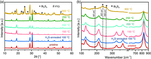
Raman spectra of the films annealed in 5% H2S/Ar for 20 mins were also recorded, which are shown in Figure 1b. For films annealed at 250 °C or lower, vibrational bands at wavenumbers 126, 212, 327, 369, 637, 707, and 827 cm−1 are observed, which can be assigned to the vibrational modes of the monoclinic BiVO4 phase.[26] However, prominent additional peaks at wavenumbers 187, 237, and 260 cm−1 can be observed for the film annealed at 300 °C. These peaks can be attributed to the Bi2S3 phase.[27] This observation agrees very well with the XRD results.
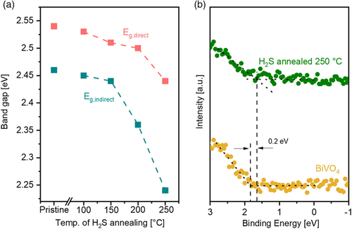
The optical properties of the films were investigated by UV–vis absorption spectroscopy measurements. A redshift of the absorption onset is observed for the H2S-treated samples (Figure S1, Supporting Information). A similar absorption trend is reported in literature for S-incorporated BiVO4 powder by the hydrothermal method.[28] Tauc plots were derived from the absorption spectra to evaluate the bandgap (Figure S2, Supporting Information). The derived bandgaps of all the films are depicted in Figure 2, clearly indicating that the H2S treatment decreases the bandgap of BiVO4 films. A bandgap shift of larger than 200 meV, for the indirect bandgap, is obtained at temperatures higher than 200 °C. Such a bandgap shift corresponds to ≈20% increase in the theoretical AM1.5 photocurrent density limit. This bandgap reduction is confirmed to originate from an upward shift of the VBM upon sulfur incorporation. Figure 2b shows the VB spectra of pristine and H2S-treated BiVO4, measured with hard X-ray photoelectron spectroscopy (HAXPES), using a photon energy of 6 keV (see Experimental Section). Indeed, the VBM of the H2S-treated film is shifted closer to the Fermi level by ≈200 meV as compared with the pristine BiVO4, which agrees very well with the bandgap shift.
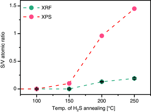
To determine the concentration of sulfur in the films, bulk-sensitive X-ray fluorescence (XRF) and surface-sensitive X-ray photoelectron spectroscopy (XPS) measurements were carried out. Figure 3 depicts the sulfur-to-vanadium (S/V) atomic ratio of the various films, determined from the XRF and XPS data. Both measurements show increasing S/V atomic ratio with increasing H2S annealing temperature. However, the values obtained from XPS are consistently higher than those obtained from XRF. For example, XRF data indicate that the film annealed at 250 °C has an S/V atomic ratio of ≈0.2, but XPS quantification indicates a much higher value of ≈1.5. This suggests that a sulfur gradient exists from the surface to the bulk of the films.
Upon establishing the bandgap reduction and the presence of sulfur in the films, we now proceed to more detailed discussions of the impact of H2S annealing on the properties of BiVO4. From this point onward, we will evaluate and compare the pristine film and the one that underwent postdeposition annealing treatment in 5% H2S/Ar at 250 °C for 20 min; for brevity, these two films will be referred to as “BiVO4” and “S-BiVO4,” respectively.
The chemical nature of BiVO4 and S-BiVO4 films was determined by XPS. As expected, we do not observe any peak in the S 2s core-level spectrum of the BiVO4 film, while the S-BiVO4 film shows a clear presence of a peak (see Figure 4a). The peak for S-BiVO4 can be deconvoluted into two components: one at a binding energy of 225.4 eV (≈83%), which corresponds to S2−, and another component at 227.6 eV (≈17%), which can be attributed to the loosely bound sulfur at the surface.[29] The fact that the majority of sulfur is in the −2 oxidation state further supports that the incorporation of sulfur occurs via the substitution of O2− in the BiVO4 lattice.
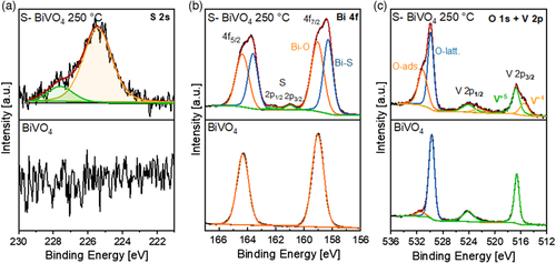
Figure 4b shows the Bi 4f core-level spectra, which consist of peaks with a spin–orbit splitting of 5.3 eV. The peaks are located at the binding energies of 164.3 and 159 eV (labeled as Bi–O) and correspond to Bi 4f5/2 and Bi 4f7/2, respectively.[30] However, the S-BiVO4 film shows additional components at 163.6 and 158.3 eV (labeled as Bi–S). We attribute these peaks to the presence of BiS bonding,[31] although peaks at this binding energy range have also been attributed to reduced Bi.[32-35] The ratio of Bi–O-to-Bi–S peak in the S-BiVO4 film is 1:0.9. Besides this, small peaks can be observed at the binding energies of 162.1 and 160.9 eV. These peaks correspond to S 2p1/2 and 2p3/2 and the position is again in agreement with sulfur being in the −2 oxidation state.[36]
The V 2p core-level spectrum of BiVO4 film shows two peaks due to the spin–orbit splitting (see Figure 4c). The peaks located at the binding energies of 516.6 eV and 524.0 eV correspond to V 2p3/2 and 2p1/2, respectively. These peaks can be fitted each with a single component, showing that V is present in a single oxidation state, that is, +5.[30] However, the V 2p spectrum of S-BiVO4 film can be deconvoluted into two components. Like pristine BiVO4, the peak located at 516.6 eV binding energy can be assigned to +5 oxidation state and the one at 515.4 eV corresponds to +4 oxidation state.[32-35] The ratio of V5+ to V4+ components in the film is 1:0.4. We speculate that this reduction to V4+ is related to the conversion of H2S to S on the surface of BiVO4, as it has indeed been reported that vanadium-based mixed oxide (including BiVO4) acts as a good catalyst for this conversion.[37, 38] In short, a redox reaction takes place between metal oxide and H2S, resulting into the reduction of metal ions (vanadium, in our case) and the oxidation of H2S to S. Figure 4c also shows the O 1s spectrum, being composed of two peaks. The peak at 529.7 eV binding energy corresponds to lattice oxygen (labeled as O-latt.) while the peak at 531.4 eV corresponds to the adsorbates like OH, CO, etc. (labeled as O-ads.).[30] In the case of S-BiVO4 film, the O-ads. peak becomes more pronounced, which may be related to the reduction of V and Bi atoms (see above). Overall, it can be concluded that H2S treatment of the BiVO4 film results in partial reduction of the metal ions along with S incorporation.
We now turn our attention to the effect of H2S treatment on the photoconductivity (ΔG) and charge carrier dynamics of BiVO4. Time-resolved microwave conductivity (TRMC) measurements were performed, and the peak of photoconductivity change (ΔGmax), which is related to the charge carrier mobility, is plotted as a function of the excitation wavelength to generate the photoconductivity action spectra (PCAS) as shown in Figure 5a. For comparison, the values were normalized to the maximum value, which in this case is the value for pristine BiVO4 at 470 nm. While the ΔGmax of S-BiVO4 is significantly lower than that of BiVO4, the PCAS onset for S-BiVO4 is extended to 700 nm versus 520 nm for BiVO4. These onset values match well with the absorption onset, suggesting that sulfur incorporation by H2S treatment has indeed extended the absorption limit as well as the threshold for generating mobile carriers in BiVO4 film. Figure 5b shows the normalized photoconductivity (ΔG/ΔGmax) of BiVO4 and S-BiVO4 film as a function of time. The two curves show the same decay profile, indicating that the lifetime of charge carriers is unaffected by the H2S treatment.
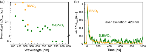
We note that the impact of sulfur incorporation in this study on ΔGmax—which again is a measure of charge carrier mobility—is different compared with our previous study where S-BiVO4 films were obtained via annealing in an S-rich environment (i.e., not H2S).[12] In that case, S-BiVO4 films were shown to possess higher charge carrier mobility than BiVO4 films. Nevertheless, the H2S treatment in the current study is much more effective in extending the photoactivity onset; annealing in an S-rich environment only shifts the onset to ≈580 nm, while annealing in H2S results in an onset shift up to ≈700 nm. We speculate that this variation of photoactivity onset is related to the way that sulfur atoms are configured inside the BiVO4 lattice. Indeed, we have shown in our previous study through density functional theory (DFT) calculations that the configuration of sulfur incorporation (i.e., well-dispersed pairing, around Bi, around V, linear, or random) largely affects the electronic bandgap. At the same time, H2S treatment seems to introduce higher degree of cation reduction in BiVO4 (e.g., from V5+ to V4+) than annealing in an S-rich environment; this may be the reason behind the lower charge carrier mobility. Overall, this suggests that the intricacy of sulfur incorporation and its effect on the electronic structure of BiVO4 is very much dependent on the postannealing environment and the sulfur source.
The PEC properties of the films were characterized by performing chopped linear scan voltammetry (LSV) in 0.1 m potassium phosphate buffer (KPi) at pH 7 under back-side AM1.5 illumination. A photocurrent density of ≈1.1 mA cm−2 at 1.23 V versus RHE was obtained for the S-BiVO4 films (see red curve in Figure 6a). However, the photocurrent decreases in the subsequent LSV cycles (see Figure S3, Supporting Information), suggesting that the films are unstable during PEC measurements. Indeed, chronoamperometric measurements reveal that the photocurrent density decreases from 1.5 to ≈0.4 mA cm−2 within 20 min (see Figure 6b). We attribute this photocurrent decrease to the (photo)electrochemical oxidation of S-BiVO4 film back to BiVO4 and removal of sulfur from the films. This is supported by the observation that the color of the films turns back to yellow after PEC measurement, just like the films prior to H2S treatment (see Figure S4a,b, Supporting Information). Indeed, no sulfur peak can be detected during the XPS measurement of the sample after PEC measurement (see Figure S5, Supporting Information), and the LSV curve shows similar photocurrents to that of non-H2S-treated BiVO4 films (see Figure S6, Supporting Information). Similar behavior has been reported earlier for S-incorporated BiVO4 films and sulfide semiconductors.[12, 21]
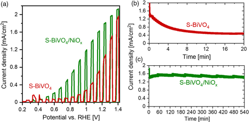
To prevent this unfavored reoxidation and extend the stability of the S-BiVO4 films, we deposited a 20 nm-thick hole-conducting NiOx protection layer using PLD (see Experimental Section for detailed procedures). The PLD process was done at lower oxygen partial pressure in order to prevent the oxidation of S-BiVO4 during deposition. Following the activation of the film (see Figure S7, Supporting Information), as is typical for the nickel oxide-based catalyst,[39, 40] the modified film (S-BiVO4/NiOx) was subjected to the same chopped LSV measurements under AM1.5 illumination. A photocurrent density of ≈1.7 mA cm−2 was obtained at 1.23 V versus RHE (see Figure 6a), which is higher than that obtained with the bare S-BiVO4 film.
More importantly, the NiOx-coated film demonstrates superior stability. Chronoamperometric measurement was performed for 9 h—again, following the activation step—and the photocurrent density remains relatively stable at ≈1.5 mA cm−2 (see Figure 6c). Note that the minor current fluctuations observed after every ≈100 min are caused by the accumulation and release of oxygen bubbles from the surface of the film. No noticeable change is observed in the color of the film before and after PEC measurements (see Figure S4c,d, Supporting Information), indicating that the NiOx protection layer has prevented the reoxidation of the S-BiVO4 film. Chopped LSV measurement after the chronoamperometric measurement also results in no degradation of photocurrent (see Figure S8, Supporting Information). Overall, these results demonstrate that NiOx can act as an effective protection layer for S-BiVO4 photoanodes.
3 Conclusion
In summary, we have incorporated sulfur into BiVO4 films by performing postdeposition annealing under the continuous flow of hydrogen sulfide. Under optimum annealing conditions (temperature, pressure, and time), the formation of a secondary phase (e.g., Bi2S3) can be avoided and sulfur can be largely introduced to substitute oxygen in the lattice of BiVO4. The optical absorption onset of these sulfur-incorporated BiVO4 (S-BiVO4) films is red shifted to 700 nm, which is caused by the upward shift of the VBM, as shown by HAXPES data. TRMC analysis reveals that the photogenerated charge carriers are mobile across the entire absorption range. Stability during PEC conditions is, however, an issue, and we show that the deposition of a NiOx protection layer of ≈20 nm thickness can overcome this limitation. Long-term chronoamperometric measurement (9 h) using a NiOx-coated S-BiVO4 film demonstrates no degradation in the photocurrent. Overall, this study presents a new approach to extend the absorption limit of BiVO4 (i.e., via hydrogen sulfide treatment) and at the same time enhance the stability of the modified photoelectrode.
4 Experimental Section
Synthesis
BiVO4 thin films were synthesized by the spray pyrolysis technique, following the recipe reported in literature.[25, 41, 42] Deposition was carried out onto fluorine-doped tin oxide (FTO)-coated glass substrates (TEC7, Pilkington) and quartz substrates (Spectrosil 2000, Baumbauch & Co. LTD). These substrates were initially cleaned by 10 vol% Triton X-100 solution (Sigma-Aldrich), followed by ultrasonication using acetone, ethanol, and deionized water and dried using N2 stream. The precursor solution was prepared by dissolving 1.2 mmol VO(C2H7O2)2 (99%, Alfa Aesar) and 1.2 mmol Bi(NO3)3.5H2O (98%, Alfa Aesar) in 270 mL solvent consisting of acetic acid (98%, Sigma Aldrich) and ethanol (Sigma Aldrich) in a 1:8 ratio. Prior to BiVO4 deposition, a thin interfacial layer of SnO2 was deposited as a hole blocking layer on the FTO substrates using 5 mL solution of 0.1 m SnCl4 (98%, Sigma Aldrich) in ethyl acetate (99.8%, VWR Chemical).[43] The solution was sprayed using a spray nozzle (Quickmist air atomizing spray, 1/4QMJAU-NC + SUQR-200) onto the substrates, which were placed on a hot plate at 425 °C. A spray cycle consisted of a pulse mode with 5 s spray time followed by 53 s delay for evaporating the solvent. The spray rate was adjusted to 2 mL per cycle. The as-deposited films were then annealed in air at 450 °C for 2 h to form the pristine BiVO4 films.
For sulfur incorporation, the pristine BiVO4 films were annealed in H2S/Ar gas environment (various conc. of H2S: 1–5%) using a tube furnace. The annealing temperature was varied from 100 to 300 °C, and the duration was between 20 and 60 min. A constant ramp rate of 10 °C per min was used.
The NiOx protection layers (20 nm thick) were deposited using PLD.[44, 45] In short, a Ni target (99.99%, Alfa Aesar) was ablated in a custom-built PLD system from PREVAC with a KrF excimer laser with a wavelength of λ = 248 nm (LPXpro 210, Coherent). Target ablation was performed with a repetition rate of 10 Hz and a laser fluence of 2 J cm−2. The target-to-substrate distance was set to 6 cm with the substrate in an off-axis position and the substrate was rotated continuously to get homogeneous film deposition. During deposition, an oxygen background pressure of 5 × 10⁻² mbar was kept in the chamber and the base pressure in the chamber was ≈10−7 mbar. The number of shots was adjusted to obtain the desired film thickness.
Materials Characterization
XRD was recorded using a Bruker D8 diffractometer with Cu Kα radiation (λ = 1.5406 Å). Measurements were carried out at 40 mA and 40 kV in grazing-incidence geometry at an incident angle of 0.5° with a step size of 0.02° and an integration time of 6 s. Raman spectra were measured using a Horiba HR800 spectrometer equipped with a He−Ne laser having an excitation energy of 632.8 nm. UV–vis absorption spectra were recorded in transflectance mode using a PerkinElmer Lambda 950 spectrometer equipped with an integrating sphere. XRF measurements were performed using Bruker M4 Tornado X-Ray Fluorescence Spectrometer with Rh tube having maximal excitation of 50 kV/30 W and SDD detector with an energy resolution of 145 eV. The compositions were then calculated using the Bruker software suite. XPS were carried out using SPECS FOCUS 500 monochromator (Al Kα radiation and hν = 1486.74 eV) and SPECS PHOIBOS 100 electron analyzer. All spectra were referenced with respect to the carbon C 1s peak at 284.8 eV and fitted using XPS PEAK software along with a Shirley background subtraction. The fitted spectra were further optimized by chi-square minimization. For valence band spectra, HAXPES measurements were carried out at BESSY II synchrotron facility (Helmholtz-Zentrum Berlin, Germany) using the HiKE end station at KMC-1 beamline.[46, 47] The photon excitation energy was adjusted to 6009 eV using the higher-order diffracted light from the Si(111) planes of the double-crystal monochromator and the analysis chamber was kept at ≈10−8 mbar. In this measurement, step size and pass energy were set to 0.05 and 200 eV, respectively. The photoelectrons were detected using a Scienta R4000 analyzer. The binding energy scale was referenced to the Au 4f core level (84.0 eV).
TRMC measurements were carried out using BiVO4 and S-BiVO4 film deposited on quartz. During the measurement, the sample was placed in a microwave cavity cell. A voltage-controlled oscillator (SiversIMA VO3262X) was used as the probe to generate a microwave (X-band 8.4–8.7 MHz) and a wavelength-tunable optical parametric oscillator (OPO) coupled to a diode-pumped Q-switched Nd:YAG laser was used as the excitation source. Further details of the TRMC setup and experiment are described in other studies.[48-50]
PEC Analysis
Acknowledgements
The authors would like to acknowledge Deutscher Akademischer Austauschdienst (DAAD) for financial support provided during this work with the funding programme, Research Grants, Binationally Supervised Doctoral Degrees, 2019/20 (funding ID 57440919, personal ref. no 91731054), which allowed the research stay of S.G. at the Helmholtz-Zentrum Berlin. Part of the work described in this paper was conducted within the project SUNCOCHEM. This project received funding from the European Union's Horizon 2020 Research and Innovation programme under grant agreement no. 862192. P.S. acknowledges financial support for this work from the Helmholtz International Research School “Hybrid Integrated Systems for Conversion of Solar Energy” (HI-SCORE), an initiative cofunded by the Initiative and Networking Fund of the Helmholtz Association. The authors thank Christian Höhn for performing the XPS measurements and Roberto Felix Duarte for the access and technical assistance to the HiKE end station, KMC-1 beamline at the BESSY-II synchrotron facility.
Open Access funding enabled and organized by Projekt DEAL.
Conflict of Interest
The authors declare no conflict of interest.
Open Research
Data Availability Statement
The data that support the findings of this study are available from the corresponding author upon reasonable request.


