Charge Separation Efficiency in WO3/BiVO4 Photoanodes with CoFe Prussian Blue Catalyst Studied by Wavelength-Dependent Intensity-Modulated Photocurrent Spectroscopy
Abstract
The understanding of charge carrier dynamics in complex heterojunctions is of the utmost importance for the performance optimization of photoelectrochemical cells, especially in operando. Intensity-modulated photocurrent spectroscopy (IMPS) is a powerful tool to this aim, but the information content provided by this technique can be further enhanced by selectively probing each layer of complex heterojunctions by means of multiple excitation sources. Herein, the charge carrier dynamics of a WO3/BiVO4/CoFe–PB heterojunction, used in a conventional three electrode cell for water splitting, is studied using wavelength-dependent IMPS (WD-IMPS). The proposed data analysis allows us to identify the occurrence of interface recombination processes affecting the semiconductor junction, as well as the positive contribution of the inorganic complex catalyst on the charge separation efficiency of the BiVO4 layer. The deep understanding of the fate of charge carriers in the studied photoanode validates WD-IMPS as a straightforward method to widen the understanding of such structures.
1 Introduction
The conversion of sunlight into fuels represents one of the few sustainable solutions to the ever-growing demand of the energy market, currently undergoing a transition from fossil fuels to renewable energy sources. Among the different processes yielding chemical fuels using solar energy, the photoelectrochemical (PEC) splitting of water into molecular hydrogen and oxygen has a leading role, enabling the storage of intermittent renewable solar energy[1] through clean, waste-free chemistry. Metal oxide semiconductors (MOS) are promising materials to be used in PEC devices because of their good stability, cost-effectiveness, nontoxicity, and light-harvesting properties over the visible spectrum.[2] Due to their deep valence band and the resistance against photocorrosion in oxidative environment, MOS are often used as photoanodes in a tandem PEC configuration to drive the oxygen evolution reaction (OER) in a separated environment.
These materials need to efficiently absorb light, have good bulk transport properties to separate the photogenerated charges, and induce fast charge transfer from the electrode inside the solution to promote the OER, often with the help of surface catalysts.[3-5]
Heterojunctions based on WO3/BiVO4 semiconductors currently represent the state of the art in terms of photoanodes for OER.[6, 7] WO3 is an MOS providing excellent electron mobility and good chemical stability in acidic aqueous solutions, but its wide bandgap (2.7 eV) limits its light harvesting efficiency (LHE) to about 12% of the solar spectrum.[8, 9] On the other hand, BiVO4 is a ternary metal oxide with a narrow bandgap (2.4 eV),[10] but poor charge separation and surface kinetics hinder its PEC performance.[11]
Thus, by building a WO3/BiVO4 heterojunction, WO3 controls the transport properties and enhances the poor charge extraction of BiVO4, by promoting the injection of photogenerated electrons from BiVO4 to WO3 and suppressing bulk recombination. On the other hand, BiVO4 provides enhanced photon collection in the visible region, up to ≈500 nm.[12, 13]
The poor surface kinetics of OER on BiVO4 can be further improved by depositing OER catalyst. Prussian blue (PB)-type materials are promising alternatives to noble metals-based catalysts (Ir or Ru), which are the benchmark for OER catalysis.[14] These inorganic complex salts are easily produced by soft chemistry methods[15] and are stable within a very large pH range.[16] Among them, CoFe–PB showed a remarkable increase in photocurrent, lower photoanodic onset potentials, and excellent stability when coupled with BiVO4.[3]
To further improve the design of PEC devices for solar fuel production, it is necessary to understand the properties and limitations of each material or junction with regard to the key optoelectronic processes, namely, 1) exciton generation upon light absorption, 2) charge separation and bulk transport, 3) charge transfer at the semiconductor–electrolyte interface.
Among various spectroscopic and electrochemical techniques available to explore the dynamics of PEC interfaces, operando techniques are most valuable, because they provide information about the behavior of the system upon external stimuli, such as illumination, applied bias, and chemical environment.
Electrochemical impedance spectroscopy (EIS) is a powerful technique to probe the electrical properties of photoelectrodes in the dark, but, for their characterization under light stimulus, modeling through an electrical equivalent circuit that describes the relevant physical processes occurring within the material is required. In the presence of multiple competing processes and complex interfaces, which are often found in PEC systems, the construction of an electrical model can be difficult, as the frequency response of the PEC system may depend on several interlaced resistive and capacitive contributions, which are sometimes difficult to separate or interpret in an unambiguous fashion. Even though EIS is widely used to study the capacitive response of semiconductor/electrolyte interfaces, the characterization of the relevant kinetic processes occurring at heterojunctions and semiconductor/electrolyte interfaces can be more effectively carried out by intensity-modulated photocurrent spectroscopy (IMPS). The basic idea of IMPS is to analyze, as a function of frequency, the amplitude and phase of the photocurrent generated by the system in response to a sinusoidal modulation of the incident light intensity, which perturbs the surface concentration of the photogenerated carriers.[17-19]
In this work, the charge carrier dynamics of a WO3/BiVO4/CoFe–PB heterojunction, used in a conventional three-electrode cell for water splitting, has been studied using IMPS. To gain a detailed and consistent picture of the processes occurring at such a complex PEC interface, the behavior of WO3/BiVO4/CoFe-PB heterojunction was compared with pristine colloidal WO3 and WO3/BiVO4 heterojunctions with and without the addition of a CoFe–PB catalyst. In particular, after a complete structural and functional characterization of these photoanodes, we applied an innovative approach to investigate the photoinduced carrier dynamics: this technique is based on the implementation of wavelength-dependent IMPS (WD-IMPS) analysis, which selectively probes each different layer of the proposed heterojunction and identifies its electron transport properties in the bulk and at the interface. Thus, this methodology offers the ability to separate and address the role of each active component within a complex interface and represents a valuable tool for improving the understanding of dynamic processes relevant to PEC water splitting.
2 Results and Discussion
2.1 Structure, Morphology, and Optical Properties
Morphological characterization of the photoanodes is reported in Figure 1. Colloidal WO3 (Figure 1a) is characterized by a nanostructured morphology made of aggregated nanoparticles with an average diameter of 45 ± 12 nm, sintered together in a porous 3D network. After the electrodeposition of BiVO4 on WO3 (Figure 1b), a homogeneous thin layer appears on the WO3 nanoparticles, increasing the average size to 52 ± 8 nm. Finally, the addition of CoFe–PB catalyst results in homogeneous coating on top of BiVO4 (Figure 1c). High-resolution transmission electron microscopy (HRTEM) micrographs of the WO3/BiVO4/CoFe–PB heterojunction display crystalline nanoparticles with d-spacing compatible with monoclinic WO3 (Figure 1e,f). Interestingly, the surface of WO3 colloids did not display a homogeneous compact layer of BiVO4 nanoparticles (Figure 1g) but rather small (<10 nm) BiVO4 nanocrystals. While their crystal structure cannot be fully resolved due to beam sensitivity-related instability, the observed interplanar spacings are compatible with distorted scheelite BiVO4. The average composition obtained by energy-dispersive spectrometry (EDS) analysis in scanning electron microscopy (SEM) is reported in Figure S1, Supporting Information, while the local composition and the distribution of CoFe–PB catalyst are further illustrated by the scanning transmission electron microscopy (STEM)–EDS maps in Figure S2, Supporting Information, displaying homogeneous distribution both on BiVO4 and on WO3 layers.
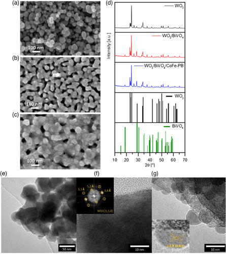
Figure 1d shows the X-Ray diffraction (XRD) profiles of the three photoanodes. In agreement with the above HRTEM analysis, WO3 films exhibit a monoclinic structure, while BiVO4 films show the typical monoclinic clinobisvanite structure (distorted scheelite structure), as previously reported.[20] The WO3 peak intensities are the same in all the photoanodes, and the reflections associated to BiVO4 are much lower in intensity than those corresponding to WO3 due to the different thicknesses of the two layers. The addition of the catalyst does not modify the XRD profile, as expected for a very thin overlayer.
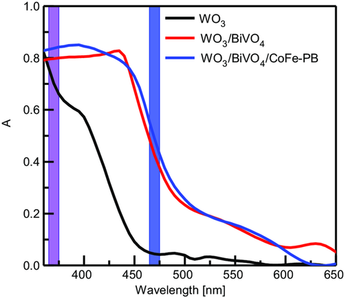
Figure 2 displays the optical absorbance spectra of the WO3 film and of the WO3/BiVO4 heterojunction, with and without the CoFe–PB catalyst. The spectra are in good agreement with the nominal bandgap energies for WO3 and BiVO4, respectively, about 2.7 eV (440 nm) and 2.4 eV (510 nm).[9, 10, 21, 22] The catalyst does not add any significant contributions to the absorption properties of the material in the considered wavelength range. Due to the minor transmittance of the heterostructure in the UV region, the contribution of WO3 to the absorption spectrum was not observed in the corresponding samples, as frequently reported in similar samples.[12]
2.2 PEC Characterization
The electrochemically active surface area (ECSA) of the WO3 film gives an estimation of the real surface area involved in the PEC processes, and it was extracted from EIS data at open-circuit potential (Figure S5, Supporting Information) and from Mott–Schottky measurements (Figure S6, Supporting Information) on the WO3 photoanode in the dark. The ECSA was estimated ≈24 times higher than that of a flat electrode (further details on the calculation are reported in Supporting Information), and therefore WO3 can be considered as mesoporous.[14, 23-25] The addition of BiVO4 and CoFe–PB on the surface of WO3 does not significantly modify the morphology of the photoanode surface, as suggested by SEM and TEM analysis; thus, the whole structure can be considered mesoporous as well.
Figure 3a shows the linear sweep voltammetry (LSV) curves measured in acetate solution under chopped white LED illumination, with an incident intensity of 1 sun. Important contributions of the BiVO4 layer and of the CoFe–PB catalyst can be noticed with respect to bare WO3. The deposition of BiVO4 on colloidal WO3 enhances more than four times the maximum photocurrent (1.85 mA cm−2 at 1.7 VRHE) and shifts the onset toward more positive potentials, requiring a stronger anodic polarization to reach the saturation photocurrent. The deposition of CoFe–PB on top of the heterojunction further increases the photocurrent density, up to almost 2.5 mA cm−2. Moreover, the onset is shifted back to more cathodic potentials, approaching the one observed in pristine WO3, as already reported in previous works on similar junctions.[3] The current peak observed at 0.4 VRHE is related to the reoxidation of W(V) to W(VI)[26]: W(V) is generated during the J–V experiment upon scanning the electrode at V < 0.7 VRHE and requires charge compensation, here, in the form of Na+, by the electrolyte. When BiVO4 and the catalyst are present, this effect is reduced but it does not disappear completely; this might be an indication that the WO3 layer is not completely covered, consistently with the morphological results, and some of the W(VI) ions may still undergo electrochemical reduction at the relevant voltage.
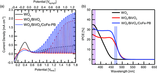
Figure 3b shows the incident photon-to-current conversion efficiency (IPCE) spectra of the three electrodes under an applied potential of 1.7 VRHE. WO3 has a high IPCE (up to 35%) in the UV region of the spectrum, whereas the IPCE is almost zero for λ > 450 nm, as expected as the bandgap is 2.7 eV. When the BiVO4 layer is added, the IPCE is extended toward the visible range, up to ≈525 nm. However, the IPCE of pristine WO3 exceeds the one of the heterojunction in the UV region (<390 nm). Upon addition of CoFe–PB catalyst, the IPCE increases both in the UV and visible region of the spectrum. As the catalyst does not modify the absorption properties of the electrode, this spectral responsivity enhancement suggests that the catalyst either boosts the separation efficiency of photogenerated carriers or suppresses their recombination at the surface, or both. However, the conversion efficiency given by IPCE is extracted only from the steady-state photocurrent: to gather information on the carrier dynamics out of equilibrium, we turn to WD-IMPS.
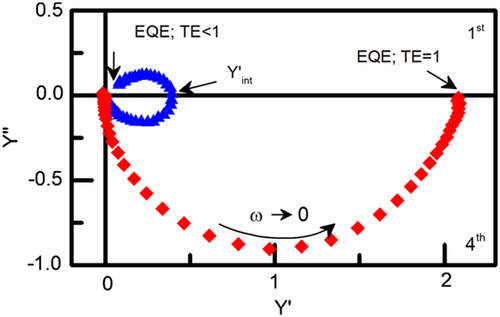
The EQE is the ratio between the number of holes transferred to the electrolyte and the number of absorbed photons. Thus, from a single IMPS measurement, it is possible to extract information on bulk transport processes and surface recombination processes of the photoelectrode.
If the positive semicircle loops back to the origin (blue plot in Figure 4), this means that surface recombination is much faster than hole scavenging; consequently, all the photogenerated charges recombine and EQE = 0. If the positive semicircle is absent (red plot in Figure 4), it means that the charge transfer is much faster than surface recombination and the EQE is governed essentially by the rate of hole transfer to the solution. In this latter case, other features might be observed: when the cell time constant is close to the charge separation time constant, two superimposed semicircles possibly merging in one distorted semicircle appear in the complex plane; if the charge separation is much faster, the spectrum results in one symmetrical semicircle.[27]
A distortion in the lower loop is observed also if full charge separation is not attained, but this can be used only to describe qualitatively the charge transfer processes at low frequencies of modulation, as the implementation of a quantitative model would need a too large number of parameters.
Figure 5 shows the IMPS spectra of the three samples under UV and blue monochromatic illumination and at different applied potentials. We used only the UV LED for WO3, which does not absorb the blue LED wavelength. For WO3/BiVO4 and WO3/BiVO4/CoFe–PB, the use of both blue and UV LEDs makes it possible to selectively excite the different layers of the photoanode, thus identifying the role of each material with respect to the heterojunction PEC activity. The intensity of the DC illumination bias used in each measurement was chosen to have the same steady-state photocurrent of 35.4 μA cm−2, thus avoiding any dependence of the involved charge carrier processes on the photocurrent density and allowing a more meaningful comparison between the different electrodes. The intensity of the AC amplitude component was 10% of the DC signal intensity. The value of the intensity of the monochromatic DC illumination bias has the same order of magnitude used in other works on similar electrodes[28] and is close to the monochromatic component of the Xe lamp used during IPCE measurements (Figure S7, Supporting Information). Figure S8, Supporting Information, compares two IMPS spectra where the DC illumination bias was given by a white LED with incident intensity of 1 sun or by the blue LED, to ensure that our discussion can be actually representative of the work conditions of the photoanode under 1 sun illumination.
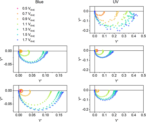
The first row of Figure 5 shows the IMPS spectra of the WO3 photoanode. Upon UV excitation, only the negative semicircle is present, meaning that surface recombination is much slower than charge transfer from the electrode to the solution.
On the other hand, the IMPS spectra of WO3/BiVO4 photoanodes show positive semicircles, indicating surface recombination up to 1.1 VRHE, that disappears at more anodic potentials for both used light sources, in agreement with another work on BiVO4.[28] The only difference between UV and blue illumination is given by the value of real-axis intercepts, which is related to the efficiency of the electrode and is commented later. Adding the CoFe–PB catalyst does not change much the shape of the spectra compared with the bare WO3/BiVO4 photoanode, but the recombination semicircle disappears at a lower applied potential (0.9 vs 1.1 VRHE), consistent with the more cathodic photocurrent onset previously discussed.
The distortion observed in the lower loop at low frequencies might be related to the surface chemistry of the photoanodes upon water photo-oxidation, as the generation of hydroxyl and peroxide moieties might introduce traps that slow down the charge transport in the photoanode.[27] The distortion is less evident in the spectra of the WO3/BiVO4/CoFe–PB photoanode and this suggests that the presence of the catalyst reduces the effect of surface poisoning.
From the IMPS data, we can now extrapolate the relative efficiency of each optoelectronic process taking place in the PEC cell.
The CSE versus applied potential is reported in the left column of Figure 6. Upon blue excitation, the CSE of WO3/BiVO4 displays a sigmoidal shape with onset about 0.9 VRHE and maximum CSE value in the high-polarization regime (1.5 VRHE) is around 17%. A similar trend is observed in WO3/BiVO4/CoFe–PB, but the CSE values display a 50% enhancement. In this model, the CSE describes only transport processes inside the bulk and is independent of the light absorption properties or surface processes, so we infer that the presence of the catalyst significantly improves the bulk electron–hole separation, especially for potential above 0.9 VRHE.
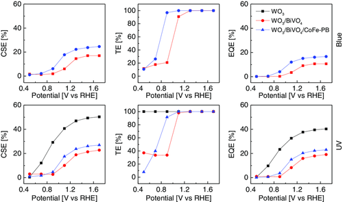
Under UV light, the WO3 photoanode shows the highest CSE, as it reaches values around 50%. Therefore, it appears that the presence of the BiVO4 layer partly reduces the collection of charges photogenerated within WO3. As with blue excitation, also under UV light, we notice a 20% enhancement of CSE upon addition of the CoFe–PB catalyst in the potential region above 0.9 VRHE.
Moving to the analysis of the TE, while pristine colloidal WO3 exhibits unitary TE in the whole used potential window upon UV illumination, the addition of the BiVO4 layer introduces superficial recombination at potentials lower than 1 VRHE, with all excitation sources. Thus, BiVO4 in the low-potential regime is less efficient than WO3 in transferring charges to the solution, meaning that the number of holes that effectively oxidize water decreases because of competing recombination. This is consistent with the shifted photoanodic onset of the WO3/BiVO4 junction with respect to bare WO3. Indeed, only when reaching a sufficiently strong anodic polarization, electrons are drawn away from BiVO4 and the electron/hole recombination process at the surface becomes negligible. On the other hand, the addition of the CoFe–PB catalyst shifts the onset of the TE to less anodic potentials, partially compensating the detrimental effect resulting from BiVO4-related recombination centers. The catalyst has therefore the beneficial effect of reducing surface recombination at low applied potentials by increasing the hole transfer rate from the electrode to the solution, as previously suggested.[3, 29]
However, the increased charge transfer rates may explain the catalyst-related shift of the photocurrent onset, but fails to elucidate the photocurrent enhancement in the high-polarization regime, where the TE is the same for all photoanodes and independent of the illumination wavelength.
The EQE versus the applied potential is shown in the right column of Figure 6. With blue LED, the catalyst slightly increases the saturation EQE from 10.6% to 16.6%, with a cathodic shift of 0.2 V. Upon UV illumination, the EQE of WO3/BiVO4 is boosted by CoFe–PB, increasing from 19% to 23%. UV-excited bare WO3 displays a higher EQE in the whole potential range with respect to the WO3/BiVO4 heterostructure irrespective of the presence of the catalyst. The IPCE measured at 1.7 VRHE is in good agreement with the EQE extracted by IMPS spectra at equivalent potential with the corresponding excitation wavelength, validating the theoretical model used to extract these efficiencies from the IMPS measurements. Compared with IPCE, IMPS allows to discern the contribution of each process to the steady-state EQE by resolving the carrier dynamics, revealing whether the EQE is limited by the charge separation in the bulk or by the charge transfer at the interface.
2.3 Efficiency Loss at the Heterojunction
The proposed data treatment highlight three critical points, namely, 1) while the EQE of the heterojunction is largely improved in the visible range, where one of pristine WO3 is negligible due to the lack of light absorption, the opposite is observed in the UV region, where EQE is lower in the heterojunction compared with pristine WO3; 2) the CSE of the heterojunction is enhanced by the deposition of CoFe–PB catalyst, and 3) the TE drop observed in the low-polarization regime in the presence of BiVO4 is partially recovered by the addition of the catalyst, while in the high-polarization regime, the TE is unitary for all samples.
The resulting Rint,het as a function of the potential in WO3/BiVO4 is shown in Figure 7 (red line), displaying a sigmoidal shape with onset at about 0.9 VRHE. In the WO3/BiVO4 electrode, as part of the electroactive WO3 surface could be directly contacted by the electrolyte, we would expect the occurrence of direct hole-scavenging pathways from WO3 to the liquid phase, but the high Rint,het of the heterojunction for potentials lower than 0.9 VRHE suggests that the large majority of holes generated inside WO3 are instead lost due to interfacial recombination with BiVO4. For higher applied potentials, Rint,het rapidly decreases, probably due to the stronger depletion field built at the WO3/BiVO4 junction facilitating the separation of the charge carriers, transport of the photogenerated holes to the valence band (VB) of BiVO4, and the injection in the electrolyte. It is however interesting to observe that even when the Rint,het plateau is reached in the high-polarization regime (1.7 VRHE), its minimum value is 53%, corresponding to the fraction of photogenerated holes recombining at the WO3/BiVO4 interface, before being effectively transferred across the heterojunction. Upon addition of CoFe–PB, Rint,het displays the same potential-dependent behavior, but the minimum value decreases to about 44% (1.7 VRHE), pointing out a positive influence of the catalyst on the charge separation process (Figure 7, blue line).
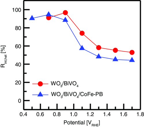
Furthermore, the addition of the catalyst has a notable impact on the CSE and TE of BiVO4, both in the UV and visible region of the solar spectrum. We observe that CoFe–PB improves the transfer of holes to the solution at low potentials, but at more anodic potentials, where the recombination of BiVO4 at the semiconductor/electrolyte interface is already negligible, the catalyst mainly affects the CSE within the BiVO4 layer. While this is counterintuitive, as catalysts are generally expected to affect mainly the TE, a similar behavior was previously observed in the work of Moss et al.[29] using more complex multiscale time-resolved spectroscopy. Consistent with our analysis, CoFe–PB was found to enhance charge collection compared with pristine BiVO4 due to catalyst-related suppression of recombination losses at the surface of the BiVO4 layer, whereas the charge TE to the electrolyte was not significantly improved. We may suggest that the main role of the catalyst in this case is to scavenge holes from the valence band of BiVO4, effectively separating them from electrons, rather than increasing the kinetics of water oxidation. The microscopic nature of the BiVO4/CoFe–PB interface is likely to play a role in in favoring the scavenging process and deserves deeper investigations.
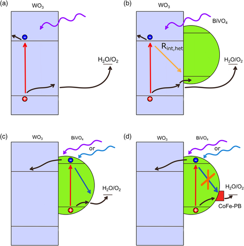
Figure 8 schematically summarizes the carrier dynamics of the studied photoanodes by shining either UV or blue light on them. Charge generation induced by photon absorption is described by red arrows, occurring in different layers, depending on the excitation wavelength, while black arrows represent charge migration processes within each semiconductor and across the heterojunction. Yellow arrows represent the recombination at the heterojunction, previously described as Rint,het, and blue arrows represent the recombination processes taking place at the BiVO4 surface, strongly reduced by the presence of CoFe–PB catalyst.
3 Conclusion
The present article establishes WD-IMPS as a powerful technique for a straightforward investigation of semiconductor photoelectrodes’ optoelectronic properties in operando PEC cells. The proposed data analysis, exploiting the information resulting from the selective excitation of different layers of heterojunctions, allows for a deep understanding of the loss mechanisms affecting the charge extraction from the semiconductors. Indeed, by isolating the contribution of the photoinduced charge carriers generated by a single semiconductor, the use of multiple-wavelength IMPS analysis shows the occurrence of the recombination process at the heterostructure interface to be identified.
By applying this approach to the WO3/BiVO4/CoFe–PB heterojunction, we identified the occurrence of interface recombination processes affecting the semiconductor junction, as well as the positive contribution of the inorganic complex catalyst on the charge separation efficiency of the BiVO4 layer. WD-IMPS therefore provides thorough and reliable information on the charge carrier dynamics in complex heterostructures, probing the operando behavior of a photoelectrode with simple, widely available facilities.
4 Experimental Section
Preparation of the Heterojunction
Chemicals and solvents were purchased from Merck, Alfa Aesar, and Carlo Erba and were used as received. Water used for material preparations was deionized through a Millipore system.
FTO/WO3 Electrodes
The preparation of spin-coated WO3 films constituted by WO3 nanoparticles was done according to previous literature.[8, 30] Briefly, the preparation of colloidal WO3 was first accomplished by precipitating a H2WO4 gel by addition of concentrated HCl to aqueous Na2WO4 (Alfa Aesar, ≥99%). After several washings of H2WO4 carried out by redispersion/centrifugation, a stable H2WO4 sol was generated by peptization with oxalic acid (Alfa Aesar ≥99.5 %) at 60 °C. The resulting colloidal suspension (having an overall mass of 8–8.5 g in the typical preparation) was densified by adding 20% w/w Carbowax (Sigma-Aldrich) and a few drops of Triton X-100 (Fluka), to improve the colloid spreadability during the subsequent FTO-coating process. Dry nanoparticulate films (colloidal photoanodes) were obtained onto the well-cleaned FTO glass (Pilkington TEC 7) by spin coating the H2WO4 aqueous colloidal precursor described earlier. In the study herein reported, six WO3 layers were sequentially deposited, each layer being thermally annealed at 550 °C for 30 min in air before the deposition of the next one. The total thickness of the electrode was 1 μm, as shown in Figure S9, Supporting Information.
FTO/WO3/BiVO4 Electrodes
Deposition of BiVO4 on WO3 photoanodes supported by FTO was achieved according to a previously published procedure,[22] inspired by an electrochemical methodology developed by Seabold et al.[31] Briefly, 10 mM Bi(NO3)3 (Sigma Aldrich ≥99%) was slowly added to an acidic solution of 10 mM VOSO4 (Alfa Aesar, 99.9%). Dropwise addition of concentrated HNO3 over a 30 min period was necessary to achieve the complete dissolution of Bi(NO3)3. After this point, the pH was rapidly increased to 4.5 using 2M CH3COONa (Alfa Aesar 99%). The resulting solution was quickly used as an electrolyte for two-electrode potentiostatic electrodeposition by applying 210 mV between FTO/WO3 and a platinum foil at room temperature for 300 s. The typical distance between the FTO/WO3 working electrode and the Pt foil was ≈3 mm. After deposition, the resulting FTO supported photoanode was abundantly rinsed with water, dried at room temperature, and finally annealed at 500 °C in air for 2 h.
FTO/WO3/BiVO4/CoFe-PB
Cobalt–iron Prussian blue catalyst (CoFe–PB)[3] was deposited by surface ionic layer adsorption and reaction (SILAR) at room temperature. Each deposition cycle was carried out as follows: first, the FTO/WO3/BiVO4 electrode was dipped in a 0.02M K3 [Fe(CN)6] (Riedel de Haen 99%) solution for 10–15 min while gently magnetically stirring the solution; this was followed by rinsing the electrode with water and immersion in 0.04M CoCl2 (Carlo Erba, 99%) for another 10–15 min under stirring. After washing out the Co(II) excess, this sequence was repeated for four times. The resulting FTO/WO3/BiVO4/CoFe–PB electrodes were then blow dried with warm air and stored in the dark at room temperature before use.
Structural and Optical Characterization
SEM images were collected on a Zeiss LEO 1430 field emission scanning electron microscope (FESEM). HRTEM and scanning transmission electron microscopy–high angle annular dark field (STEM–HAADF) characterization were performed on a FEI Tecnai F20, operating at 200 kV and equipped with EDAX Phoenix spectrometer with an ultrathin window detector for EDS.
XRD patterns were recorded using a PANalytical X'Pert Pro automated diffractometer, equipped with an X'celerator multielement solid-state detector. The diffractometer was operated in Bragg–Brentano θ/2θ para-focusing geometry using Ni-filtered Cu Kα radiation.
PEC Characterization
LSV curves, IPCE, EIS, and IMPS spectra of the photoanodes were measured in a PEC cell with a PGSTAT204 electrochemical workstation, using a three-electrode configuration with a Pt counter electrode and Ag/AgCl electrode as the reference. The electrolyte was a 0.2 m acetate solution (pH = 5). The electrodes were illuminated from the front in all the measurements in the PEC cell and the exposed area was 0.283 cm2. The LSV curves were acquired with a scan rate of 25 mV s−1, chopping the light with a frequency of 0.5 Hz.
IMPS measurements were performed in the applied bias range of 0.5–1.7 VRHE and frequency range of 0.1 Hz–10 kHz. Two monochromatic LEDs, with nominal wavelengths of 470 nm and 370 nm, were driven by an LED driver (Thorlabs DC2100) to superimpose a modulated illumination to a constant illumination bias. The sinusoidal modulation was about 10% of the illumination bias, to ensure a linear response of the LEDs. Using a beam splitter, the light was divided into two beams, one on the PEC cell to illuminate the sample and the other one on a calibrated Si photodiode (Hamamatsu) to measure the light intensity.
Acknowledgements
P.V. and A.P. contributed equally to this work. This project received funding from the European Union's Horizon 2020 research and innovation program under grant agreement no. 101006839 (CONDOR).
Open Access Funding provided by Universita degli Studi di Bologna within the CRUI-CARE Agreement.
Conflict of Interest
The authors declare no conflict of interest.
Open Research
Data Availability Statement
The data that support the findings of this study are available from the corresponding author upon reasonable request.


