Fill Factor Assessment in Hole Selective Layer Free Carbon Electrode-Based Perovskite Solar Cells with 15.5% Certified Power Conversion Efficiency
Abstract
Carbon-electrode-based perovskite solar cells (C-PSCs) are promising candidates for commercialization due to their high stability. However, the absence of a hole selective layer (HSL) often limits their performance, yielding low fill factors (FFs). Herein, a certified FF of 78.8% obtained through HSL-free C-PSCs is focused. This is found to approach the highest values reported for metal-electrode-based PSCs employing highly selective HSLs. The loss mechanisms affecting the FF in fully printed HSL-free C-PSCs are thus investigated. Methods commonly used to analyze and quantify the impact of recombination and transport losses on the FF of established photovoltage devices are assessed, and their applicability in C-PSCs is examined. In the improved devices, non-radiative recombination contributes to only 3%abs loss with respect to the FF in the radiative limit, which is attributed to an optimal diode ideality factor approaching 1.0. Moreover, contributions of shunt resistive losses are determined to be negligible. Interfacial series resistance losses at the perovskite/carbon interface are identified as the main loss channel, highlighting the importance of the quality of the contact between the perovskite and the back-contact electrode.
1 Introduction
Perovskite solar cells (PSCs) are an attractive solution-processable photovoltaic technology that offers numerous advantages in terms of ease low-cost manufacturing processes, combined with their promising light-harvesting properties. Just 12 years after the first reported 3.8% power conversion efficiency (PCE),[1] recent laboratory devices have reached efficiencies of over 25%.[2] PSCs with bandgaps of 1.6 eV, such as the most commonly employed photo-absorber material methylammonium lead triiodide (MAPbI3), can reach a theoretical maximum PCE of 31% in the radiative limit under AM1.5G conditions (Shockley–Queisser approximation).[3, 4] The theoretical model also implies a maximum current density (JSC) of 25.5 mA cm−2, a maximum (VOC) of 1.32 V,[3] and a maximum fill factor (FF) of 90%.[5] All these parameters are key indications of the quality and performance of photovoltaic solar cells. In this work, we examine the question of the FF limitations in hole selective layer (HSL) free perovskite devices.
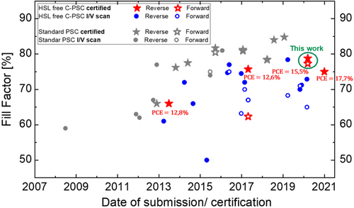
So far, recent advances have only resulted in a steep improvement of the FF in HSL-containing cells (cf. Figure 1). Therefore, literature reports have stressed the importance of the HSL to approach the radiative FF limit. Stolterfoht et al. reported an FF of 84% with an optimized Poly[bis(4-phenyl)(2,4,6-trimethylphenyl)amine (PTAA) HSL in a p-i-n configuration.[5] Wang et al. designed a poly(3,4-ethylenedioxythiophene) polystyrene sulfonate (PEDOT:PSS)/PTAA bilayer HSL interface and realized an FF of 81%.[6] The perovskite/spiro-OMeTAD interface was improved with an Al2O3/Cu:NiO interfacial layer by Wang et al., reporting an FF of 80.5%,[7] while Wu et al. reported an FF as high as 86.3% through oleylamine surface functionalization of this interface.[8]
For commercial applications, however, such organic HSLs are problematic due to high price and low material stability.[9] In contrast, printed HSL-free carbon-electrode-based perovskite solar cells (C-PSCs) have proved to be most promising in terms of up-scalability and long-term device lifetimes as all electrode layers are chemically very stable and enable resistance against reverse bias-related degradations.[10-13]
Here, high-temperature C-PSCs are being investigated. These devices are not compatible with organic conventional HSLs, considering the high-temperature processes of over 400 °C necessary for their treatment. Several studies have investigated the incorporation of thermally stable inorganic nickel oxide (NiO) as HSL. However, no significant improvement in device performance has been shown, which we attribute to the specific mesoscopic structure of the high-temperature C-PSCs, in which the HSL layer would have to be deposited before the perovskite absorber is imbedded.[14]
In this work, we report a “certified” stabilized efficiency of 15.5% and an FF of 78.8% (“certified” reverse scan) for HSL-free n-i-p perovskite cells with a graphite back electrode, a value which remains to the best of our knowledge the highest reported “certified” FF for HSL-free C-PSCs, albeit the existence of a higher reported “certified” efficiency (cf. Figure 1).[15] We also recognize here an FF of 78.6% (“non-certified” reverse scan) reported for the same photo-absorber.[16] We explore the physical loss mechanisms limiting the FF by theoretical considerations and measurements of certified current–voltage characteristics, as well as JSC–VOC, impedance spectroscopy, and VOC decay characterization. This astonishingly high value of almost 79% gives the impression that transport and recombination losses do not have much influence on the FF, but the efficiency would still be limited by recombination losses considering the rather low VOC value obtained of 0.9 V. To find out the reason behind this behavior, we present a detailed loss analysis based on electrochemical impedance spectroscopy (EIS) and JSC–VOC measurements. The diode ideality factor of 1.00 is almost ideal to obtain a high FF. Resistivity loss due to shunts is negligible. Although no metal back contact is used, the contact electrode series resistance losses are low, but not optimal, and amount to ≈12.6 Ω, equivalent to1.19 Ω cm2.
The novelty of our work, based on certified measurements of this considerably high FF albeit the absence of an HSL, aims, therefore, to assess the loss mechanisms affecting the FF in high-temperature monolithic carbon-based perovskite solar cells while applying and comparing methods commonly employed to analyze the FF performance of established silicon photovoltaic devices. To the best of our knowledge, this sort of analysis is being reported for the first time for carbon electrode HSL-free devices.
2 Results and Discussion
2.1 Solar Cell Architecture and Certified I/V Characteristics
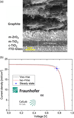
The C-PSC in question for this study is based on a commercial HSL-free monolithic device architecture (Solaronix) that was later filled with a perovskite precursor. The electrodes are screen-printed on a fluorine-doped tin oxide (FTO) glass substrate and consist of a compact titanium oxide (TiO2) hole blocking layer, a mesoporous TiO2 electron transport layer, a mesoporous zirconium oxide (ZrO2) space layer, and a high temperature processed carbon electrode. The scanning electron microscopy (SEM) image of the cross section of the ternary cation perovskite filled cell is presented in Figure 2a.
We filled this triple mesoscopic C-PSC stack by drop casting a precursor of triple cation perovskite Rb0.05Cs0.1FA0.85PbI3. The filling method involved a delayed crystallization process in a closed solvent vapor environment. Therefore, the samples were immediately covered after drop casting the precursor solution to ensure an optimal infiltration.[15, 16] For our investigation, commercially available (Solaronix) MAPbI3-based devices with the same electrode structure were taken as a reference. This ensured that the sole difference between the reference and the triple cation filled cells was the perovskite absorber itself. A detailed description of the fabrication protocol is provided in the Experimental Section. Energy-dispersive X-ray spectroscopy images showed that the filling of both perovskite absorbers is homogeneously distributed (cf. Figure S1, Supporting information). Hence, we can exclude that the observed lower performance of the reference samples is due to technological shortcomings such as incomplete filling. This highlights that the improved performance of the triple cation device is, in fact, due to improved crystal quality and interfacial coupling as demonstrated later. Tauc plots based on the absorbance spectra from ultraviolet–visible spectroscopy measurements of both investigated perovskite compounds revealed an optical energy bandgap of 1.49 and 1.55 eV for the Rb0.05Cs0.1FA0.85PbI3 and MAPbI3 photo-absorbers, respectively, whereas the first is closer to the Shockley–Queisser efficiency limit (cf. S2 in the Supporting Information).
The efficiency of the best-performing triple cation absorber Rb0.05Cs0.1FA0.85PbI3 device was certified at the Fraunhofer ISE Calibration Laboratory, yielding a certified stabilized efficiency of 15.5% with a steady-state maximum power point (MPP) voltage VMPP and current density JMPP of 756 mV and 20.4 mA cm−12, respectively (cf. Figure 2b). In addition to steady-state values, a certified current–voltage scan with low hysteresis was performed, yielding a JSC of 22.4 mA cm−2 and VOC of 881 mV in the reverse scan. The measurement was performed using a class AAA steady-state solar simulator, where the irradiance and temperature were controlled and monitored throughout the calibration. First, the I/V curve was determined from both scan directions. Then, the certified efficiency measurements were conducted through tracking of the current at a fixed voltage at the MPP, whereby the stabilized PCE refers to the average value over 300 s. Refer to the Supporting Information for the full calibration report.
The obtained stabilized efficiency of 15.5% is, to the best of our knowledge, the highest “certified” steady-state efficiency reported for HSL-free carbon-based perovskite devices. However, we recognize here that higher efficiencies have been reported in the literature for “non-certified” C-PSCs.[15, 17-22] While the present work was in peer review, a highly significant study has been published, reporting on “certified” efficiency obtained through the I/V curve reaching 17.7% and an FF of 75%.[23]
The PCE was not the only parameter that was found to reach record numbers for HSL-free C-PSCs, as the FF obtained from the certified measurements reached 78.8% in the reverse scan and 77.1% in the forward scan, with a very low hysteresis index of 2%. Another way to assess the FF from the calibration report is to refer to the certified steady-state MPP parameters, JSC and VOC, obtained from the reverse and forward scans, yielding a “steady-state FF” of 78.1% and 77.7%, respectively, with a calculated hysteresis index of 0.5%. As can be seen in Figure 1, especially when excluding published values showing a high hysteresis index, this certified FF represents the highest reported value for HSL-free C-PSCs. Moreover, the obtained FF approaches the record values for PSC devices with metal electrodes and highly selective HSLs. This is a remarkable result as it is scrutinizing the current conception that a separate HSL is crucial to obtain the highest experimental FF values. In the following, we will, therefore, discuss the theoretical physical constraints on the FF, examine its full potential, and introduce methods to quantify the FF-related loss mechanism.
2.2 Theoretical Analysis of Obtained FF Values
2.2.1 Diode Model and Relation to Recombination Loss Mechanisms Limiting the FF
The shunt and series resistances have an influence on the MPP, consequently having an impact on the FF. Lower RSH values lead to loss of power due to parasitic current pathways in parallel to the ideal diode, whilst higher RS values shift the working point essentially due to a parasitic voltage drop over the series resistance, which is reflected in a decreasing slope of the current–voltage curve near the VOC point.
In HSL-free C-PSCs, the series resistance losses can occur due to the “lateral” ohmic resistivity of the front transparent conductive oxide (TCO) electrode and carbon back-contact electrode, as well as due to the “vertical” transport losses in bulk materials and at interfaces between the layers constituting the cell, particularly between the TiO2 charge transport layer and the FTO front contact, the TiO2 and the perovskite, as well as the graphite and the perovskite.
The diode ideality factor indicates the dominant type of recombination mechanisms in the device depending on its value, typically bounded between 1 and 2, which is conditioned by the charge carrier density and the reaction order γ of the dominant form of recombination.[25] Electron–hole recombination occurs directly in the form of pure radiative recombination or additional non-radiative recombination, ideally leading to an ideality factor of nID = 1; in a device with high defect state recombination, the ideality factor would be closer to 2.[16]
According to a simulation-based study carried out by our group and others, at VOC, the dominant internal recombination loss mechanism in C-PSCs happens at the perovskite–graphite electrode interface with the perovskite/TiO2 interface representing the second largest recombination loss channel.[26]
2.2.2 The Fill Factor and The Current–Voltage Curve
The current–voltage FF cannot be deduced analytically from the Shockley diode equation. Several studies have been conducted to determine an analytical approximation of the current–voltage measurements of solar cells based on experimental VOC and JSC values, from which the FF can eventually be extracted.[27-30] However, an accurate measure of the FF remains to be dependent on experimental and actual measurement conditions in which all sources of losses are taken into account.
The MPP denotes the point at which the cell reaches its maximum power output. Practically, however, especially in the context of measurements dealing with perovskite solar cells, the determination of the MPP can prove to be difficult due to transient (e.g., hysteretic) behavior. In this work, we discuss for the first time an FF value obtained from a certified stabilized measurement.
2.2.3 Accounting for Resistivity Losses: pFF and FF0
In silicon-based photovoltaic solar cells (Si-PV), there are two main established methods to assess the contributions of resistivity losses to the FF: through analyzing the so-called pseudo fill factor, pFF, and ideal fill factor, FF0. As we show in the following, the approaches can also be directly applied to perovskites if transient effects in the measurement are excluded, e.g., by stabilized characterization.
Both methods rely on JSC–VOC measurements.[31-33] It is worth mentioning here that due to transient effects, JSC–VOC for the perovskite devices was performed through the original method consisting of steady-state measurements, rather than by the flash-lamp-based Suns-VOC method introduced by Sinton et al., which is most common for Si-PV.[33, 34] The pFF is determined based on JSC–VOC pairs obtained at different illumination densities, whereas FF0 is assessed from the diode ideality factor obtained from JSC–VOC measurements and the VOC measured at AM1.5 g. In an ideal solar cell, the difference between pFF and FF0 should be marginal, but it is important to note that the analytical method to estimate FF0 is only viable for devices showing low recombination losses.[35]
Both pFF and FF0 represent fill factor values for which resistivity loss contributions have been eliminated, in which FF0 represents the fill factor values purely influenced by recombination losses, while pFF also includes the influence of shunt resistance (RSH) losses. Thus, the difference between pFF and FF0 can be considered to estimate the impact of the recombination losses on the overall FF of the device.
In a Shockley diode model, as long as the device does not suffer from severe resistive losses, the effects of RS and RSH are negligible at open and short circuits.
It is to be noted that FF0 is only dependent on the VOC and nID of the device, which are in turn affected essentially by non-radiative recombination losses. For a bandgap of 1.6 eV, the theoretical VOC of 1.3 V results in a theoretical FF limit of 90%.
Both expressions assume a linear drop of the voltage along the device cross section, although that is not entirely accurate as the voltage value fluctuates due to the nonuniformity of the charge carriers throughout the device.[38] Thus, we find it necessary to mention another approach used in Si-PV to estimate the FF without taking account of the outer voltage value obtained through the I/V measurements. This consists of the implied fill factor, iFF, which can be determined through calculating the FF value either through Green's equation or through Swanson and Sinton's equation, by replacing the voltage value with the implied open-circuit voltage value, iVOC, which in turn depends on the carrier concentration.[38-40]
2.3 Effect of Non-Radiative and Resistivity Losses
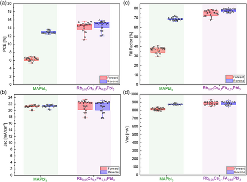
To shine a light on the high FF obtained through our HSL-free C-PSCs, a range of devices filled with the triple cation absorber Rb0.05Cs0.1FA0.85PbI3 and the MAPbI3 as references were manufactured. Figure 3 shows the I/V performance of the devices in the reverse and forward scan directions, demonstrating that overall, the triple cation C-PSC cells display a higher FF and a considerably lower hysteresis as compared to the reference. Considering the average values, the MAPbI3 shows a 42% FF-hysteresis index, in comparison with 4% for the triple cation devices for which the best device possesses a 2% hysteresis index. The hysteresis is only marginally affecting the VOC and JSC, which means that the low PCE can be attributed to the pronounced I/V hysteresis affecting drastically the FF of the MAPbI3 cells. It is to be noted that the MAPbI3 reference devices show a more reproducible pattern, and that can be attributed to the fact that the samples are done following an automated commercial-oriented manufacturing process. (More details can be found in the Experimental Section.)
To distinguish the impact of resistivity losses on the FF of our devices, we measured the VOC decay to assess the effect of the shunt resistance on the cells and employed EIS to quantify and determine the influence of the series resistance on the performance of the devices.
For open-circuit voltage decay, the VOC is first stabilized under illumination. This is necessary to ensure that there is no transient effect related to ion movement and that slow traps are filled. Then, the decay of the VOC is measured as the light is rapidly switched off. Under steady-state illumination, the VOC depends on the quasi-Fermi-level splitting, which in turn is logarithmically proportional to the charge carrier density determined by a balance of photo-generation and recombination processes. When the light is switched off, this balance is disturbed, as there are no new photo-generated charge carriers. One typically observes a rapid decay of the voltage due to the fast extinction of the largest proportion of charge carriers in radiative and fast non-radiative decay processes due to carrier recombination or shunts. After this fast decay, long-living charge carriers contribute to a much slower decay of the remaining VOC levels.
Figure 4a shows the VOC decay measurements of the studied devices. The purple trend line represents the VOC decay of the Rb0.05Cs0.1FA0.85PbI3 cell, and the green line represents the voltage decay of the MAPbI3 reference device. From the measurements, some transient decays were observed with the triple cation device showing a slower decay (cf. Figure 4 and refer to the discussion in S4 in the Supporting Information). The lighter-colored trend lines for each variation correspond to the VOC decay of the same device connected in parallel to an external 1 kΩ shunt resistor. The sharp decrease in VOC decay reaching 0 V in a matter of microseconds for the MAPbI3 can be attributed to the fast-recombining charge carriers at the graphite electrode due to the external current in the introduced ohmic shunt resistance. This indicates that the MAPbI3 device manifests an internal shunt resistance much greater than 1 kΩ. At this point, it is important to consider that both devices comprise the same porous layer stack and differ only in the filled perovskite absorber. We expect shunts to occur mainly due to defects in this porous stack, providing electrode contact between the carbon and the FTO electrode. Hence, we can conclude that both devices display low shunt resistance losses with an RSH >> 1 kΩ (cf. S5 in the Supporting Information for an estimated RSH value), in other words, the performance of the devices is not limited by shunt resistance losses. Notably, even after introducing the external shunt resistor, the triple cation device shows an open-circuit voltage of ≈200 mV after 45 ms under dark, which requires further investigation, but indicates the presence of high charge carrier densities in deep traps with long lifetimes. Time-resolved photoluminescence (TRPL) spectroscopy measurements on perovskite-filled mesoporous TiO2 supported this assumption revealing a longer carrier lifetime for the Rb0.05Cs0.1FA0.85PbI3 perovskite compared to the reference MAPbI3 sample (cf. Figure 4b). A bi-exponential fit of the photoluminescence (PL) decay yielded carrier lifetimes of τ1 = 49 ns and τ2 = 437 ns for the triple cation perovskite compared to τ1 = 19 ns and τ2 = 168 ns for the reference MAPI perovskite sample. The slower decay obtained for the triple cation sample suggests lower charge carrier recombination losses.
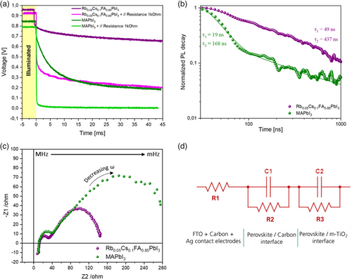
Additionally, transient PL quenching measurements were performed on full devices. The technique consists of toggling between open-circuit and short-circuit conditions under constant illumination. The recorded measurements suggested a fast charge transport for the triple cation perovskite absorber in which the VOC of the device shows an almost perfect box-shaped behavior after a rapid switch from short-circuit to open-circuit conditions (cf. S6 in the Supporting Information).[14, 16]
Series resistance losses were evaluated through EIS measurements. We employed the equivalent circuit model to fit the Nyquist plots of MAPbI3 and Rb0.05Cs0.1FA0.85PbI3 cells (cf. Figure 4c,d), which shows that the ohmic series resistances R1 induced by the cell electrodes is similar in both devices at 12.6 and 12.3 Ω, respectively. This is not surprising as it represents the “outer” series resistance losses of the bulk TCO and the bulk graphite layer, which we do not expect to differ as the layer stack of both devices is identical. We find it necessary to note here that the EIS measurements were performed without a shadow mask at 1 sun intensity over a total active area of 1.44 cm2. For large-scale devices, this value would be considered detrimental, but it does not affect the FF values reported in this work as they correspond to measurements performed over a small masked area of 0.09 cm2. In the Nyquist plots, we attribute the (left) semi-circle in the high-frequency region to the perovskite carbon interface (R2 and C1). The (right) semi-circle in the low-frequency region corresponds to the I/V behavior of the diode considering its light dependency and can be attributed to the charge transfer at the perovskite/m-TiO2 interface (R3 and C2).[41, 42] In a previous study by our group and others, Bogachuk et al. compared carbon-based electrodes produced from different graphite flake types and demonstrated that the FF in mesoporous C-PSCs is influenced by both the sheet resistivity of the graphite-based electrode (R1) and the interfacial resistance at the perovskite carbon contact (R2).[43] As the cell geometry and sheet resistivity of electrodes were the same in both cell types (and is not altered by the absorber), the EIS measurements highlight that the interfacial resistance at the perovskite carbon contact is lower in Rb0.05Cs0.1FA0.85PbI3 cells than in MAPbI3 cells, amounting to 18.5. and 31.5 Ω, respectively. The higher interfacial resistance along with the lower FF obtained for the MAPbI3 samples suggests that the perovskite carbon interface in fact contributes to the FF losses. Moreover, it is evident from the Nyquist plots the huge improvement at the perovskite/m-TiO2 interface for the triple cation absorber, which can be attributed to an optimized crystallization through the delayed saturated solvent vapor environment. The impedance spectroscopy measurements reported here were conducted at an applied bias voltage of 0.6 V, and results for different applied voltages ranging from 0.4 to 0.8 V did not vary substantially (cf. S7 in the Supporting Information). The perovskite/carbon interfacial capacitance C1 was measured at 0.25 and 0.48 μF for the MAPbI3 and Rb0.05Cs0.1FA0.85PbI3 cells at a frequency of 1.9 × 10³ and 1.7 × 10⁴ Hz, respectively. The relatively higher capacitance for the triple cation device, in combination with the higher FF, may be attributed to a beneficial interface formation, and thus charge transport between the perovskite and charge extraction layers as compared to the reference devices. This optimized interface formation at the level of the triple cation photo-absorber and the adjacent interfaces can be due to an improved crystallization inside the mesoscopic electrode stack. This improved crystallization is also reflected in reduced interfacial resistance losses.
From the obtained VTFL for Rb0.05FA0.85Cs0.1PbI3 and MAPbI3 perovskites, the trap densities were determined to be 3.66×1017 cm−3 and 9.28×1017 cm−3, respectively, which suggest higher non-radiative recombination in MAPbI3 perovskite compared to the triple cation. This was further investigated later. Furthermore, from Equation (6), the obtained charge mobilities account for 4.6× 10⁻⁴ cm2 V−1 s−1 for Rb0.05FA0.85Cs0.1PbI3 and 1.4×10⁻⁴ cm2 V−1 s−1 for MAPbI3 perovskites. This clearly demonstrates enhanced charge carrier transport properties of C-PSCs with mixed cation perovskite, which corroborates the excellent FF of such cells demonstrated earlier.
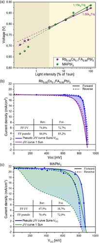
The stronger decrease of VOC at low light intensities below 0.01 sun for the MAPbI3 sample indicated lower shunt resistance losses. In contrast, for the Rb0.05Cs0.1FA0.85PbI3, there is no collapse of the VOC for light intensities as low as 0.003 mW cm−2 (cf. Figure 5a).
Pseudo I/V curves from JSC–VOC measurements plotted against device I/V curves measured at 1 sun intensity, as presented in Figure 5(b,c), show the difference between the FF obtained from the current–voltage curve measured at 1 sun illumination and pFF of a triple cation-based device. Note that the device presented in the figure does not represent the certified record device. The shaded areas, purple for the triple cation cell and green for the reference cell, represent the resistivity losses due to transport limitations and the ohmic resistance.
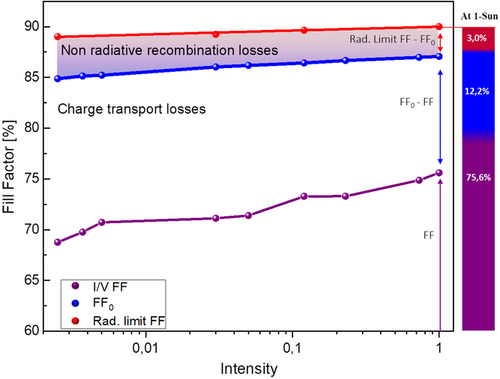
From the difference between pFF and the current–voltage FF (cf. Figure 6), the contribution of resistivity losses to the FF can be assessed to 11.2%abs in the reverse scan and 12.5%abs in the forward scan. The calculated ideal FF0 for the triple cation device is 87.0%, showing a marginal difference compared to the experimental pFF of 86.0% obtained through the pseudo current–voltage curve. The iFF value was calculated for this absorber and was found to be ≈86.3% (cf. S9 in the Supporting Information). Thus, for our triple cation perovskite devices, considering that the pFF and FF0 align well, we conclude that both Green's and Swanson and Sinton's equations provide a good estimation of the ideal FF.
For the reference MAPbI3-based device, the significant deviation between the FF0 reaching a value of 85.7% and the pFF measured at 76.4% suggests that the device is manifesting high transport losses. It is also important to note that the approach to calculate the ideal FF0 and the estimation of resistivity losses through evaluating the difference between the current–voltage FF and the maximum achievable FF will lead to overestimated values for devices showing high recombination losses.[35]
Finally, the assessment also reveals insights into the low-light FF performance of the triple cation device, as shown in Figure 6. The plot displays the FF measured from the reverse current–voltage scans (purple points) and relates these to the FF without taking the resistive losses into account (FF0, blue) as well as to the theoretical maximum FF at the corresponding illumination intensity (red). The difference between the purple and blue data points represents the FF losses due to charge transport limitations, showing an increase in the charge transport losses at low light intensities, i.e., low generation rates. At 1 sun, the transport losses amount to 12.5%abs with respect to the theoretical maximum. Finally, relating the blue to the red data points implies that the remaining non-radiative recombination losses have a small influence on the FF, accounting for 3% at 1 sun.
The performance of PSCs at lower light intensities reflects the effect of the shunt resistance on the device. Our triple cation device displays an FF of 68% at the lowest light intensity measured compared to 34% for the MAPbI3 reference at the same intensity (less than 1 mW cm−2) (cf. S10 in the Supporting Information for the reverse current–voltage scans of both devices at different light intensities). The better performance of the Rb0.05Cs0.1FA0.85PbI3 device even at lower light intensities implies a high shunt resistance, thus suggesting that the FF of our C-PSCs is not affected by shunt resistance losses. Therefore, based on our assessment of the influence of non-radiative recombination and transport losses on the FF, we find that with the optimized filling process and the optimized perovskite composition of the triple cation perovskite, recombination losses to the FF have been minimized.
3 Conclusion
In this work, a “certified” steady-state PCE of 15.5% obtained for an HSL-free C-PSCs filled with a triple cation perovskite absorber was reported, in which the infiltration of the perovskite absorber in the mesoporous layers involved a delayed saturated solvent vapor crystallization. This study analyzes the fundamentals behind the high obtained “certified” FF of 78.8%, which is among the highest reported in the literature and most notably, the highest FF for HSL-free PSC. We investigated the effect of non-radiative recombination and transport losses on the FF of our devices. JSC–VOC measurements were carried out, from which pseudo current–voltage characteristics were derived. We compared two devices of the same structure with two different perovskite absorbers: an MAPbI3-based device serving as a reference and a high-efficient triple cation Rb0.05Cs0.1FA0.85PbI3-based perovskite. The pseudo FF from JSC–VOC measurements, which allows assessing the highest achievable FF of a device without the influence of transport losses, was found to reach 87.0% for the triple cation device, showing a good agreement to the calculated so-called ideal FF0. Our measurements confirmed that the influence of the non-radiative recombination losses on the FF was marginal (only 3%abs). Moreover, TRPL measurements at 1 sun revealed a longer carrier lifetime for the triple cation photo-absorber compared to the MAPbI3 reference. Space-charge-limited current measurements confirmed that bulk mobility was three times higher with the triple cation perovskite.
Additionally, by comparing EIS measurement of devices containing the two different photo-absorbers, we demonstrate that the dominant transport losses mainly occur at the interfaces between the perovskite and the charge extraction layers. By the incorporation of the Rb0.05Cs0.1FA0.85PbI3 perovskite and the implementation of the delayed solvent vapor crystallization process, the interfacial resistance could be significantly improved compared to the MAPbI3 device.
So far, in the literature on perovskite solar cells, it was believed that high FF values could only be achieved with highly selective electrode layers. However, the high FF of the here discussed HSL-free, carbon-electrode-based devices demonstrated that this perception needs to be revised as the effect of recombination losses on the FF is much less detrimental as compared to transport losses, which have been successfully overcome in this study. To the best of our knowledge, a systematic study which compares the different analytical methods to quantify the loss mechanisms influencing the fill factor employing pFF, FF0, and implied FF is being reported for the first time for carbon electrode-based PSCs. The study demonstrates the feasibility of reaching the highest FFs with HSL-free PSC without the need for expensive and potentially unstable HSLs. These findings are thus encouraging that further improvement of both the perovskite composition, precursor formulation, and controlled crystallization process may lead to an even further enhancement of the FF.
4 Experimental Section
Materials
Rubidium iodide (RbI), cesium iodide (CsI), dimethyl sulfoxide (DMSO), dimethylformamide (DMF), and formamide were purchased from Sigma-Aldrich. Formamidinium iodide (FAI) was purchased from Greatcell Solar Materials. Lead iodide (PbI2) was purchased from TCI Chemicals. The chemicals were used as purchased.
Perovskite Precursor Solution
The absorber Rb0.05Cs0.1FA0.85PbI3 was prepared in a nitrogen-filled glovebox; 0.0127 g of RbI, 0.0311 g of CsI, 0.1754 g of FAI, and 0.5808 g of PbI2 were weighted and sequentially dissolved in 50 μL formamide, 200 μL DMSO, and 750 μL DMF. The solution was stirred at room temperature at 1400 rpm for 2 h.
Monolithic Electrodes and Reference Devices from Solaronix
Commercial Solaronix monolithic HTL-free electrodes were built on an FTO-coated glass substrate. The 25 × 20 mm2 substrates were pre-scribed and pre-lasered, and consisted of a compact titanium oxide (TiO2) hole blocking layer fabricated from spray coating titanium diisopropoxide bis(acetylacetonate) diluted in a solution of 99% ethanol at a 1:80 volume ratio, followed by a screen printed mesoporous TiO2 layer of 0.6 μm thickness to facilitate electron transport, a 1 μm thick mesoporous zirconium oxide (ZrO2) space layer, and a high temperature processed carbon-graphite layer as back-contact electrode with an overall active area of 12 × 12.5 mm2. The monolithic electrodes were sintered at 400 °C for 30 min as per manufacturer's recommendation prior to use. The (5-AVA)-MAPbI3 filled reference devices were prepared by Solaronix through ink-jet printing.
Filling Protocol
The filling was done in the air under a fume hood. The pre-sintered monolithic electrode, glass petri dishes, and the perovskite precursor solution were preheated at 50 °C, and then heated up gradually to 70 °C at a ramp time of 3 min. Once the hot plate reached 70 °C, 6 μL of perovskite precursor solution was drop-casted onto preheated substrates and rapidly covered with a petri dish and left to anneal for 2 h.
Characterization
The SEM image in Figure 2a was captured through a Zeiss Auriga 60 electron microscope.
Ultraviolet–visible spectroscopy measurements were performed through a PerkinElmer Lambda 1050. The absorbance data was obtained from the measured transmittance and reflectance measurements at a wavelength range of 400–900 nm.
Current–voltage measurements in Figure 3 were conducted through a class A Xenon arc lamp light source under constant AM1.5G illumination. The simulator was connected to a Keithley 2400 source meter. The cell was masked with an aperture of 0.096 cm2. Steady-state VOC was tracked for 200 s first, and then the reverse scan was measured first from 1.1 to −0.1 V followed by the forward scan from −0.1 to 1.1 V at a scan rate of 50 mV s−1.
Suns-VOC measurements in Figure 5 and 6 were operated through the same solar simulator using light filters to simulate the different light intensities. The light intensity was checked for each change of filters using a calibrated silicon reference device.
VOC decay measurements reported in Figure 4a were recorded for 45 ms, 90 ms, and 2 s (cf. S4 in the Supporting Information). A red LED light from Thorslabs of wavelength 635 nm was used to illuminate the cells. The devices were measured in a dark room and kept under constant illumination for light soaking before switching off the light to track VOC decay. PicoScope 5000 series was used to acquire the measurements.
The SCLC measurement was carried out using an Ivium CompactStat by performing a current–voltage sweep from 0 to 4 V with a scan rate of 10 mV s−1. The extended data points (>4 V) were obtained by applying a constant voltage with a step size of 200 mV using an external power supply and measuring the resulting current.
PL decay measurements in Figure 4b were performed with a homemade setup that allows to track the luminescence decay from the steady state, i.e., from illuminated state over a time period much longer than conventionally used ps-laser illumination. The sample was illuminated with a CW laser (Coherent OBIS, wavelength 660 nm, 100 mW, laser spot widened to ≈1 cm2) that was modulated via a function generator (Hamamatsu). The PL signal was detected with a photodiode on which an optical filter was mounted. The signal was recorded via an amplifier on a fast digital oscilloscope (PicoScope 5000).
EIS measurements in Figure 4c were measured at a frequency range of 1 MHz to 100 mHz at negative applied bias voltage using an Ivium CompactStat device under 100kLUX illumination.
Acknowledgements
The authors acknowledge funding by the project UNIQUE, supported under SOLARERA.NET and cofunded by ANR, PtJ, MIUR, MINECOAEI, and SWEA. SOLAR-ERA.NET was supported by the European Commission within the EU Framework Programme for Research and Innovation HORIZON 2020 (Cofund ERA-NET Action, no. 691664). This work was supported by funding from the European Union's Horizon 2020 research and innovation program under Grant Agreement No. 763989 (APOLO). This publication reflects only the author's views, and the European Union is not liable for any use that may be made of the information contained therein. The authors acknowledge funding by the Project PROPER financed from the German Federal Ministry of Education and Research under the funding No. 01DR19007. S.Z. gratefully acknowledges the Ph.D. scholarship support of the DAAD. D.B. acknowledges the scholarship support by the German Federal Environmental Foundation (DBU). The authors thank Jutta Zielonka for the scanning electron microscope images.
Open access funding enabled and organized by Projekt DEAL.
Conflict of Interest
The authors declare no conflict of interest.
Open Research
Data Availability Statement
The data that support the findings of this study are available from the corresponding authors upon reasonable request.


