Phase Transitions in a Perovskite Thin Film Studied by Environmental In Situ Heating Nano-Beam Electron Diffraction
Abstract
The rich phase diagram of bulk Pr1−xCaxMnO3 resulting in a high tunability of physical properties gives rise to various studies related to fundamental research as well as prospective applications of the material. Importantly, as a consequence of strong correlation effects, electronic and lattice degrees of freedom are vigorously coupled. Hence, it is debatable whether such bulk phase diagrams can be transferred to inherently strained epitaxial thin films. In this paper, the structural orthorhombic to pseudo-cubic transition for x = 0.1 is studied in ion-beam sputtered thin films and differences to the respective bulk system are pointed out by employing in situ heating nano-beam electron diffraction to follow the temperature dependence of lattice constants. In addition, it is demonstrated that controlling the environment during heating, that is, preventing oxygen loss, is crucial in order to avoid irreversible structural changes, which is expected to be a general problem of compounds containing volatile elements under non-equilibrium conditions.
1 Introduction
Current and future technologies increasingly exploit the unique characteristics of metal oxide thin films,[1-3] where a plethora of physical properties can be tailored by temperature and composition dependent phase transitions. By definition, these compounds contain volatile components, that is, elements in gaseous state at processing or even operating conditions. Prominent examples are TiOx for improved solar cell contacts,[4, 5] ZnO for ultraviolet light emitting diodes,[6, 7] La1−xSrxMnO3 for solid oxide fuel cells,[8, 9] MgO for magnetic tunneling junctions,[10-12] Li1−xCoO2 for solid state batteries,[13-15] or Pr1−xCaxMnO3 (PCMO) for neuromorphic computing.[16-18] As a general feature, the oxygen activity adjusted by ambient conditions delicately controls properties and reaction paths in such systems. Referring to the metal oxides related to solid state batteries and neuromorphic computing, such reaction paths and also applications rely on controllable, reversible phase transitions. Hence, typical non-equilibrium operation and processing conditions offer the route to steer the latter,[19-21] but also involve the risk of undesired reaction paths. In addition, the incorporation in structured devices raises the question whether and how phase diagrams obtained on bulk materials can be transferred to the nanomaterial counterparts.
Calcium doped PrMnO3 (Pr1−xCaxMnO3, PCMO) is a prominent representative of strongly correlated manganites discussed in the context of neuromorphic computing, but also related to third generation photvoltaics[22-24] and catalysis.[25-28] Due to strong correlations, the system – as many other strongly correlated materials[29] – has a rich phase diagram with several ordered phases showing remarkable properties.[30-32] Various studies have focused on magnetic ordering at low temperature which is well understood.[33-35] In addition, phase transitions at higher temperature of several hundred degrees Celsius have been revealed by neutron and X-ray diffraction experiments on PCMO powders for low Ca concentrations.[33, 36] They show the transition from an orthorhombic to pseudo-cubic phase with small but still finite deviations of the lattice parameters from an ideal cubic structure. These changes are related to a reduction of the cooperative Jahn-Teller (JT) distortion as well as the alternating tilt of neighbouring MnO6 octahedra in the high-temperature phase. Still, there is no direct evidence of orbital ordering driving the phase transition and latest results suggest that the orbital ordering above room temperature is induced by octahedral tilting.[37]
A major unsolved problem, however, is whether and how such data can be transferred to epitaxial thin films, which are the typical basis for technological application. More generally, this is equivalent to the question whether bulk phase diagrams remain unchanged in thin film systems. In fact, particularly in the context of transition metal oxides, various reports exist about tunable physical properties by epitaxial strain and oxygen vacancies possibly affecting phase transition temperatures as well.[38-41]
In this work, we investigate phase transitions at high temperature in PCMO (x = 0.1) grown as a 400 nm thick epitaxial film on a SrTiO3 (STO) substrate. In order to extract temperature-dependent lattice parameters we use nano-beam electron diffraction (NBED) in a 4D scanning transmission electron microscopy (4D-STEM) mode.[42] Hence, individual domains of the typically nanotwinned films can be addressed in contrast to macroscopic X-ray or neutron diffraction studies. Furthermore, during the in situ heating experiments, the environmental capabilities of the electron microscope are used to compare reaction paths in ultra-high vacuum (UHV) and 10 Pa oxygen partial pressure ambient conditions. In the latter case, a reversible orthorhombic to pseudo-cubic phase transition is observed, while in the former case, an irreversible phase transition associated with the appearance of superstructure reflections occurs, which completely suppresses the orthorhombic to pseudo-cubic phase transition. These results will be discussed in terms of oxygen vacancies whose formation is controlled by the ambient conditions.
2 Results and Discussion
Prior to considering the temperature dependence of the given lattice parameters, a brief overview of the crystal structure of PCMO as well as the thin film epitaxy and heterogeneity shall be given. Figure 1a illustrates the expected tilt pattern of corner-sharing MnO6 octahedra in PCMO (a−a−c+ in Glazer notation[43]) leading to an orthorhombic Pbnm unit cell. For the sake of simplicity, A-site atoms, that is, Pr and Ca are not shown. Compared with the cubic unit cell of an ideal perovskite like STO containing only one octahedron which is neither tilted nor distorted, the lattice vector PCMO[001] is approx. two times larger due to the tilt alternation. Similarly, PCMO[100] and PCMO[010] are approx. times larger and rotated by approx. 45°. Consequently, six epitaxial growth relations of PCMO on a cubic STO substrate (with STO(001) surface termination) exist as illustrated in Figure 1b. The moduli of the corresponding bulk lattice vectors at room temperature are given in Table 1. Importantly, a change of the space group of PCMO is not expected in the pseudo-cubic phase, in which the octahedral tilt is strongly reduced but still finite.[33, 36]
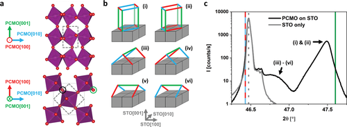
The Θ − 2Θ X-ray diffraction (XRD) scan of the epitaxial thin film presented in Figure 1c shows a clear peak close to the PCMO(004) bulk value (solid green line) and only subtle differences compared with the reference scan of a pristine substrate in the range of the PCMO(220) bulk value (dashed red-cyan line). Thus, the XRD data suggests predominant growth relations (i) and (ii) and the position of the corresponding peak yields +0.2 % tensile strain of the out-of-plane PCMO[001] lattice parameter being consistent with previous reports about significant deviations from bulk properties in relatively thick PCMO films due to both misfit as well as preparation related strain that is induced by point defects and variations in octahedral tilt.[45, 46]
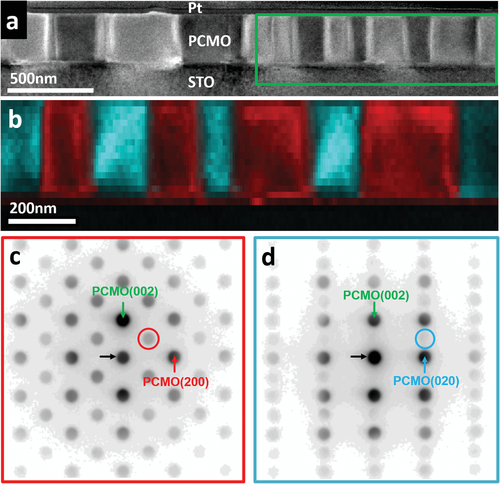
The XRD findings as well as high epitaxial growth quality is confirmed by the transmission electron microscopy (TEM) results, which were obtained with an STO[110] zone axis alignment throughout the entire manuscript: As shown in Figure 2 and expected for the relations (i) and (ii), the corresponding zone axis in the film is found to be either PCMO[100] or PCMO[010], that is, PCMO[001] is oriented out-of-plane in both cases. In fact, the in-plane orientation flips quite regularly on a few hundred nanometer scale and the resulting domains extend through the entire film as clearly visualized by the 4D-STEM analysis shown in Figure 2b–d. This reflects a nanotwinned state of the film as it is often observed in orthorhombic systems.[47, 48]
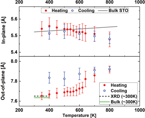
The temperature dependent lattice parameters obtained in the TEM and averaged over the upper half of the scanning field in Figure 2 are shown in Figure 3. The error bars represent the standard deviation in the averaged range. Noteworthy, the initial value of the out-of-plane lattice parameter, that is, PCMO[001], is consistent with the macroscopic XRD measurement presented in Figure 1c. Upon heating, the in-plane parameter, including contributions from PCMO[100] and PCMO[010], decreases with higher temperature. In contrast, PCMO[001] increases and is strongly hysteretic. The latter indicates an irreversible change of the TEM lamella during heating which is confirmed by a change in the crystal symmetry: Figure 4a,b shows series of NBED patterns of domains with PCMO[100] and PCMO[010] zone axis orientation, respectively. While in the former case a PCMO(00) superreflection emerges at 800 K, the PCMO(101) reflection vanishes in the latter. Both effects persist at lower temperatures after heating and in addition, the initially extinct PCMO(100) reflection shows up in domains with PCMO[010] zone axis orientation. The appearance of superstructures, although not exclusively occurring in one direction, has been reported before in the context of catalytical studies of PCMO (x = 0.36) and was attributed to oxygen vacancy ordering.[27] The circumstance that ordering is only observed along PCMO[010] might be related to the results in ref. [50] for x = 1 showing that in the presence of strain certain lattice sites are preferred for oxygen vacancy formation. Recalling the structural sketch presented at the bottom of Figure 1a, the emerging superstructure could be explained by oxygen vacancies occurring only at the oxygen site highlighted by a black circle but not at the site highlighted by a green circles. However, other configurations of oxygen vacancies are consistent with the observed superstructure along PCMO[010] and the change in extinction rules – being strongly linked to the tilt pattern of neighbouring MnO6 octahedra in stoichiometric perovskites[51] – suggests additional atomic reconfigurations. Noteworthy, the hysteretic increase of the out-of-plane lattice parameter in Figure 3 is qualitatively consistent with previously reported lattice expansion due to oxygen deficiency.[35]
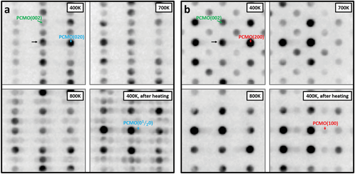
In order to suppress oxygen vacancy formation, an analogous experiment was conducted facilitating the environmental TEM (ETEM) gas-inlet capabilities and using an oxygen partial pressure of 10 Pa. The resulting lattice parameters obtained in the gaseous environment are shown in Figure 5. As a matter of fact, PCMO[001] still increases strongly with temperature but in contrast to the experiment in high-vacuum no significant hysteresis is visible. Furthermore, neither a PCMO(00) superreflection nor a change in the extinction rules was observed in the gaseous environment confirming oxygen vacancy formation to be directly linked to the previous irreversible changes.
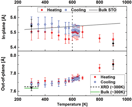
A striking observation is the sudden jump of the averaged in-plane parameter at 600 K during heating, which is not reverted during cooling. As a result, the averaged in-plane parameter approaches the lattice parameter of the substrate at that temperature proving its effect on the strain state of the PCMO. Bearing in mind that the PCMO films have been post-growth annealed at 1173 K this jump has to be attributed to the reduced thickness (≃100 nm) of the TEM foil along the electron beam direction, which permits further change of epitaxial strain. Following the curve after the jump reveals a reversible decrease of the averaged in-plane parameter at high temperatures. In fact, the black data points in Figure 5 (with the zone axis fine-adjusted at 900 K), which were acquired after the first heating cycle (with the zone axis fine-adjusted at 300 K), demonstrate that no significant irreversible changes are observed in the second cycle as well as that mistilt, for example, due to membrane bulging, does not hamper the interpretation of the presented lattice parameters.
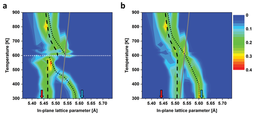
To disentangle the behavior of the so far averaged in-plane lattice parameters PCMO[100] and PCMO[010], the temperature dependent histograms of detected in-plane lattice constants during heating and cooling are shown in Figure 6a and Figure 6b, respectively. Please note that the histograms above T = 650 K in Figure 6b are re-plotted from (a). Generally, before and after heating, a bimodal distribution is observed at low temperatures and the two distinct peaks with lower and higher lattice parameter correspond to domains with PCMO[010] and PCMO[100] zone axis orientation, respectively. As the temperature is raised, the two peaks start to merge and a tetragonally-strained pseudo-cubic phase forms. It should be noted that the sudden jump during heating at 600 K discussed above occurs right at the pseudo-cubic transition in Figure 6a suggesting that isotropic lattice parameters are beneficial for this type of rearrangement. The temperature-dependent corresponding lattice spacing of bulk STO (solid gray line)[49] indicates an increased adaptation of the in-plane lattice parameters of the film to the substrate at 600 K. Furthermore, the arrows marking the room temperature bulk values of PCMO[100] (red) and PCMO[010] (cyan)[34] reveal increased tensile strain of PCMO[100] and decreased compressive strain of PCMO[010] at room temperature after heating. This again proves the epitaxial strain maintained by the substrate regardless of the thin foil effect discussed above.
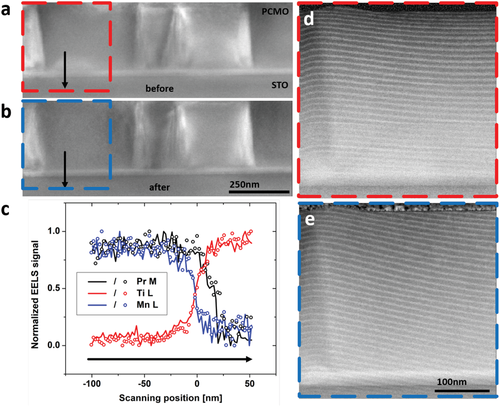
Despite the mentioned modifications of the strain state, no significant changes in size or position of the nanotwinned domains are observed: As presented in Figure 7a,b, the mesoscopic structure of nanotwinned domains is recovered after heating. Furthermore, it should be noted, that the Moiré patterns arising from the lattice resolution of the ADF-HRSTEM images in Figure 7d,e obtained at small magnification are a sensitive test for irreversible changes ruling out crack formation during the rearrangement. In addition, electron energy-loss spectroscopy (EELS) signals of the Pr M- (black), Ti L- (red), and Mn L-edge (blue) are provided in Figure 7c revealing chemical interdiffusion of Ti and Mn in the interface layer apparent by a bright contrast in Figure 7a,b, which is consistent with previous reports.[52] It should be noted that comparing the data before (lines) and after (open circles) heating excludes significant changes of the interdiffusion layer. Consequently, changes of the domain boundary nanostructure or of preparation-related point defect concentrations and variations in octahedral tilt are possible explanations for the structural modification.
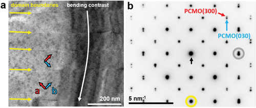
Although thin film strain relaxation phenomena are not in the focus of this study, some insight into the role of domain boundaries for the rather complex strain-stress state of the nanotwinned thin films is provided by Figure 8a,b, showing a plan-view TEM image and a selective area electron diffraction (SAED) pattern, respectively. There are two important observations, that is, (i) the domain boundaries indicated by yellow arrows in (a) tend to follow PCMO(110) and PCMO(10) lattice planes, and (ii) domains are strongly elongated in the horizontal and closely spaced in the vertical direction (note, that regions with the same arrangement but tilted by 90° are also observed but not shown here). As a third feature, lattice planes of the nanotwins parallel to the boundaries are aligned to each other while the planes perpendicular to the boundaries are canted as can be inferred from the split and overlapping peaks marked by a gray and yellow circle in Figure 8b. As the cross-sectional lamellas used in the in situ experiment where extracted along the diagonal direction in Figure 8a (yielding alternating PCMO[100] and PCMO[010] zone axis orientations), the elongated domains are cut at an angle of 45°. Thus, small rotations of the PCMO(110) and PCMO(10) lattice planes coinciding at domain boundaries—accompanied by defect formation—should be more favourable in the thin TEM foil compared with the macroscopic counterpart. Hence, the observed rearrangement at 600 K can tentatively be attributed to these small relative rotations in combination with expansion of the film along the electron propagation direction feasible in the TEM lamella. Notwithstanding these rather complex relaxation phenomena resulting from the nanotwinned microstructure, the orthorhombic to pseudo-cubic phase transition is observed in the thin film if heated up in an oxygen environment.
Finally, the results obtained in oxygen environment after the rearrangement shall be compared to bulk measurements. As described in ref. [34], a pseudo-cubic transition is expected in the bulk for x = 0.1 at ≈675 K. Our findings show that the transition occurs at a slightly lower temperature in the thin film, that is, at ≈600 K. Unfortunately, since no temperature-dependent lattice constants are published at this calcium concentration, we can compare the trends only qualitatively to the existing data obtained in the bulk for x = 0.[33, 36] Here, due to the pseudo-cubic transition at 1050 K, PCMO[001] increases by 3.8%, PCMO[010] decreases by 3.4 %, and PCMO[100] increases by 1.5 %. Since the initial anisotropy at room temperature is weaker for x = 0.1, it is to be expected that theses changes are smaller due to the increased calcium content matching very well the observed increase of PCMO[001] by ≈3.0% in Figure 5 and the decrease of PCMO[010] by ≈2.5% in Figure 6b. On the contrary, PCMO[100] behaves qualitatively differently as it decreases with temperature. Even though no direct comparison to the bulk can be drawn for x = 0.1, it seems very likely that this effect is rather caused by strain than by the finite value of x. We justify this claim with the fact that the increase of PCMO[100] is a fingerprint of the reduced MnO6 tilting angle having a stronger effect than the reduction of its JT distortion (which would in turn lead to an expansion in this direction). As the JT distortion is almost 50 % weaker for x = 0.1 at room temperature[34] and the tolerance factor, that is, the main driving force for octahedral tilts changes only by a few percent,[33] we do not expect a reverted behavior due to the increased calcium content and attribute the reverted trend to the anisotropic nanotwinned strain state.
3 Conclusion
In summary, nano-beam electron diffraction in combination with in situ heating in an environmental transmission electron microscope was used to study phase transitions in Pr1−xCaxMnO3 thin films epitaxially grown on SrTiO3 in the low-doping regime, that is, for a Ca concentration of 10 at%. The oxygen activity was varied by the oxygen partial pressure during the in situ experiment leading to two distinctly different routes followed by the system.
On the one hand, UHV conditions accompanied by oxygen loss and hence formation of oxygen vacancies in the thin film material. From the appearance of a PCMO(00) superstructure accompanied by a change in the extinction rules as shown in Figures 3 and 4, vacancy ordering can be concluded which persists after cooling to room temperature indicating a thermodynamically stable oxygen-deficient PCMO. We note here, that the observed anisotropy might be related to misfit strain resulting in an anisotropic oxygen vacancy formation enthalpy and formerly equivalent sites where oxygen vacancies could occur alternatingly along the PCMO[010] direction are marked by a black and green circle in Figure 1a.
On the other hand, 10 Pa oxygen partial pressure in the gaseous ambient inside the microscope column sufficiently reduces the oxygen loss and hence completely suppresses the hysteretic behavior of the out-of-plane lattice parameter PCMO[001], the change in extinction rules, as well as the superstructure formation. As a consequence, the clear detection of the reversible orthorhombic to pseudo-cubic phase transformation is possible with a slightly decreased critical temperature of ≈600 K when compared to the bulk counterpart.[34] In addition, a reverted behavior of the in-plane lattice parameter PCMO[100] was observed which was attributed to strain due to the cubic substrate and the mosaic-like microstructure of the films. It is quite interesting to note, that the irreversible relaxation occuring at about 600 K during the first heating ramp coincides with the pseudo-cubic transition shown in Figure 6a, that is, when the in-plane lattice parameters PCMO[100] and PCMO[010] are approaching lifting the strain relaxation due to the alternating twinned domains.
Finally, let us mention some implications of the results reported here. First of all, the study of phase transitions in thin film transition metal oxide perovskites by means of in situ electron nanobeam diffraction in 4D-STEM mode is an approach with several advantages over bulk diffraction studies. We have clearly demonstrated that controlling the oxygen activity by ambient conditions is not only a prerequisite for reliable in situ heating diffraction studies, but also possible in an environmental transmission electron microscope. This important conclusion can be generalized to other systems containing volatile components like nitrides and hydrides although details will depend on the properties of the specific system.
4 Experimental Section
A 400 nm thick PCMO film was grown on a commercial STO substrate with STO(100) surface termination by ion beam sputtering from a single target of composition (x = 0.1). Deposition parameters were: pAr = 3 × 10⁻² Pa (beam neutralizer), pXe = 1 × 10⁻² Pa (sputter gas), and pO = 1.6 × 10⁻² Pa (film oxidation). The deposition temperature was set to 820 °C using a Tectra boron nitride heater which results in ≈720 °C at the substrate surface. Subsequently, the film was annealed in air for 20 h at 900 °C with a ramping speed of 100 °C per hour.
TEM lamellas were extracted using an FEI Nova NanoLab Dual Beam focused ion beam and mounted on first generation four-contact DENSsolutions heating chips for the cross-sectional in situ experiment. For plan-view investigation, the preparation procedure described in ref. [53] was used. In both cases, the final thinning step was done using an acceleration voltage of 5 kV. TEM experiments were conducted in an FEI Titan ETEM G2 80-300 operated at 300 kV using a DENSsolutions Lightning D7+ holder and a semi-convergence angle of 0.8 mrad (NBED) and 10 mrad (HR-STEM), respectively. ADF-STEM images were acquired with an inner and outer collection semi-angle of 46.8 mrad and 200 mrad, respectively. EELS data was acquired with a Gatan Quantum 965 ER using a dispersion of 1 eV/channel under HR-STEM conditions and analyzed with HyperSpy[54] using the windows given in Table 2 for power-law background subtraction and signal integration.
| Edge | Background window [eV] | Signal window [eV] |
|---|---|---|
| Pr M | 870–920 | 920–1020 |
| Ti L | 395–345 | 445–495 |
| Mn L | 580–630 | 630–680 |
NBED patterns were recorded with a self-written DigitalMicrograph plugin controlling the beam position and reading out an UltraScan 1000XP camera binned to 256×256 pixels.
XRD was performed in a Bruker D8 diffractometer with a monochromated Cu Kα1 source.
Acknowledgements
The project was funded by the Deutsche Forschungsgemeinschaft (DFG, German Research Foundation)—217133147/SFB 1073, projects B02, Z02. The use of equipment in the “Collaborative Laboratory and User Facility for Electron Microscopy” (CLUE, Göttingen) is gratefully acknowledged. Furthermore, the authors acknowledge the open acces software VESTA,[58] which was used for grpahical illustration in Figure 1.
Open access funding enabled and organized by Projekt DEAL.
Conflict of Interest
The authors declare no conflict of interest.
Author Contributions
The design of experiments and their interpretation was the result of fruitful discussions including all authors. T.M. extracted the TEM lamellas from a thin film sample grown by B.K. and conducted the TEM experiments together with V.R. and B.K. The data was analyzed by T.M. under revision of M.S. The manuscript was written by T.M. under revision of M.S. and C.J.. All authors read and agreed on the written paper.
Open Research
Data Availability Statement
The data presented in this work can be found under: https://doi.org/10.25625/STJ0WN.


