The shapes of synthesized two-dimensional materials
Xiao Kong and Chengrui Fu contributed equally to this study.
Abstract
The shapes of as-grown/as-etched two-dimensional (2D) islands are the most recognizable features of the chemical vapor deposition (CVD) process which reveal a lot of information about the chemical environment of growth/etching, the effect of the substrate and the growth/etching kinetics. Here, we summarize experimentally observed shapes of CVD-grown 2D materials from previous reports, theoretical understanding on the corresponding mechanisms and the simulations of the corresponding growth/etching processes. Each part of the review article is organized by combining the fundamental principles that govern the shapes of crystals during growth/etching and the related experimental observations to facilitate the readers to read and understand the content. The content of the review includes attachment-limited 2D materials growth, diffusion-limited 2D materials growth (both with and without influence of the substrate), etching and merging of 2D materials with and without considering the effect of the substrate. We also discuss growth and etching of multilayered 2D islands during CVD—a topic still under development. We wish this review will also guide the audience to understand the kinetics of 2D materials growth and to improve controllable synthesis of various 2D materials.
1 INTRODUCTION
Two-dimensional (2D) materials have been attracting great research interest for several decades1-13 due to their potential applications in electronics,14-32 electrocatalysis,33-39 photocatalysis,40-45 sensors,46-52 and energy storage.53-56 Chemical vapor deposition (CVD) is the most mature technology for synthesizing high-quality, large area single crystal 2D materials. One of the ultimate goals of the growth process design is to efficiently control the properties of a material. These properties are determined by multiple factors, for example, the morphology, the number of layers, the type of exposed edges, and polycrystallinity.57-66 Although the desired morphology can be initially planned theoretically, the shape of as-grown samples may be influenced by symmetry of the substrate, strength of material-substrate interaction, as well as various experimental conditions.67 For example, in some reports on CVD growth of graphene, the as-grown graphene wafers showed stretched and truncated hexagonal, flower-like, snowflake-like or dendritic shapes, which were distinct from the expected regular hexagonal shape with six zigzag edges.68, 69 Such shape diversity results from specific experimental procedures, and therefore can be used to design better experiments and to manufacture devices with specific properties. It is worth mentioning that the CVD growth of 2D materials is even more complicated than that of three-dimensional (3D) materials. For example, interaction between the island and the substrate has a great influence on the shape of the island, which is not an issue in the 3D case. Despite the importance of understanding the shape of a 2D material during CVD growth or etching, there is still few review articles on the topic. In this study, we provide a comprehensive summary of experimental and theoretical research reported so far. Possible shapes of 2D materials including graphene, hexagonal boron nitride (h-BN), and transition metal dichalcogenides (TMDs) under different conditions are considered. This review will further help researchers to understand the shapes they observe in CVD growth and to improve quality of produced 2D materials.
2 SHAPES OF SINGLE-LAYER, SINGLE-CRYSTAL 2D MATERIALS
2.1 Procedure of CVD growth of 2D materials
To introduce formation mechanism of 2D materials, it is necessary to recall the procedure of CVD growth. Here we will use graphene as an example for a brief introduction.70-78 CVD growth of graphene generally contains three steps. First, the source of carbon (e.g., methane) is decomposed into carbon precursors (CH, CH2···) in the gas phase or on the substrate and is adsorbed onto the substrate. Then, the carbon precursors diffuse on the substrate until they nucleate as new graphene flakes or approach existing graphene flakes. Finally, carbon precursors react to form a graphene crystal. It should be noted that the growth procedure is different depending on the substrate. For example, in the case of copper, carbon precursor molecules directly form graphene on its surface, while in the case of nickel, carbon atoms can diffuse inside the substrate and then move on to the surface to form graphene.
The growth process is also determined by a distribution of precursors on the substrate which splits the CVD growth into two regimes: attachment limited growth and diffusion limited growth. If concentration of precursors on the substrate is so large that it can be considered constant everywhere, the growth regime is attachment limited. In this case, growth speed of the 2D material is determined by the final step of the CVD growth, that is, attachment of precursors to the edges of newly formed 2D crystals. On the other hand, at the diffusion limited growth, the concentration of precursors is low, so their diffusion becomes the dominant step determining growth speed of the material. Knowing the CVD growth regime determines the analysis of formation mechanisms of observed shapes.
2.2 Attachment limited growth without the influence of the substrate
If concentration of precursors is sufficiently large, then growth is attachment limited. This means that the growth of a 2D island is determined by reactions of precursors near the island edges. If the substrate is in the liquid phase or interaction between the substrate and the 2D material is extremely weak, growing 2D islands will have the shapes of regular polygons reflecting the symmetry of their crystal structure.79-89 Under such conditions, graphene grows into a hexagon, while h-BN and TMDs become triangles as their crystals have 3-fold symmetry. This is the simplest and the most ideal case. Formation of these shapes has been well understood and many approaches have been developed for shape prediction. This case also became the basis for understanding the shapes in more complicated situations.
It is widely known that when a crystal is in thermodynamic equilibrium, its shape can be predicted by the Wulff construction method stating that the shape of a 2D island is formed in such a way that the edge energy is minimized, and the ratio of the distance between its center and each edge is proportional to the corresponding edge energy. Artyukhov et al.83 calculated the energies of an armchair edge, , a zigzag edge, , as well as their self-passivating reconstructions on different metals. They obtained the equilibrium shapes of graphene on Fe, Co, Ni, and Cu according to the analytic formula , where is the angle of the edge from zigzag direction. It turns out that the shape of graphene on certain substrates is not hexagonal, and depends on the difference between the energies of zigzag and armchair edges.
Since kink nucleation usually has a higher barrier, it is the dominant factor influencing growth speed. Growth of highly-symmetric armchair and zigzag edges must start from a nucleation since these edges have no pristine kinks. Other tilted edges do have pristine kinks, so no kink nucleation is required for their growth. Therefore, these titled edges usually have larger growth rate than the highly-symmetric ones, and their growth rate is dominated by kink concentration. Specifically, an edge that has a 19.1° angle with a zigzag edge has the largest kink concentration, and thus has the largest growth speed among all edges of graphene.
Using kinetic Wulff construction, Ma et al.84 studied shape evolution of graphene during growth, reproduced here in Figure 1A–D. Active sites are marked in Figure 1A by different labels on several typical edges, and the illustration of KWC is shown in Figure 1B. Using DFT calculated zigzag and armchair nucleation energies, the predicted shapes of graphene islands grown on Pt (111) are shown in Figure 1D. The shape of a graphene island starts with a dodecagon having six armchair and six zigzag edges. Since armchair edges have a higher propagation speed, they gradually become shorter, and finally disappear in the next steps of the growth process. Then the final shape of graphene is determined by six zigzag edges with the slowest growth speed. Artyukhov et al.83 used KWC to predict the shape of graphene islands on other metal substrates. In Figure 1E, effective concentrations of three active sites on arbitrary edges are plotted, and nucleation barriers of zigzag and armchair sites calculated for several other metals are shown. Choosing a different chemical potential of carbon atoms, the shape of graphene on Ni(111) is predicted to have zigzag edges due to their slowest propagation rate.

As for h-BN and TMDs, their shapes under attachment-limited growth follow the same rules, but they differ from graphene in that TMDs and h-BN have two constituent elements. As a result, these 2D materials have two types of zigzag edges. A relative growth speed of zigzag edges may change with different experimental conditions. For example, GaSe has two kinds of zigzag edges which are terminated by Ga and Se atoms respectively, and will be called here ZZGa edge and ZZSe edge. Figure 1F shows the DFT-calculated formation energy profile of each type of edge of GaSe from Li et al.85 ZZSe has a larger formation energy than ZZGa, and thus has a lower growth speed when chemical potential between Ga and Se atoms, , is zero. Formation energy of the three types of edges as a function of is also shown in Figure 1F. It was found that the growth speed of ZZSe is larger than that of ZZGa if is larger than 0.15 eV. KWC results of the shape evolution during growth at = 0.06 eV and = 0.24 eV are shown in Figure 1G. A triangular island turns 180° when rises from 0.06 to 0.24 eV, which is consistent with the experimental results that the outer edges have been changed from ZZSe to ZZGa.
The triangular shape of GaSe in the last example shown in Figure 1G does not change but just turns by 180° as chemical potentials between Ga and Se changes. However, in many cases of CVD growth of h-BN and TMDs, truncated triangles may occur due to chemical potential between the two constituent elements. As shown in Figure 2A,87 the shape of an as-grown h-BN island can be tuned from triangular to truncated triangular, and then to hexagonal by decreasing the concentration ratio of nitrogen active species to that of boron on the substrate. Based on the edge passivation theory, Zhang et al.88 predicted the shape of h-BN at different temperatures and different chemical potentials of nitrogen, , with Wulff constructions and DFT calculations. The change of formation energy with respect to chemical potential and temperature for different edges of h-BN with different passivated structures is shown in Figure 2B. Figure 2C shows that the most stable shape without H-passivation is a hexagon with armchair edges, while Figure 2D shows the result with H-passivation at absolute zero and = 2.168 eV. Variation of shapes at a fixed temperature of 1300 K and varying is plotted in Figure 2E. When = 0.846 eV, the shape is triangular with zigzag-NH edges. As is increased, the three corners become increasingly truncated, so that the shape gradually changes from a truncated triangle to a hexagon. Further increasing leads to a 180° reversal of the truncated triangles which finally results in a triangle with opposite orientation from the initial one. This simulation explains various triangles and truncated triangles in CVD growth of h-BN. Similar variation of shapes triggered by chemical potential has also been observed for TMDs. Raju et al.89 studied different shapes of MoS2 islands by tuning chemical potentials of Mo and S. Their results are shown in Figure 2F–H, which are in a good agreement with Wulff construction in Figure 2I.
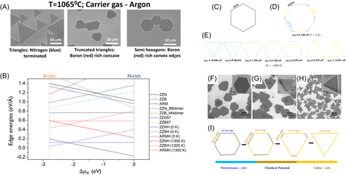
Without considering the effect of substrates, the shape of a 2D material grown at the attachment limit is mainly determined by its intrinsic structure and growth kinetics, which can be explained and predicted theoretically. However, for some 2D materials, the growth kinetics can be greatly modified by the growth environment. For example, Gu et al.90, 91 reported the growth of PdSe2 at different temperatures. At 600 °C, the PdSe2 nanosheets present “square-like” shape, which could be well predicted by the growth kinetics and the kinetic Wulff construction of PdSe2; at 500 °C, the PdSe2 nanosheets show “heart-like” shape. The “heart-like” shape neither obeys the symmetry of PdSe2 nor that of substrate, which implies that the nonhomogeneous growth environment or the complicate multilayer edge reconstruction play important roles during growth.
2.3 Detachment-limited etching
Research on etching of monolayer 2D crystals has also been reported.92-96 There are two types of etching observed in CVD: hole etching and island etching. During etching of 2D flakes, the edges with the fastest propagation speed gradually appear and eventually dominate the shape, which is a representative phenomenon for etching of 2D islands. As to the hole etching, the hole shapes are the same as the island shapes during growth. This implies that there is some relationship between growth and etching, which will be discussed in the next section.
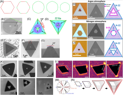
KWC is still a powerful tool to analyze shapes of etched 2D islands. Figure 3A shows the shape evolution of a graphene island during etching. Starting with a hexagonal shape with six zigzag edges, the island gradually becomes a regular dodecagon, after which it does not change its shape anymore. The dodecagon is terminated with twelve edges that are tilted by 19.1° to the zigzag edges and have the fastest propagation rate of all edges. Figure 3B shows the experimental observation of etched graphene, which is consistent with the simulation results. Figure 3C,D show KWCs of the GaSe etching. The 19° edge also occurs during GaSe etching, and the final shape of the island is terminated by six 19.1° edges. Figure 3E–G show SEM images of etched GaSe islands at different resolutions. Stehle et al.92 experimentally obtained microscopic and SEM images of h-BN islands after etching, as shown in Figure 3H–J, where different rows refer to different atmospheres. The as-etched islands have triangular outer shapes. The etched hole is a triangle with the same orientation as the outer triangle if buffer gas is argon. In nitrogen atmosphere, the hole is either a hexagon or a triangle with an opposite orientation to the outer triangle. Influence of an atmosphere on the shape of an etched hole is similar to that influence on the shape of 2D islands during CVD growth. It changes growth rate of different edges by chemical potential. The set of images in Figure 3K from Li et al.85 show shape evolution of a GaSe island during etching. The shape of an island is a triangle, and the etched hole also has a triangular shape but its orientation is different from a GaSe flake. Using in situ SEM, Sang et al.93 studied pattern variation of a Mo1−xWxSe2 hole during etching, as shown by the STEM images in Figure 3L. A hole starts from a diamond shape, and then turns into a triangle. The author also made a polar plot of the growth speed as shown in Figure 3M, from which we can see that there are two types of edges—ZZSe-NW-terminated edges and ZZMo-NW-terminated edges. The latter have a larger growth rate. KWC successfully reproduces the experimental observations on hole shape variation in Figure 3N.
2.4 Complementary relationship between shape evolution during growth and etching
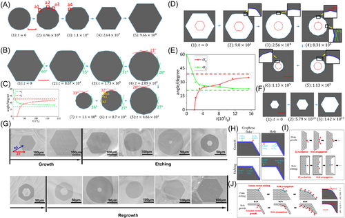
There is a complementary relationship between shape evolution during growth and during etching given that there is attachment limited growth, detachment limited etching, and no influence from the substrate. Using kinetic Monte Carlo (KMC), Kong et al.97 simulated growths and etching of graphene islands and holes. Figure 4A shows growth of a graphene island from a circular shape. As it grows larger, its shape first becomes a dodecagon terminated by six armchair edges and six zigzag edges. Then, the armchair edges gradually disappear due to their faster propagation speed. After the island becomes a hexagon with six zigzag edges, it stops changing its shape as it grows larger. Figure 4B shows the shape evolution during the etching of a graphene island. These simulation results are consistent with KWC. During etching, a dodecagon with the fastest 19.1° titled edges appears and keeps its shape as the island becomes smaller. Figure 4C shows change of angles and in the shape in Figure 4B. On the other hand, Figure 4D shows evolution of a hole during which its area becomes smaller. The hole starts from a hexagonal shape, gradually turns into a dodecagon, and then keeps decreasing in area while keeping its shape unchanged. The change of angles and in the shape in Figure 4D is shown in Figure 4E. It is interesting that this is similar to shape evolution during island etching. We find the same similarity if we compare shape evolution during island growth and etching of a hole, as shown in Figure 4F. Such complementary relationship has been verified by experimental graphene growth-etching-regrowth by Ma et al.84 reproduced here in Figure 4G. Detailed structures of parts of a graphene island and a hole near the corners are shown in Figure 4H. The text in these graphs illustrates reaction energies of corresponding events. Atoms at straight edges have the same number of neighbors for both islands and holes. Atoms at the corners of holes have more neighbors than atoms at straight edges, and even more neighbors than atoms at the corners of islands. Therefore, reaction energies for events at the corners of both islands and holes are larger than those at straight edges for both graphene flake growth and hole etching. Conversely, during graphene hole growth and island etching, reaction energies for events at the corners of both islands and holes are smaller than those at straight edges. This causes similarity between island growth and hole etching, as shown in Figure 4I, AND makes both of them complementary to the hole growth and island etching, as shown in Figure 4J.
2.5 Attachment-limited growth influenced by the substrate
Without the substrate's influence, all six zigzag edges of a graphene island have equal propagation speeds, leading to a hexagonal shape of the island. When the substrate cannot be neglected, its local atomic environments may cause unequal edge energies and nucleation barriers on the island edges. This makes growth rate of each edge different, and will break the original six-fold symmetry. A carefully prepared substrate can be used to remove the symmetry of 2D material growth, which leads to the epitaxial growth of 2D material single crystal.98-101 Besides that, propagation speeds of the island edges and therefore the island's shape may be affected by defects of the surface of the substrate.102
Artyukhov et al.103 investigated the shape of graphene on Ni(111) substrate. There are two stacking positions on Ni(111) surface: face centered cubic (fcc) and hexagonal close-packed (hcp) stacking. The six zigzag edges are also classified into two types: a normal zigzag edge and a Klein edge that has a dangling carbon atom. Artyukov et al.103 considered that graphene flakes can be not only on top of the surface but also inside the topmost plane. Edge energies in different cases are shown in Figure 5A, and Wulff constructions of graphene are plotted in Figure 5B. Free energy evolution during edge growth in fcc and hcp stackings for zigzag, Klein, and armchair edges are shown in Figure 5C,D. According to the calculated barriers, KWCs of graphene shape on fcc and hcp positions are shown in Figure 5E,F, respectively. We see that six-fold symmetry of graphene is broken, and graphene will grow into triangle islands on Ni(111) surface. Using similar methods, the shape of graphene on many other surfaces was predicted with Monte Carlo modeling, shown in Figure 5G. Most of these shapes have been observed experimentally.
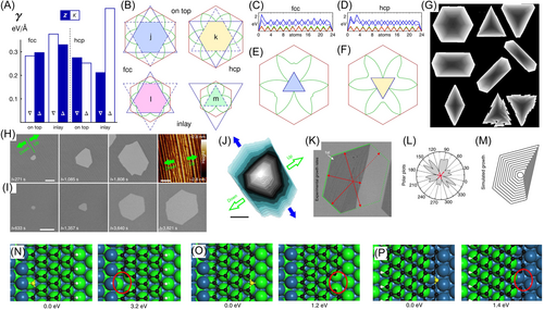
The presence of steps on a surface is another factor leading to change in symmetry.98-101, 104-107 In Figure 5H,I from Wang et al.106 the shape evolution of a hole on a faceted Pt surface is compared with that on a flat Pt surface during etching. The rightmost image in Figure 5H shows the direction of surface steps. A hole on a flat surface gradually turns into a hexagon, which is consistent with the previous section. However, a hole on an uneven surface becomes elongated in the direction perpendicular to the up/downward direction of the steps. This means that etching speed along the up/downward direction is suppressed. Wang et al.106 also experimentally observed the kinetic Wulff shape of graphene islands versus growth speed. Growth speeds in different directions of three layers of graphene were calculated according to the shape analysis shown in Figure 5K. Their polar plot is shown in Figure 5L. Growth speed along the up/downward-step direction is distinctly smaller than that in other directions. With growth speed fitted from experiment, the obtained shape from kinetic Wulff construction in Figure 5M is consistent with the experimental shape, which confirms that growth/etching speed of graphene domains is suppressed along the up/downward direction of surface steps. Furthermore, DFT calculations in Figure 5N–P show that upward-step etching requires a threshold energy change of 3.2 eV, and downward-step etching needs 1.4 eV, while the corresponding energy is only 1.2 eV on a flat surface. This explains the difference of growth/etching speed between the upward and downward directions along surface steps.
Analyzing the influence of a substrate on the shape of 2D materials, we made a general schematic diagram for possible shapes of 2D materials on four different types of surfaces, namely, (100), (110), and (111) surfaces of fcc metals as well as on h-BN(0001) surface. The materials we chose are graphene, FeSe, h-BN or TMD, and GeSe, which are typical 2D materials with six-, four-, three-, and two-fold symmetry, respectively. The alignment directions of these materials are taken into consideration according to previous studies, which show that a graphene zigzag edge prefers to be parallel to a lattice vector of Cu(111) surface. In the case of growing 2D islands on fcc(110) surface, which has one axis of symmetry, the shapes of graphene, FeSe, and GeSe are stretched along [100] direction of the surface. The reason is that growth speed of the edge in this direction has been greatly increased. For h-BN or TMDs, the intrinsic 3-fold symmetry leads to a triangular shape. Then, the 4-fold symmetry of fcc(100) surface changes the growth rate of 3 zigzag edges in two ways. If the zigzag edges with same termination still have the slowest growth rate, then the triangular shape of h-BN or TMDs will not change. Once the growth rate of one zigzag edge increases to a speed faster than that of the zigzag edge with opposite termination, the islands may become trapezoidal. Similarly, if the growth rate of 4 zigzag edges is faster than that of armchair edges, the graphene will become rectangular. On fcc(110) surface, which has two mutually perpendicular [100] directions, either [100] direction can be the one along which the island grows faster. Therefore, the final shapes of graphene, h-BN or TMD, and GeSe will be the same as that on (110) surface, with two mutually perpendicular directions. Besides that, 2D materials with four-fold symmetry represented here by FeSe remain rectangular because symmetry of the substrate is consistent with that of the 2D material. As for CVD growth on fcc(111) surface, graphene and h-BN remain hexagonal, TMDs are triangular, while 2D materials with four- or two-fold symmetry are stretched. Possible orientation directions are six (100) directions on (111) surface. On h-BN(0001) surface, which presents HPC structure with three-fold symmetry, zigzag edges of graphene can be divided into two groups. The difference of growth speed between the groups creates triangles or truncated triangles. The same difference between growth speeds makes the shapes of h-BN and TMDs truncated trapezoidal. The shapes of FeSe and GeSe are not influenced by the substrate. To summarize the possible shapes and alignments of different 2D materials on different surfaces, we have drawn a schematic diagram in Figure 6.
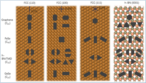
In addition to the symmetry of the substrate, the geometry of the substrate can also change the shape of the 2D material grown on it.108-110 Yu et al.108 theoretically and experimentally proposed that monocrystalline 2D material island grown on a conical surface can form a grain boundary with specific angle when it “catches its own tail” during growth. The tilt angle of grain boundary is decided by the conical angle based on the mapping from Cartesian coordinates to curvilinear coordinates. Zhao et al.109 furtherly demonstrated that a screw-dislocated WS2 multilayer island grown on a conical surface can bring supertwisted multilayer structures. Substrate geometry engineering must be a promising method for the controllable synthesis of 2D material wafers with specific structures.
2.6 Diffusion-limited growth without influence of the substrate
Attachment-limited growth/etching always occurs when the growth/etching rate of 2D material is slow and the precursors supply to the growth region is sufficient and uniform. In contrast, diffusion-limited growth happens if the supply of precursor is not uniform due to the diffusion rate of precursor during growth of 2D material. It is widely observed in the ultrafast growth of 2D material.111-123 Under such condition, the island's shape will be star-like, flower-like, dendritic or fractal. For example, the presence of oxygen can accelerate the growth rate of graphene on copper surface and lead to star-like graphene domains111, 117; high H2:CH4 ratio also can shift the growth kinetic of graphene from attachment-limited to diffusion-limited.123 These shapes usually reflect the original crystal symmetry. Employing phase field simulations, Zhuang et al.113 explored the mechanisms of forming these fractal shapes. In the phase field method, downward flux, , which represents the amount of incoming carbon atoms form CVD, and the diffusion coefficient, , are adjustable parameters. Figure 7A, B show the change of a graphene domain's shape and the concentration field with respect to these parameters, respectively. It has been found that the shape becomes more fractal as downward flux or the diffusion coefficient decreases. A semi-quantitative criterion to predict the final shape can be seen in Figure 7C. The shape can be classified according to the ratio between the size of depletion zone, , and the diameter of a graphene domain, . When , the shape is a regular hexagon. When , the shape is star-like. When , the shape is fractal, and when , we get dendritic shapes. With this concept, the experimental conditions can be adjusted. Hao et al.111 suggested that the presence of oxygen greatly reduces the growth barrier of graphene and therefore the diffusion coefficient is relatively lower. Xu et al.117 suggested that oxygen can also reduce the barrier of carbon species decomposition, which leads to an increase in downward flux, .
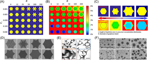
Two-dimensional materials of fractal shapes are often observed in experiments. Wu et al.68 performed CVD growth of graphene with different Ar:H2 ratios on liquid Cu surface and got various graphene flakes, eight of which are shown in Figure 7D. They clearly have fractal shapes. Each of these patterns corresponds to a certain pattern in Figure 7A. As the ratio of H2 increases, fractal behavior of the patterns also increases, changing from snowflakes to flower-like shapes with small dendrites, then to star-like shapes, and finally to hexagons with small convex parts. Figure 7E shows fractal patterns of h-BN islands grown at different temperatures on Cu-Si alloys obtained by Li et al.121 Fractal behavior of h-BN shapes is similar to graphene, only the symmetry is changed to three-fold. Similar fractal shapes have been found for TMDs122 as they also have three-fold symmetry. However, in the study of Huang et al.112 MoSe2 snowflake-like islands with six-fold symmetry were obtained, as shown in Figure 7F, which look like graphene fractal shapes. The reason that these MoSe2 show six-fold symmetry may result from the influence of the SiO2/Si substrate they used, making growth speed of six zigzag edges equal to each other.
2.7 Diffusion-limited growth influenced by the substrate
In an earlier section, we have discussed the influence of a substrate on the shape of 2D islands grown in the attachment-limited regime where the original symmetry of a 2D crystal may be broken, and its shape may be stretched. Due to surface steps, truncated shapes appear. Similar effects take place for fractal shapes in diffusion-limited growth where fractal shapes of low symmetry have been obtained.123-127
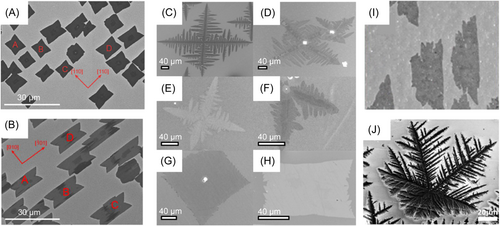
Figure 8A,B, taken from Deng et al.69 show graphene patterns on Cu(100) and Cu(110) surfaces, respectively. Graphene islands have fat bowtie shapes on Cu(100) and stretched bowtie shapes on Cu(110). The red arrows mark different directions of the surfaces; from which we can see how these graphene islands are aligned. Major growth directions will be those where zigzag edges of graphene have the largest speed due to influence of the substrate. That could explain the change of the graphene islands' symmetry. As Cu(100) has a four-fold symmetry and Cu(110) has a two-fold symmetry, graphene islands show two-fold symmetry on both surfaces. It seems that the patterns in Figure 8A,B are only slightly fractal. Jacobberger and Arnold123 performed APCVD and LPCVD growth of graphene on different copper surfaces and found more fractal behavior. Figure 8C–H show their major results on Cu(100) and (110) surfaces, in which the left column of images refers to Cu(100) surface and right column refers to Cu(110) surface. Different rows in Figure 8C–H correspond to different experimental conditions. We can see that graphene on these surfaces still shows two-fold symmetry but has dendritic shapes in Figure 8C–F, while it takes nearly regular shapes in Figure 8G,H. Similar shapes of graphene were obtained in experiments by Fei et al.126 In another study of Jacobberger et al.124 graphene islands on Cu(331) surface shown in Figure 8G have been grown. A fractal shape of a TMD is shown in Figure 8H; its formation is due to a great increase of growth speed along the bottom right directions. The symmetry of a surface is more complex on surfaces of a higher index, which causes more diverse change of graphene island shapes.
3 SHAPES OF SINGLE-LAYER POLYCRYSTALLINE 2D MATERIALS
3.1 Coalescence of polycrystalline islands
In Chapter 2, we mainly discussed shapes of monolayer single crystalline 2D materials. When initial nucleation sites are close to each other, the domains growing from these nuclei come into contact with each other. Depending on interaction between the substrate and the islands, many phenomena may occur during coalescence. If interaction is weak, one domain can rotate or shift slightly to make both grains have the same orientation and match their lattices, in which case these grains merge and become a single crystalline domain. When interaction between the substrate and the 2D material is strong, both grains cannot move. In this case, generally, a grain boundary will be formed during coalescence.128
Wang et al.128 systematically investigated differences in shape evolution of graphene domains on different surfaces and found that the type of coalescence of polycrystals can be predicted by observing the change of a concave corner between the islands. Figure 9A–D represents shape evolution of several graphene grains during growth on a weakly-interacting Pt substrate. At the beginning, the concave corner was 120°, while it gradually grew and a new 19° angle formed between the new and old edges. Figure 9E shows details of atomic models for shape variation for a concave corner between two graphene islands. Figure 9F–I show KWC results for coalescence of two graphene grains in four different directions. We see that coalescence of two well-aligned graphene domains initially leads only to formation of 60° or 120° concave corners. Then, these concave corners are filled by growing new 19.1° titled edges, and finally the grain becomes a stretched hexagon. Two sequences of SEM images in Figure 9J,K compare coalescence of graphene grains on Pt(111) and Rh(111) surfaces, respectively. It is clear that the concave corner on Pt(111) is filled quickly by growth of a newly formed edge, while that on Rh(111) surface remains unchanged. This comparison shows that a strong interaction between the substrate and the 2D material prevents formation of a single crystal.
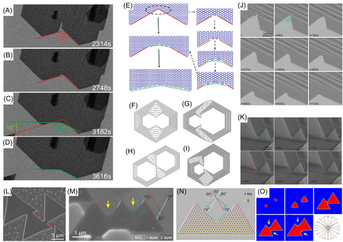
Forming a new edge at the concave corner during coalescence of 2D islands is not restricted to graphene but also exists for h-BN and TMDs. Figure 9L shows a SEM image of coalescence of h-BN domains on copper. The arrows mark rounded concave corners showing formation of new 19.1° edges. Figure 9M,N are an SEM image and atomic model showing the formation of a new edge during coalescence of MoS2 polycrystals on SiO2. Figure 9O presents phase-field simulation of shape evolution during coalescence of two MoS2 domains. These studies illustrate that formation of a 19.1° edge at the concave corner during merging of domains on weakly interacting surfaces is a common rule for all 2D materials.
Sometimes the edge of one domain can be lifted up to form a bilayer region with interlayer twisted angle during coalescence process. Yu et al.129 reported the coalescence behavior of monolayer MoS2. They found that when the misorientation angle , there tends to be a grain boundary in coalescence; when , edge of one domain tends to be lifted up to form a bilayer region. Further experimental and theoretical results reveal that the formation of bilayer region prevents the system from a long-range strain caused by the grain boundary. When misorientation angle , the strain is small and thus ploycrystals can be formed; when , the formation of grain boundary brings large strain in its vicinity, and thus MoS2 tends to form bilayer rather than polycrystals.
3.2 Shapes of polycrystalline 2D islands
If grains touch and coalesce into a single crystalline island, the island's shape can be predicted by kinetic Wulff construction and other methods. When multiple grains collide and form a polycrystalline island, grain boundaries appear between the individual grains.130-139 The most remarkable feature of polycrystalline islands is that their shapes have a number of concave corners.
Guo et al.130 showed both theoretically and experimentally that symmetrically tilted grain boundaries in graphene form straight lines, which are also the angle bisectors of the corresponding concave corners, and that grain boundaries in other 2D materials follow the same geometric rules. Besides that, misorientation angles of these grain boundaries have certain preferred values, which is convenient for predicting the shapes of polycrystalline 2D materials.
We can take CVD growth of graphene on liquid copper as an example. Figure 10A shows formation energy of a grain boundary versus its misalignment angle. The curve has two local minima located at 0° and 30°. Figure 10B shows two possible kinds of shape evolution of an island. When the misalignment angle of a grain boundary is very small, the grains become a single crystal. If the misalignment angle is around 30°, the grains form a polycrystalline island with a grain boundary between them. When the misalignment angle is 30°, it is possible to predict the shape of the final polycrystal. Using phase field simulations, Dong et al.131 showed that there are three possible shapes of graphene islands formed by coalescence of two grains. As shown in Figure 10C, the inner angle between the two concave corners should be , considering the symmetry of graphene. For the smaller of two grains, the only three possible combinations for the inner angle are 30°, 90° and 150°. Phase field simulations of shape evolution of polycrystalline islands formed by two grains are shown in Figure 10C. Shapes of polycrystalline islands formed by more than two grains are also predictable. The maximal number of grains in such polycrystalline islands is twelve. Dong et al.131 theoretically predicted 30 possible shapes of polycrystalline graphene and experimentally observed 27 of them. Most of these polycrystalline islands have star-like shapes with several small protruding parts.
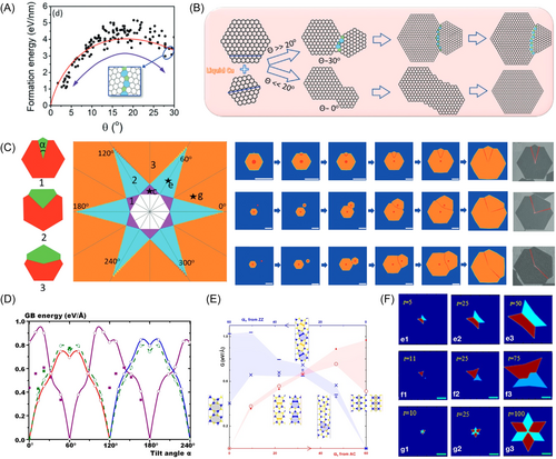
Liu et al.132 performed DFT calculations on energies of grain boundaries in polycrystalline h-BN islands with different tilt angles, as shown in Figure 10D. Zou et al.133 obtained the dependence of energy of a grain boundary in MS2 (M = W/Mo) islands on tilt angle. Their results are shown in Figure 10E. Grain boundaries in both h-BN and WS2 tend to have a misorientation angle of 60°. As in the case of graphene, their shapes can also be predicted. Using phase field simulations, Artyukhov et al.134 obtained bowties and David stars-shaped TMD polycrystalline islands (Figure 10F) by varying relative positions of initial grains. A bowtie-shaped island is formed by two grains with opposite orientation, while a David star shape is formed when four grains merge. Chen et al.135 also obtained these shapes with a KMC model. They also simulated formation of other shapes, such as five-pointed stars, and kite-like shapes.
The shapes of polycrystalline 2D materials on a solid substrate with specific symmetry can be classified based on growth orientations shown in Figure 6. Dong et al.136 explored the formation mechanism of polycrystals of various 2D materials on different substrates. In Figure 11A, all four possible shapes of polycrystalline 3-fold symmetric 2D materials on two-fold or six-fold symmetric substrates are listed and compared with experimental observations (Figure 11B). Figure 11C–F showed how to construct a possible polycrystal shape in a certain family. All possible shapes of 2D polycrystals in six families, namely III/II (3-fold symmetric materials on 2-fold symmetric substrate), III/VI (3-fold symmetric materials on 6-fold symmetric substrate), III/IV (3-fold symmetric materials on 4-fold symmetric substrate), IV/III (4-fold symmetric materials on 3-fold symmetric substrate), IV/VI (4-fold symmetric materials on 6-fold symmetric substrate) and VI/IV (6-fold symmetric materials on 4-fold symmetric substrate), were listed. There are four shapes in III/II or III/VI, 227 shapes in III/IV, 131 shapes in IV/III or IV/VI and 30 types in VI/IV. Many of them has been observed in experiments.
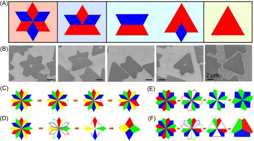
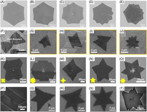
Figure 12 shows several experimental observations of polycrystalline 2D materials. Figure 12A–E show polycrystalline graphene islands from the study of Guo et al.130 who showed a total of 15 images but we provide only five of them here. According to phase field simulations of Dong et al.131 graphene islands in Figure 12A,B consist of two grains; the island in Figure 12C is formed by coalescence of four grains, and the islands in Figure 12D,E contain six grains. Shapes of h-BN polycrystalline islands are shown in Figure 12F–O. Figure 12F shows a typical bowtie-shaped h-BN polycrystal that has two grains with opposite orientations.138 Xu et al.139 produced other shapes of two-grain h-BN polycrystals with CVD on Co foils, shown in Figure 12G–I. They also obtained an eight-point star shape shown in Figure 12J. Figure 12K–O show the h-BN islands from the study of Ji et al.140 who obtained polycrystalline TMDs. Their possible shapes should be similar to those of h-BN islands because they both have three-fold symmetry. The shapes of two-grain polycrystals shown in Figure 12F–I are also common for TMDs. Figure 12P–T from the study of Zhang et al.141 show several images of polycrystalline WS2 islands that are similar to shapes of h-BN islands.
3.3 Etching of polycrystalline 2D islands
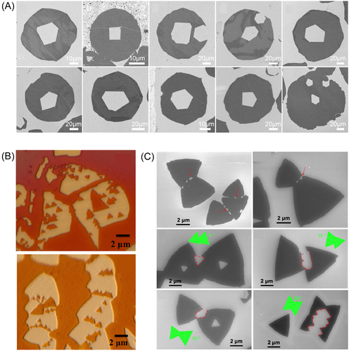
Etching of single crystalline 2D materials usually starts with point defects on them. Since a newly-formed hole has zigzag edges, it has the same orientation as the island. However, during etching of polycrystalline islands, their grain boundaries are also etched. Hence, there are two types of holes in polycrystalline islands. If a hole starts from inside the grain, all its inner angles are 120°. However, if the hole starts from a grain boundary, then not all its inner angles are 120°. If two etching holes start from the same grain boundary, and come into contact with each other, they form a trench separating the grains. Ten images in Figure 13A show an experimentally observed etching pattern of polycrystalline graphene islands.130 It is clear that the holes in the center of these islands have a few non-120° inner angles. Two images in Figure 13B show etching of h-BN,142 and six images in Figure 13C show etching of GaSe. In these images, we see both triangular holes and trenches between grains.85
4 SHAPES OF MULTI-LAYER 2D MATERIALS
4.1 Growth of multi-layer 2D materials
Although growth mechanisms of multi-layer 2D materials have not been systematically described so far, we can still discuss their shapes. One growth mode is interfacial nucleation, when a subsequent layer grows on top of or under existing layers depending on the substrate.143-148 Another mode is screw dislocation-driven growth, which results in several spiral layers with the same orientations.
Yan et al.143 synthesized a group of bi- and tri-layer graphene islands, as demonstrated in Figure 14A. The numbers in each image show orientation of each layer. 115 islands were investigated and half of them are bilayer and 30% of them are tri-layer islands. The remaining islands are monolayer and tetra-layer. The shapes of all these mono-, bi-, and tri-layer islands are hexagonal, therefore, it is clear that every layer of graphene is added under attachment-limited growth. Similar growth results have been obtained elsewhere.144 Li et al.145 synthesized bilayer graphene islands with the upper layer having a fractal shape. As shown in Figure 14B, except for the bottom right figure, the upper layers of the graphene islands have star-like or flower-like shapes. There are also reports on bilayer graphene with the bottom layer in a fractal shape and the top layer being a regular hexagon.146 All previously described graphene multi-layer flakes have been grown in an interfacial nucleation mode. There are also islands grown in a screw dislocation-driven mode. In the study of Tay et al.147 spiral graphene islands were obtained, as shown in Figure 14C. All layers in 2D polycrystalline islands have the same orientations and the same screw dislocations as their rotation axes.
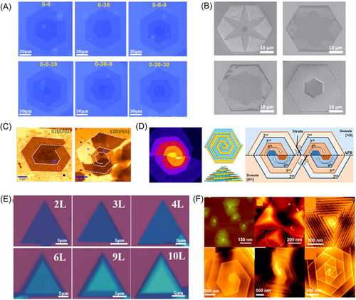
There are also multiple reports on multi-layer h-BN and TMDs.148, 149 Spiral growth of h-BN multi-layer islands can be seen in Figure 14D, IN which Park et al.148 displayed both an experimental image and a schematic diagram for its atomic structure. MoS2 multi-layer islands grown in an interfacial nucleation mode are shown in Figure 14E. The shapes of TMDs in a spiral growth mode can be found in the study of Shearer et al.150 who obtained three types of multi-layer WSe2 islands with different stacking structures, as shown by Figure 14F. The final shapes of the islands were triangular, truncated triangular, and hexagonal when the stacking structure was AA, AAB, and AB, respectively. Nie et al.151 performed phase field simulations to reproduce experimentally obtained shapes, and found that insufficient amount of chalcogen results in a concentric growth, while excessive amount of chalcogen leads to a spiral growth of TMDs.
4.2 Etching of multi-layer 2D materials
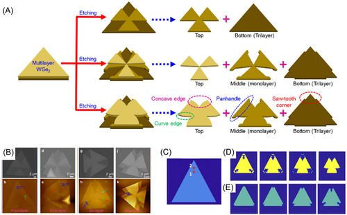
Etching of multi-layer 2D materials provides a way to design interesting devices with controllable properties.152, 153 There are papers reporting observation of kirigami structured multi-layer TMD islands obtained by etching.95 The overall shape of these islands is still triangular but the shape of each layer is different (Figure 15). Cai et al.152 reported a novel method to synthesize kirigami structured WSe2 islands by CVD growth and etching of multi-layer WSe2. Figure 15A shows a schematic diagram for the structures of three different multi-layer WSe2 islands. The upper, middle, and lower diagram has two, three, and four layers, respectively. We can see that complex morphology comes from stacking of different-shaped WSe2 monolayers.
5 SUMMARY AND OUTLOOK
We have given a systematic summary of shapes of 2D materials under different growth conditions observed during CVD growth and etching. Shapes of monolayer 2D materials are divided into several types based on different regimes: attachment-limited growth, diffusion-limited growth or etching, strong or weak material-substrate interactions, and monocrystalline or polycrystalline structure. Formation mechanisms of these shapes are understood and predicted by Wulff construction, kinetic Wulff construction, phase field simulations, and kinetic Monte Carlo. We also discussed shapes of multi-layer 2D materials, which is an on-going research with interesting potential applications in interlayer stacking, confined space growth, VDW heterostructures, and so on.
Shapes of as-grown/as-etched 2D islands provide insight into the CVD process. Compared to other features of CVD experiments, which are hard to monitor and control, the shape of 2D islands is the most recognizable feature which reveals much information of chemical environment during growth/etching. Observing the shapes of 2D islands, one can preliminarily estimate quality of the 2D material and know how strong the interaction between the material and the substrate is or if the amount of precursors is optimal. Based on the rules of shapes of 2D islands, the input ratio of gases, temperature, choice of the substrate can be tuned to improve quality of the 2D material and to explore novel phenomena of growth/etching. Therefore, deep understanding of the material shape is desirable in manufacturing 2D materials and their applications.
ACKNOWLEDGMENTS
The authors acknowledge support from the Institute for Basic Science (IBS-R019-D1) of South Korea.
CONFLICTS OF INTEREST
The authors declare no conflicts of interest.
Biographies

Xiao Kong is currently a research fellow in the Center for Multidimensional Carbon Materials (CMCM), Institute for Basic Science (IBS), Korea. He received his Ph.D. degree from the Beijing Normal University in 2018. His research interest is focused on the theoretical studies on growth mechanisms of 2D materials.
Chengrui Fu is currently a PhD student of Materials Science &Engineering department in the Ulsan National Institute of Science and Technology (UNIST). His research interest is focused on the theoretical studies on growth mechanisms of 2D materials.
Vladislav Gladkikh is a senior researcher in the Institute for basic science (IBS), South Korea. He received his Ph.D. from the Weizmann Institute of Science in 2007. His research interests include mathematical modeling, machine learning, density functional theory, and molecular dynamics for 2D materials.

Feng Ding is a Distinguished Professor of Ulsan National Institute of Science and Technology (UNIST) and a group leader of the Center for Multidimensional Carbon Materials (CMCM) of the Institute for Basic Science (IBS), South Korea. After receiving his Ph.D. from Nanjing University in 2002, he has worked with Gothenburg University of Sweden (2003–2005), Rice University of USA (2005–2008), and Hong Kong Polytechnic University (2009–2017). His research team at UNIST is interested in computational method development, theoretical exploration of various carbon materials and 2D materials, especially their formation mechanism, the kinetics of their nucleation, growth and etching.


