Chemo-mechanical polish lithography: A pathway to low loss large-scale photonic integration on lithium niobate on insulator
Summary
We discuss the recent breakthrough in the field of photonic integrated circuits for generating high-quality photonic structures on lithium niobate (LN) on insulator (LNOI). This is enabled by the development of chemo-mechanical polish lithography (CMPL). We begin with a brief introduction of the background, followed by the description of the CMPL technique that holds the promise for realizing LNOI waveguides of ultralow propagation loss approaching the absorption limit of LN. We demonstrate fabrication of low loss optical waveguides with the CMPL and construction of beamsplitters with the fabricated LNOI waveguides. At last, some conclusions and future perspectives will be given.
A video abstract of this article can be found at: https://youtu.be/sgnecU_QzcY
Video Abstract
Chemo-mechanical polish lithography: a pathway to low loss large scale photonic integration on lithium niobate on insulator (LNOI)
by Wang et al.1 INTRODUCTION
Electronic integrated circuits (EICs) are widely recognized as the workhorse of the modern information society. The capability of integration of a huge number of tiny transistors into small chips leads to ceaseless growths of the computational power and information processing rate in the past decades. Inspired by such great success, miniaturization and integration has become a trend in many areas other than electronics, such as chemistry, medical and photonics, to name a few.1-3 In particular, the photonic integrated circuits (PICs) are expected to play the leading roles in the future optical communications and optical information processing, both of which are currently dominated by the optical systems constructed by assembling the bulk optics.4, 5 The stability and scalability are the main bottlenecks for the sustainable development of complex optical systems aiming at high functionalities. PIC provides a solution to these challenges.
It seems straightforward to realize PICs in a similar way of realizing the EICs.6-8 The optical lithography is a mature technology that can now provide a resolution down to a few nanometers. Considering the photons in the visible and near-infrared (NIR) wavelength ranges, the nanometer-scale fabrication resolution appears to be sufficient for realizing high-quality PICs of which the feature sizes are limited to micrometer scale due to the diffraction limit. However, the optical lithography can often leave behind a surface roughness of a few nanometers on the sidewalls of the fabricated photonic structures, which causes undesirable scattering losses.9 In addition, the optical lithography was originally designed for realizing the EICs on semiconductor materials. Unfortunately, most semiconductor materials cannot have all the ideal optical properties at once as required by the PIC applications, such as a broad transmission window as well as high nonlinear optical and electro-optic coefficients. Thus, it is highly in demand to develop innovative PICs on some other material platforms. One candidate is the crystalline lithium niobate (LN).10
From the material point of view, LN is almost perfect for PIC application. It has a broad optical transparency window (0.35 μm-5 μm), a high nonlinear coefficient (χ(2) = 30 pm/V), a high refractive index (∼2.2), and a large electro-optical effect (r33 = 30.8 × 10⁻¹² m/V).11, 12 The recent development of the LN on insulator (LNOI) makes it possible to realize planar LN nanophotonic structures of configurations similar to the EICs on silicon.13 It should be noted that the fabrication of LNOI nanophotonic structures exclusively relies on ion beam etching, as the crystalline LN cannot be easily patterned with the traditional optical lithography due to its high chemical stability.14-19 The ion beam etching inevitably leaves behind a surface roughness on the order of a few nanometers, which limits the ultimate Q factor of a freestanding LN microdisk to ~106. The problem has recently been resolved by first patterning a chromium (Cr) thin film coated on the top surface of LNOI into a hard mask with a femtosecond laser, followed by the chemo-mechanical polish (CMP) for structuring the LNOI into the microdisk.20, 21 We will show below that the CMP lithography (CMPL) can enable ultrahigh performance LNOI photonic structures, opening the venue toward large scale, low loss, reconfigurable PICs for numerous applications. The performance of on-chip integrated photonic structures has approached that of the bulk optics fabricated in traditional ways such as polishing and coating. The landscape of photonic integration may be fundamentally changed from now on.
2 TECHNICAL DETAILS OF CMPL
The CMPL can potentially be used for patterning various kinds of dielectric materials. Nevertheless, at this moment, only LNOI has been tested as a platform material for photonic applications with the CMPL. The LNOI wafer is provided by NANOLN (NANOLN, Jinan Jingzheng Electronics Co, Ltd, Jinan, Shandong, China), which is formed by bonding an LN foil of a thickness ranging from a few hundred nanometers to approximately one micrometer onto a layer of fused silica of 2 μm thickness. The LN foil is produced using ion slicing technique. The backside of the fused silica is directly bonded onto a piece of bulk LN substrate of a thickness of 500 μm to form the LNOI wafer.
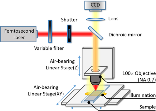
The CMPL includes four major procedures, as illustrated in Figures 1A to 1D. First, a thin layer of chromium (Cr) with a thickness ranging from 600 nm to ∼1 μm was deposited on LNOI by magnetron sputtering. The thin layer of Cr serves as a protection mask once being patterned by either laser ablation or optical lithography.20, 21 Second, the Cr foil will be selectively removed with a high spatial precision using femtosecond laser ablation. The advantage of femtosecond laser ablation is that the short pulse duration enables nonthermal interaction between the laser pulses and material, making it possible to achieve clean and sharp ablation free from the influence of heat diffusion.22 As a metal, Cr can strongly absorb laser light that gives rise a relatively lower ablation threshold than LN as the latter is a dielectric material of a large bandgap. Therefore, one can take this advantage to choose a peak intensity of the femtosecond laser at which the Cr film can be completely removed while the underneath LNOI remains intact. In this step, as shown in Figure 2, the femtosecond laser system provides a femtosecond laser beam with a central wavelength of 1028 nm and a pulse duration of 170 fs. During the Cr patterning process, the repetition rate is adjusted to match the scanning speed by a build-in computer-controlled pulse picker. The laser power is finely tuned with a variable neutral density filter. A single-blade optical beam shutter is used to synchronize the femtosecond laser ablation and the translation of the stages. A short-pass dichroic mirror reflects the femtosecond laser beam into a 100× objective of a high numerical aperture (NA, 0.7∼0.8) to obtain a tightly focused spot with a diameter of ∼1 μm. The objective was installed on an air-bearing linear stage with a translation resolution of 100 nm to control the position of the focal spot along Z direction. Femtosecond laser ablation was performed by translating the LNOI sample with a computer-controlled XY air-bearing motion stage at a translation resolution of 100 nm. The motion range of the XY stage is 200 mm in the X and Y directions. In the femtosecond laser patterning of Cr, the focal spot was scanned line by line with a spacing of 0.8 μm (ie, smaller than the focal spot size) to generate a clean LNOI surface without any remaining Cr. A charge coupled device (CCD) camera was installed above the objective lens to monitor the fabrication process.
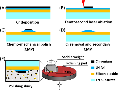
Next, the CMP is carried out using a wafer polishing machine. The tiny LNOI sample is embedded in a resin that is encapsulated in a retaining ring with a saddle weight as shown in Figure 1E. The polishing pad is a piece of velvet polishing cloth. Amorphous colloidal silica suspension is chosen as the polishing slurry, and the diameter of the silica particle is 60 nm. The soft texture of the velvet cloth ensures the polishing slurry to be accessible by the exposed LN foil even the top surface of LN foil is slightly underneath the top surface of the Cr mask. Since the hardness of the Cr film is much higher than that of the LNOI, the exposed LNOI can be completely removed after the CMP process and the patterns defined by the Cr mask will be faithfully transferred to the LNOI. By carefully controlling the duration of the CMP process, the side wall angle with respect to the vertical direction can be controlled from a few tens of degrees to nearly 80°. The next step is to remove the Cr mask by immersing the sample in a standard Cr etching solution for 10 minutes. In this case, the entire layer of Cr can be completely removed. However, in case one would like to keep some parts of the Cr on the LNOI that can be used as microelectrodes, the Cr can also be removed in a space-selective manner using the femtosecond laser ablation. At last, an additional CMP (ie, the secondary CMP) needs to be conducted for further smoothening the upper areas of the sidewall. Since the upper areas of the sidewall of the patterned LNOI are close to the Cr mask, these areas will inherit the sidewall roughness of the Cr mask generated by the femtosecond laser ablation. This problem is resolved by thinning the LNOI with the secondary CMP until the rough areas near the top surface are completely removed. For waveguide-based applications, the secondary CMP is of critical importance as it can ensure the extremely high smoothness for the entire surface of the waveguide.21
3 FABRICATION OF LOW LOSS WAVEGUIDE
An LNOI waveguide fabricated with the CMPL is shown in Figure 3. From the top view micrograph, it can be seen that the waveguide is highly uniform as any variation of the width along the waveguide is hardly visible (Figure 3A). As shown in the cross-sectional micrograph of the waveguide as presented in Figure 3B, the waveguide appears narrow on the top with a width of ∼1 μm and become wider near the bottom with a width of ∼4 μm. This trapezoidal cross section of the waveguide is a typical feature of CMPL whereas the trapezoid angle can be controlled to some extend by adjusting the saddle weight as well as the polishing duration.
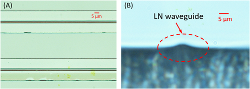
Figure 4A shows another LNOI waveguide fabricated by the CMPL of which the width of the top surface is only 0.7 μm. The narrow width is achieved by optimizing two experimental conditions. First, the femtosecond laser ablation is conducted with extreme care to obtain the narrowest width on the ablated Cr mask. Afterwards, the polishing duration must be controlled in a precise way to avoid over polishing; otherwise, cracking and fracturing can often occur. Nevertheless, the result in Figure 4A reveals that, by refining and strictly controlling the fabrication conditions, waveguides of sub-micrometer width can readily be fabricated using the CMPL. Thus, the achievable mode-field size with the CMPL, which is a technique based on optical fabrication, will be comparable to that obtained with the electron beam lithography (EBL) or ion beam lithography, owing to the ultimate limit on the mode-field-size of single-mode propagation.
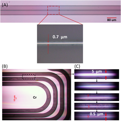
Figures 4B and 4C show that, with the increase of polishing duration, the Cr mask can be gradually removed beginning from the two lateral sides and progressing toward the middle area. In our experiment, the LNOI samples are polished by hands, which cannot ensure a sufficient reliability and reproducibility. Thus, to reduce the influence from the uncertainty caused by the hand polishing, the width of the waveguides is chosen to be >1 μm in the construction of the photonic structures in the current stage. It is noteworthy that, if the CMPL can be implemented in an automatically way without the involvement of handcrafts, it is expected that much finer waveguides will be produced in a reliable and reproducible way.
The optical loss of the LNOI waveguides is expected to be low with the CMPL. From the above discussion, all the surfaces of the waveguide have undergone the mechanical polish. The mechanical polish is known to be able to provide extremely high-quality optical surfaces. Actually, we have measured the top surface roughness of the waveguide with an atomic force microscope and obtain a root-mean-square surface roughness of 0.452 nm.21 The surface roughness is sufficiently good for many optical applications, which, however, can still be improved in the future as, in principle, a surface roughness on the order of 0.1 nm should be achievable with the CMP process. For an optical waveguide with a low loss well below 0.1 dB/cm, the loss cannot be precisely measured with the cut-back method unless the waveguide can be made with a meter-scale length. This is impractical for an optical waveguides fabricated on a tiny chip. Therefore, the waveguide loss is obtained by measuring the Q factor of a waveguide ring resonator as described elsewhere.21 An ultralow optical loss of 0.027 dB/cm has been achieved.
4 CONSTRUCTION OF BEAMSPLITTER WITH THE LNOI WAVEGUIDES
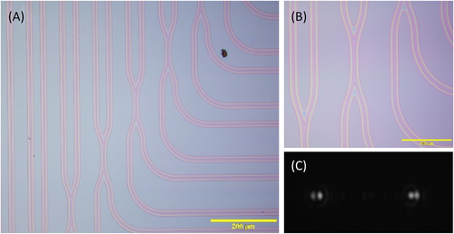
The waveguide has been used for constructing optical beamsplitters. Figures 5A and 5B show a group of beam splitters composed of waveguides with a width of 1 μm. In the coupling area, the two arms merge into one arm with a greater width. Coupling of the light waves has been confirmed by observing the exiting beams from the two output ports. However, we found that the splitting ratio of the two exiting beams is unstable, which is sensitive to how we couple the beam into the beamsplitters. This is due to the fact that the waveguides shown in Figures 5A and 5B can support not only single-mode propagation but also propagation of some high-order modes. As shown in Figure 5C, the second-order modes are clearly seen from the two output ports after the light beam have traveled through one of the beamsplitters. Similar second-order modes have been observed in all of the beamsplitters in Figure 5A, indicating that the LNOI waveguides of a width of only 1 μm can support propagation of both the first- and second-order modes due to the high refractive index of crystalline LN. Further reducing the width of the waveguide is possible but will lead to much worse reliability and reproducibility in the fabrication of long waveguides, as we have discussed above. Moreover, for waveguides of very small mode field sizes (ie, much less than 1 μm), the coupling efficiency between the waveguides and standard single-mode optical fibers will be low.
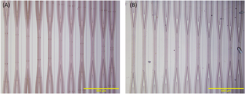
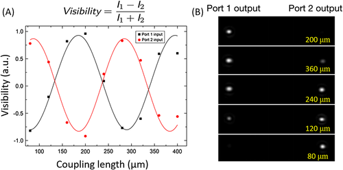
To overcome the problems in the fabricating single-mode LNOI waveguides with the CMPL, we redesign the LNOI waveguides by covering them with a layer of Ta2O5, as shown in Figure 6. In the new design, the LNOI waveguides in the beamsplitters all have a width of 1.5 μm as shown in Figure 6A, which is far from the requirements for the single-mode propagation in a bare LNOI waveguide. The LNOI beamsplitters are entirely covered with a layer of Ta2O5 of a thickness of 4 μm, as shown in Figure 6B. As Ta2O5 has a refractive index of ∼2.05 which is close to the refractive index of LN, single-mode propagation has been observed in the waveguides in Figure 6 (see, the inset of Figure 6B). In the experiment, a beam at 1550 nm wavelength was coupled into the beamsplitters using a fiber lens. The polarization of the input beam was controlled using an inline fiber polarization controller. The output beam profiles were imaged with an NIR camera using a 20× objective lens. A polarizer was inserted between the objective lens and the NIR camera to allow only transverse electric (TE) mode to pass through. The power of the output beam was determined by integrating the grayscale intensity over the entire area of the near-field beam profile captured by the NIR camera. The visibility is defined as (I1 − I2)/(I1 + I2). Here, I1 and I2 are the powers of the exiting beams from the two output ports, respectively. A clear sinusoidal dependence of the beam-splitting ratio on the length of the coupling area has been observed as shown in Figure 7. The beamsplitters are the building blocks for constructing Mach-Zehnder (MZ) interferometers that are the key components for various PIC applications.
5 CONCLUSIONS AND FUTURE PERSPECTIVES
We have shown that the CMPL provides the solution to achieve an extremely high surface quality of sub-nanometer roughness, which is hardly accessible by other lithographic approaches such as the optical lithography, EBL and ion beam lithography. The capability of generating the extremely smooth optical surfaces with the CMPL can be easily understood from the well-known fact that the CMP is a well-established technique for fabricating bulk optical components of an excellent surface finish. The fusion of optical lithography and CMP inherits the advantages of both technologies, including the high fabrication efficiency, high fabrication resolution, large footprint size, and low optical loss. Applying CMPL on LNOI leads to tunable PICs. Although we focus on LNOI in the current work, in principle, a large variety of materials can be patterned with high surface quality by the CMPL once the materials can be prepared in the form of a thin foil lying on the bulk substrates.
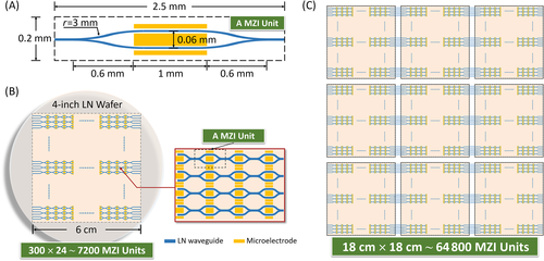
The results described above provide ample information for us to draw the roadmap of LNOI-based PICs. Here, let us consider a specific example that is representative for a large number of applications. The PIC device considered here is constructed by arranging as many LN MZ interferometers as possible into a grid array on a single LNOI wafer. Technically speaking, since 4-inch LNOI wafer is already commercially available, we will consider building the abovementioned MZ interferometer array in a square-shaped area of 60 mm × 60 mm footprint size as allowed by the 4-inch wafer. As for a single MZ interferometer, the arm length is limited by the requirement to generate a phase shift of π in an electric field whose strength is below the coercive field threshold (∼20 kV/mm) of the LN crystal.23 The shortest arm length can thus be determined to be ∼1 mm. With the demonstration of the single-mode LNOI waveguides buried in Ta2O5, the minimal radius of curvature at the bend is calculated to be ∼3 mm (ie, the bending loss is completely negligible under this condition). If we assume that the two arms in the interferometer should be separated by 0.1 mm to avoid the cross talk associated with the eletro-optic tuning, it can be derived that the footprint size of an individual MZ interferometer on the LNOI can be as small as 0.2 mm × 2.5 mm as shown in Figure 8A. Thus, a photonic device composed of 7200 MZ interferometers as schematically shown in Figure 8B will be readily achievable with the CMPL. The total propagation loss in such a large-scale PIC device is estimated to be well below 0.5 dB, and may be further reduced to below 0.1 dB if the surface smoothness can be improved by finer CM polish. Furthermore, for the femtosecond laser microfabrication system used in our experiment, the range of motion of the stage is 20 cm × 20 cm. Thus, we should be able to tile 9 pieces of LN photonic chips on which the entire PIC device is patterned at once in a continuous processing manner. The alignment between the different chips is automatically secured with the continuous patterning process. The total number of MZ interferometers on the tiled LN chip can reach 64 800. For such a large PIC device, the ultralow loss in the waveguides is critical for achieving a satisfactory performance.
The perspective given above suggests that LNOI-based PICs offers the potential for efficient and fast on-chip manipulation of a large number of quantum states, which is highly desirable by quantum information processing. Functional components and devices that could be enabled by the LNOI PICs include quantum light sources, high precision interferometers, multidimensional quantum entangled system, programmable quantum logic gates, quantum key distributors, and quantum simulators such as quantum chips for Boson sampling and random walk, to name only a few.11, 24-33 More than that, the potential of realizing large-scale, low loss, tunable PICs on LNOI opens up the possibilities in optical computations and communications, metrology, microwave photonics, and optical interconnection.34-36
ACKNOWLEDGEMENTS
This work is supported by the National Basic Research Program of China (grant 2018YFB0504400), by the National Natural Science Foundation of China (grants 11822410, 11874154, 11874375, 11734009, 61761136006, 11674340, 61675220, 61590934, 61575211, 61505231, and 11604351), by the Strategic Priority Research Program of Chinese Academy of Sciences (grant XDB16000000), by the Key Project of the Shanghai Science and Technology Committee (grants 18DZ1112700 and 17JC1400400), by the Shanghai Pujiang Program (grant 18PJ1403300), by the Shanghai Rising-Star Program (grant 17QA1404600), by the Shanghai Young-Talent Program (grant 1601031F30), by the Key Research Program of Frontier Sciences, Chinese Academy of Sciences (grant QYZDJ-SSW-SLH010), and by the Foundation of Youth Innovation Promotion Association (grant QCH-2018-8).


