Tuning Crystallization Pathways in Ge-Rich GST Alloys: The Influence of Nitrogen and Hydrogen
Abstract
This study investigates the effects of nitrogen and hydrogen doping on the crystallization mechanisms of Ge-rich GST (GGST) alloys, widely used in phase-change memory applications. Using in situ synchrotron X-ray diffraction, transmission electron microscopy, Fourier-transform infrared spectroscopy, and thermal desorption spectroscopy, this article examines undoped, nitrogen-doped, and co-doped (N + H) GGST samples to understand their structural and kinetics transformations during thermal treatments. Nitrogen doping significantly increases the crystallization temperature and enhances thermal stability, while reducing grain sizes and modifying kinetics. Hydrogen shows a contrasting effect. Alone, it minimally impacts crystallization temperatures but decreases activation energy and promotes heterogeneous nucleation, mediated by transient GeTe Pnma phase. However, combined with nitrogen, hydrogen disrupts the formation of GeN bonds, favoring NH interactions instead. This suppresses nitrogen effects while introducing interface-driven crystallization mechanism. The findings provide new insight into dopant interactions within GGST alloys, demonstrating the potential of co-doping strategies to fine-tune phase change behavior. The study underscores the need for further exploration of dopant combinations to achieve enhanced stability and performance, particularly for memory devices operating in harsh environments.
1 Introduction
Phase change materials (PCMs) are a class of functional materials that, over the past 40–50 years, have been used to develop data storage media in the form of optical drives (CDs, DVDs, Blu-ray disks, etc.),[1] and later as memory devices driven by electrical pulses for reading and writing (phase change random access memories, or PCRAM).[2-4] The principle behind the use of these materials is their ability to exist in at least one crystalline structure and one “metastable” (with a lifespan of several decades) amorphous structure. These two forms exhibit significantly different optical properties (used in optical disks) and electrical properties (used in PCRAMs), which can be assigned digital “1” (SET state/crystalline) and “0” (RESET state/amorphous). Furthermore, the structural state of a PCM region can be quickly switched (≈100 ns) at nanoscale by applying localized optical (laser) or electrical (via Joule effect through a conductive heater) pulses of different duration, enabling efficient memory writing. Among the PCMs, the ternary compound Ge2Sb2Te5 (GST225) is the most common and prototypical materials.[5] It offers several advantages compared to other competitors, however, its relatively low crystallization temperature (≈150 °C)[6] negatively impacts the stability of the amorphous phase and, ultimately, the expected data retention time (especially when operating in harsh environments).
Better thermal stability or device performances can be achieved by optimizing the composition, for example, by adjusting the Ge/Sb/Te ratio or adding new dopants. By enriching with Ge, the so-called Ge-rich GST alloys (GGST) have been found to have a significantly increased crystallization temperature up to 380 °C,[7] allowing PCM devices based on GGST to achieve better stability at higher temperature and enhanced device performances.[8-10]
From the perspective of doping, several publications have explored a wide range of elements, especially light elements, including Si,[11] Al,[12] Mg,[13] O,[14, 15] N,[15-18] C,[19] Bi, Sn, In,[20] B,[21] Ga,[22] Ti,[23] Se,[24] and rare earth.[25] C- and N-doping significantly improve thermal stability, whereas other doping element, such as Ga, stabilizes the fcc phase. Overall, doping fine-tunes GST's crystallization, thermal stability, and electrical performance, advancing its suitability for PCRAM applications. Notably, elements such as Na, Ne, F, Be, Li, and He have not been used due to manufacturing challenges, including toxicity, cost, or extreme chemical reactivity. To our knowledge, however, the effects of the lightest element, hydrogen, have yet not be investigated.
The Ge-rich GST alloys undergo a significantly intricate and multistep crystallization process, each influenced by the thermal budget (time, temperature), composition, and doping.[26-29] This process unfolds as follows, with increasing thermal input: (1) phase separation occurs within the amorphous phase, creating Ge-rich and Ge-poor domains;[26, 30] (2) small Pnma GeTe crystals nucleate, initiating the heterogeneous crystallization of Ge within the layer;[31] (3) a cubic GST phase forms, which is not the stoichiometric GST225 but rather cubic GeTe.[32] At this stage, Ge and GeTe crystalline grains remain embedded in an amorphous, Te-rich matrix that contains the majority of the Sb atoms; and (4) complete crystallization of GGST is achieved only by annealing above 400 °C, resulting in the formation of cubic GST225 along with some Sb-rich trigonal phases.[32] Introducing nitrogen primarily affects the kinetics of the entire mechanism.[16, 17, 27, 30, 33] It enhances the thermal stability, reduces diffusivity, and improves both electrical and structural properties of Ge-rich GST, making it a promising strategy for advancing phase-change memory technologies. These changes result from nitrogen's ability to form bonds with Ge during the diffusion path of Ge, and alter crystallization dynamics.
In this work, we aim to explore the effects of hydrogen doping, both alone and in combination with nitrogen, on a Ge-rich GST alloy. To evaluate such effects, four different families of samples were prepared: undoped GGST (referred to hereafter as REF, as a reference), nitrogen-doped GGST (GGST_N), hydrogen-doped GGST (GGST_H), and hydrogen-plus-nitrogen-doped GGST (GGST_NH).
These four sample families were studied using a variety of characterization techniques, including in situ X-ray diffraction (XRD) using synchrotron radiation, in and ex situ transmission electron microscopy (TEM) with chemical analysis using electron energy loss spectroscopy (EELS), in situ thermo-desorption (TDS), as well as ex situ optical characterizations such as Fourier-transform infrared spectroscopy (FTIR).
2 In and Ex Situ Characterizations
2.1 In Situ Ramp Annealing: Phase Sequence and Crystallization Temperatures
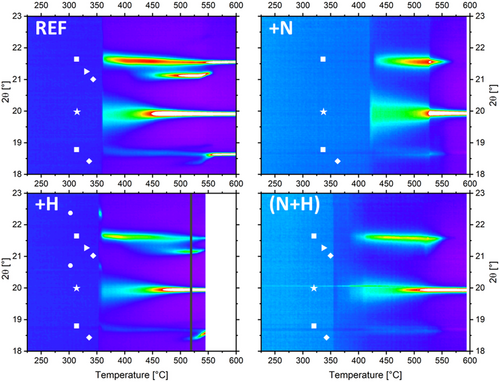
The four samples, namely, undoped (REF), N-doped (GGST_N), H-doped (GGST_H), and (H + N)-doped (GGST_NH) were characterized using in situ synchrotron XRD, during ramp annealing at 2 °C min−1, to determine both phase sequence and crystallization temperature (Tx). The results are shown in Figure 1 (see also Supporting Information Figure S1 and Figure S2 for full diffraction patterns and peak identification). All the samples exhibit the cubic Ge and GST fcc phase, whereas trigonal GST phases are detected only for REF and GGST_H samples, and the transient GeTe Pnma phase[31, 34] is only clearly detected for GGST_H. Regarding the phase sequence during the multistep crystallization process, although the trigonal phases are more or less visible over the probed temperature range—depending on the sample and its crystallization temperature—the overall phase sequence remains the same as that reported in the literature for undoped GGST:[31] whatever the doping, Ge crystallizes first, clearly preceded by GeTe Pnma phase for GGST_H, and followed by GST fcc. At higher temperatures, and for REF and GGST_H samples, trigonal phases appear.
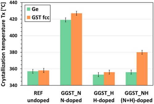
The in situ data were fitted using a multiple-peak model to extract each peak's intensity, width, and position. Additionally, some random datasets (with different doping and annealing conditions) were analyzed using Rietveld refinement (not shown here, see e.g., ref. 29) to validate the results obtained with the multiple-peak model approach. Crystallization temperatures (Tx) were extracted from fitted data for both Ge and GST fcc phases, considering the first temperature at which each phase appears. These results are shown in Figure 2. For undoped and N-doped GGST (REF and GGST_N), both Tx values align with those reported in the literature.[16, 17, 28] As expected, the Ge crystallization temperature for undoped GGST is ≈357 °C, while N-doping significantly increases it (up to 419 °C). In contrast, H-doping alone has a negligible effect on both Ge and GST fcc crystallization temperatures. However, the effect of double H + N doping is striking: adding H to GGST_N reduces TxGe back to its undoped value while inducing a longer delay between the crystallization of Ge and GST (TxGST-TxGe = 25 °C in GGST_NH, compared to ≈8 °C in GGST_N). This makes this sample the only one to exhibit a substantial difference between the two Tx values.
2.2 In Situ Isothermal Annealing: Kinetics, Grain Sizes, Lattice Parameters, and Activation Energies
Several in situ isothermal annealing experiments were performed between TxGe-30 °C and TxGe for each sample. Figure 3 presents the evolution of the normalized integrated intensities (proportional to the crystallized volume) over time during isothermal annealing at TxGe for Ge, GST fcc, and GeTe Pnma phases when detected. As reported in literature, N-doping slows down the overall crystallization kinetics.[17] Regarding H-doping, Figure 3 clearly demonstrates that H affects the kinetics only when N is present. For H-only doping, the kinetics are very similar to those of undoped GGST. In contrast, for GGST_NH, the kinetics are slower compared to GGST_N. Specifically, a greater time lag in the onset of crystallization is observed, along with a different evolution of the Ge signal, which appears much less abrupt. Instead of a nucleation-only profile as in GGST_N, the Ge signal in GGST_NH, follows a pattern more characteristic of nucleation and growth. Indeed, in the case of GGST_N, the integrated XRD intensity of Ge reaches its maximum almost instantly. This behavior—along with the absence of grain growth shown in Figure 5 for this sample—is typical of a nucleation-driven process, where grains form quickly but do not grow, resulting in a constant diffracting volume reached right away. In contrast, for GGST_NH, the XRD intensity increases gradually. Combined with the grain growth observed in Figure 5 for this sample, this suggests a process where nucleation is followed by grain growth, leading to a progressive increase in diffracting volume and, consequently, in integrated XRD intensity. Additionally, a distinct irregularity (indicated by the arrow in Figure 3) is observed at the onset of Ge crystallization. These findings are corroborated by the data in Figure 4(a) which show the crystallization onset times for Ge and GST, at TxGe, for all samples. In summary, 1) H impacts the crystallization kinetics only when N is present; 2) for H-only doping, the kinetics and crystallization times are very similar to those of undoped GGST, with however a slight increase in the time required for crystallization; and 3) with H + N doping, the kinetics are significantly slower compared to N-only doping, with an increased crystallization time and a larger delay between the crystallization of Ge and GST. These differences are also confirmed for isothermal annealing at lower temperatures (see Figure S3 in Supporting Information). At these temperatures, the evolution of the integrated intensities of the GeTe Pnma and GST fcc phases is more visible. As previously described by Rahier et al.[32] these phases are closely linked: GeTe Pnma grains transform in favor of the GST fcc phase, whose stoichiometry is initially poor in Sb during the early stages of crystallization.
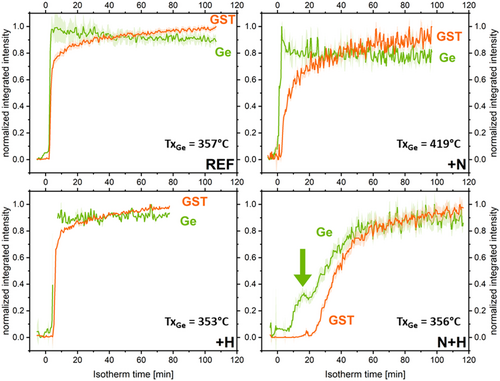

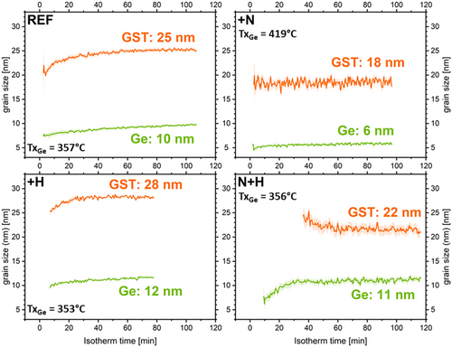
Figure 5 shows the evolution of average grain size for both Ge and GST fcc phases, during isothermal annealing at TxGe. These grain sizes were determined using the integral breadths of the diffraction lines, neglecting microstrain contribution. For REF sample (undoped), the average grain size of Ge remains almost constant, with only a slight growth of less than 10%, corresponding to the nearly constant crystallized volume (see Figure 3). In contrast, small grain growth is observed for the GST fcc phase, with an increase of ≈25%. As expected, for N-doped GGST, almost no grain growth is observed, and the grain sizes for both Ge and GST fcc are smaller. This is consistent with the known effect of N-doping, which renders crystallization more “nucleation-dominated”,[18] and reduces grain size.[17] The effect of H-doping depends on whether it is introduced alone or in combination with N-doping. When applied alone (GGST_H), the behavior is very similar to undoped GGST, with slightly larger final grain sizes for both Ge and GST fcc (≈16% larger), and minimal grain growth for GST fcc. However, when H-doping is combined with nitrogen (GGST_NH), the final grain sizes for Ge and GST are similar to those of undoped GGST. Notably, Ge grain size increases significantly at the beginning of isothermal annealing, indicating some grain growth up to ≈40 min, which corresponds to the observed increase in Ge integrated intensity (see Figure 3).
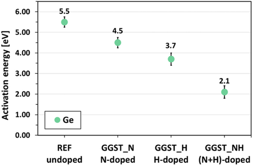
Both Equation 2 and Equation 4 lead to the same relationship between time and temperature, described by Equation 3. This equation was used to extract the activation energy for Ge crystallization across all samples (see Supporting Information Figure S4). The results are presented in Figure 6. For undoped GGST, the activation energy is approximately (5.5 ± 0.25) eV. N-doping reduces this value by about 1 eV, while the presence of hydrogen alone lowers the activation energy by roughly 2 eV compared to the undoped sample. When both dopants (N and H) are present, the activation energy is significantly reduced to ≈2 eV.
2.3 Ex Situ Analyses: Microstructures, Grain Compositions, and Bonding
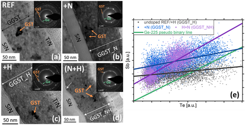
Ex situ TEM analysis was conducted on all samples after isothermal annealing at TxGe for 80 to 120 min (see Figure 3). In addition, some in situ TEM analyses were performed on (N + H)-doped GGST, as shown in Supporting Information Figure S5. Figures 7(a–d) presents the TEM results (bright-field (BF) images and corresponding selected area electron diffraction (SAED)) of the four samples. In all cases, both Ge and GST fcc are detected, with grain sizes consistent with those determined from XRD analyses (see Figure 5): GST grains consistently remain larger than Ge grains across all samples. N-doping reduces grain size, whereas H-doping does not significantly alter the overall microstructure. Furthermore, Figure 7(d) reveals that the lower interface (with the SiN underlayer) of the (N + H)-doped GGST layer is highly rough, with GST grains predominantly localized in the upper part of the layer. These observations were corroborated by in situ TEM analysis (see Supporting Information Figure S5): for (N + H)-doping, Ge crystallization begins at the bottom interface of the GGST layer, in the region close to the H source, where the H concentration is expected to be maximum (see Figure S5 and Figure S7), and propagates upward through the layer. In contrast, similar analyses of undoped and N-doped samples show homogeneous crystallization throughout the GGST layer.[17, 32] Figure 7(e) illustrates the local compositions of GST fcc grains as determined by EELS analysis. As previously reported for undoped GGST (REF), the cubic GST phase exhibits an average composition that is Sb-poor, with an Sb/Te ratio close to 0.1, indicating a composition approaching GeTe. For this characteristic, the behavior of H-doped GGST closely resembles that of undoped material. Introducing N-doping results in a slight increase in the average Sb/Te ratio, suggesting that more Sb is incorporated into the GST grains (though it should be noted that the isothermal annealing temperature was higher due to the elevated TxGe in N-doped GGST). Finally, in the case of (N + H)-doped GGST, despite having a TxGe similar to that of undoped GGST, the Sb/Te ratio is significantly higher (≈0.45). The composition points form a straight line parallel to the one connecting Ge and GST225, but are offset upward toward Sb. This indicates that substantially greater amount of Sb is incorporated into the cubic GST phase in (N + H)-doped samples compared to other samples.
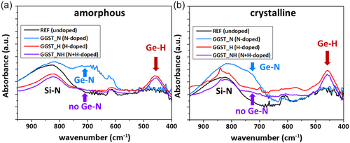
FTIR analysis was performed on all samples, both in their amorphous (as-deposited) and crystalline states (after isothermal annealing at TxGe for 80 to 120 min, depending on the samples, see Figure 3). The results are shown in Figure 8, with the Si substrate signals subtracted from the spectra and baseline correction applied. The peak around 620 cm−1, visible in almost all samples with varying intensity depending on the neighboring peaks, is likely due to the TiN capping layer and corresponds to TiN stretching mode.[37, 38] The measurements are similar for both amorphous and crystalline layers. For all samples, regardless of the structure (amorphous or crystalline), a broad peak at about 830–860 cm−1 is observed, characteristic of the SiN underlayer film and associated with an SiN asymmetric bond-stretching mode.[39-41] In the H-doping sample (GGST_H), an additional peak appears around 470 cm−1, attributed to the GeH wagging mode,[42] indicating the presence of GeH bonds in the H-doped GGST layer. In the N-doped sample (GGST_N), a distinct absorption band is detected around 730 cm−1, assigned to the in-plane asymmetric stretching vibration of the Ge3N skeletal group,[27, 43] indicative of GeN bonds in the N-doped GGST layer. This peak shifts to higher wavenumbers in the crystalline state, as previously reported by Prazakova et al.[27] This shift is due to a gradual rearrangement of Ge and N atoms, particularly linked to a depletion of Ge around the main GeN vibration. In contrast, when H-doping is combined to N-doping (GGST_NH), this absorption band disappears, suggesting that H suppresses or reduces GeN bond formation. However, in this sample, the peak corresponding to the GeH wagging mode remains present, confirming that GeH bonds are preserved. NH bond signatures were however not detected. As discussed later (see Section 3.2 and Supporting Information Figure S6), only diazene (N2H2) and hydrazine (N2H4) were detected in the GGST_NH sample through thermodesorption experiments. These molecules exhibit very weak stretching mode peaks in the 3000–3500 cm−1 range, which were not detectable. Finally, for both H-doped samples (GGST_H and GGST_NH), the presence of Sb-H bonds cannot be excluded. Such bonds would typically produce peaks around ≈782 cm−1 and ≈827 cm−1.[44] However, these signals are likely obscured by the broad SiN peak at 830–860 cm−1, preventing definitive identification.
3 Discussion
3.1 Transient Pnma GeTe Phase
As described by Rahier et al.[31, 32] the transient Pnma GeTe phase nucleates just before Ge in undoped GGST, triggering the heterogeneous nucleation of Ge at relatively low temperatures (below ≈360 °C, as shown in Figure 2). This occurs below the temperature at which homogeneous crystallization of Ge typically begins (≈380 °C).[45] For undoped- and doped-GGST layer, and for various annealing condition (ramp and isothermal annealing), Table 1 summarizes the occurrence of the transient Pnma GeTe phase. As expected, for undoped and N-doped GGST, the transient Pnma GeTe phase does not form during annealing above 350 °C, meaning it is absent under all annealing conditions used for N-doped GGST. However, in H-doped GGST, even though TxGe is similar to that of undoped GGST, the Pnma GeTe phase appears during isothermal annealing up to TxGe+ 2 (corresponding to 355 °C), and during ramp annealing as well. This indicates that heterogeneous crystallization triggered by the transient GeTe phase is favored in the presence of H alone. The presence of H, which forms GeH bonds (see Figure 8) and possibly SbH bonds (see Section 2.3), may promote phase separation, facilitating GeTe bonding and, consequently, the nucleation of the Pnma GeTe phase.
| Sample | TxGe (°C) | Ramp (2 °C min−1) |
Iso TxGe-30 |
Iso TxGe-20 |
Iso TxGe-10 |
Iso TxGe |
Iso TxGe + 2 |
Iso TxGe + 5 |
|---|---|---|---|---|---|---|---|---|
| REF undoped | 357 | ✓ | ✓ | ✓ | ||||
| GGST_N (N-doped) | 419 | |||||||
| GGST_H (H-doped) | 353 | ✓ | ✓ | ✓ | ✓ | ✓ | ✓ | |
| GGST_NH (N + H-doped) | 356 | ✓ |
When both doping elements (N + H) are present, the transient GeTe Pnma phase appears only at TxGe-30, despite TxGe being very similar to that of undoped GGST. In this sample, however, heterogeneous Ge crystallization is triggered by the SiN/GGST interface (see Section 2.3 and Supporting Information Figure S5). This interface-driven mechanism allows for the initiation of Ge crystallization without requiring the transient GeTe phase.
3.2 Interactions between Dopants and GGST Elements
FTIR analysis (see Figure 8) has shown that introducing H into N-doped GGST (GGST_NH) reduces or suppresses GeN bonds. A logical hypothesis is that this favors the formation of NH bonds. Indeed, NH bonds have a strong bond energy of ≈4 eV, compared to ≈2.7 eV for GeN bonds. Additionally, the formation enthalpy of the GeN system is about −0.25 eV/at (Ge3N4 structure),[46, 47] while that of the NH system is also relatively low, ranging from ≈−0.085 to −0.04 eV/atom).[48]
Thermodesorption experiments were performed on the GGST_NH sample using the protocol previously described.[49] The results, shown in Supporting Information Figure S6, reveal that during the main desorption event -corresponding to the disappearance of the GST diffraction peaks-[49] several NxHy molecules, mainly diazene (N2H2) and hydrazine (N2H4), are released from the (N + H)-doped GGST layer. This finding confirms the hypothesis that when both dopants are present, N preferentially bonds with H rather than Ge, explaining the disappearance of the GeN bond signature in the FTIR spectra for this sample.
The effect of H-doping is thus closely linked to the presence of N-doping. In samples without N, H preferentially bonds with Ge (and/or Sb), resulting in minimal changes to the GGST crystallization process, with the same phase sequence and similar kinetics observed. In contrast, in sample already containing N, H preferentially bonds with N, suppressing the effects of N-doping (e.g., increased Tx, smaller grains, slower kinetics) by preventing GeN bonds.
3.3 Activation Energies
As shown in Figure 6, the activation energy (Ea) for Ge crystallization in the N-doped GGST layer is reduced to 4.5 eV compared to 5.5 eV for undoped GGST, even though the crystallization temperature (TxGe) is higher. In this alloy, Ge crystallization occurs only after phase separation in the amorphous phase.[32] Consequently, the Arrhenius equation used to extract Ea reflects the diffusion process of Ge atoms within the GGST matrix. Interestingly, although TxGe differs significantly between undoped and N-doped GGST (ΔTxGe = 62 °C, see Figure 2 and Table 1), Ge crystallization occurs after the similar annealing times (see Figure 4(a)). Considering that Ge crystallization is triggered when the material is at the same stage of phase separation, with or without N, this suggests that the diffusion coefficients at these two different temperatures are comparable. Nitrogen reduces the activation energy for diffusion, making it more likely for Ge atoms to “jump” and diffuse, but it also reduces the average distance traveled between successive jumps. As a result, more jumps are required to cover the same distance, which can be achieved by increasing the temperature. Nitrogen appears to decrease the cohesive energy of GGST (and hence the “average” binding energy of Ge) while simultaneously increasing the density of traps, such as dangling bonds or N-terminated chains.
With H doping only, TxGe is almost the same as in undoped GGST (see Figure 2 and Table 1), but the activation energy is lower (3.7 eV, see Figure 6), and the time for Ge crystallization is only slightly longer (see Figure 4(a)). This implies a slightly lower diffusion coefficient at the same temperature for H-doped GGST. Considering the form of the diffusion coefficient , reducing the Ea implies decreasing the pre-factor D0 to obtain a lower diffusion coefficient. In this sample, GeH (and/or SbH bonds) are detected (see Figure 8). Without N, no GeN are present and N does not slow down the kinetics. One explanation for this lower Ea with H only would be a more probable Ge diffusion process with H, with however smaller distance between two jumps, due to GeH bonds, and H acting as traps for Ge. The smaller Ea could also be linked to the nucleation of the GeTe Pnma transient phase in most of the isothermal annealing (i.e., whatever the temperature up to TxGe + 2) for this sample, the GeTe Pnma phase providing heterogeneous crystallization sites for Ge.
Finally, in the (N + H)-doped sample, TxGe remains almost the same than in undoped-GGST (see Figure 2 and Table 1), but the time for Ge crystallization increases significantly (see Figure 4(a)), while the activation energy decreases further to 2.1 eV, this value being less than half that of N-doped GGST. In this sample, GeN bonds are not detected, NH bonds are indirectly observed (see Supporting Information Figure S6), and GeH (and/or SbH) bonds may also be present. Ge nucleation is shown to be heterogeneous, with the first nuclei forming at the bottom damaged interface with SiN, followed by Ge diffusion and crystallization toward this interface. The reduced activation energy in this sample is likely a combination of heterogeneous nucleation facilitated by the damaged SiN interface and the presence of GeH bonds, which may further reduce the energy barrier for Ge diffusion and crystallization.
Finally, although the annealing ramps or isothermal annealing conditions do not match the timescale of switching operations in real PCRAM devices, the activation energy of such experiments can be used to explore the temperature dependence of the crystallization at higher temperatures. By extrapolating Equation (3), which relates the variation of ln(Δt) to , one can estimate the temperature above which Ge crystallization could be triggered in less than 1 μs, the time scale at which PCRAM memory cells operate. This extrapolation was performed, as an example, for the undoped GGST (REF) sample (see Supporting Information Figure S8). The results indicate that this can be achieved at temperatures above 475 °C, i.e., significantly lower than the melting points of Ge or GST.
3.4 Overall Crystallization Process
The combined results indicate that the multistep crystallization process and phase sequence previously described for undoped GGST[32] are generally preserved across all doping conditions. Phase separation in the amorphous phase, driven by Ge diffusion, leads to Ge crystallization (preceded by the formation of the transient GeTe Pnma phase at sufficiently low temperatures), followed by the crystallization of the GST fcc phase. At higher thermal budgets—which are significantly elevated in the case of N-doping—the trigonal phases emerge. However, the crystallization temperatures for the Ge phase increase significantly with N-doping (+62 °C), but remain nearly unchanged in H-doped and (N + H)-doped GGST compared to undoped GGST. Overall, H doping suppresses the effect of N-doping.
When applied alone, H-doping has a modest impact on the kinetics, but significantly reduces the activation energy (Ea) by ≈1.8 eV, likely due to the formation of GeH and/or SbH bonds. GeH bonds may promote the formation of the transient GeTe Pnma phase, which triggers heterogeneous Ge crystallization throughout the layer, and reduces the activation energy. Meanwhile, SbH bonds could delay the overall crystallization process compared to undoped-GGST by further slowing Sb diffusion. This effect would delay the incorporation of Sb into cubic Sb-poor GST, thereby postponing the formation of Sb-richer GST phases.
When combined with N, H does not change the phase sequence but essentially changes the beginning of the crystallization process: TxGe is reduced by ≈60 °C compared to N-doped GGST and heterogeneous nucleation occurs at the bottom interface with SiN that is damaged. Such mechanism induces Ge diffusion to the bottom of the layer, then its crystallization mainly in the bottom part of the layer. This heterogeneous nucleation probably also explains the distinct irregularity (indicated by the arrow in Figure 3) observed in the integrated XRD intensity of Ge Bragg reflection at the onset of crystallization, and the higher delay between Ge and GST crystallization in this sample (see Figure 2 and 4(a)). In the upper part, with a lower Ge concentration, GST crystallization occurs with a composition closer to a “Ge-rich GST225” (Sb/Te ≈ 0.4), together with the remaining Ge. Both the heterogeneous crystallization of Ge and the lower Ge concentration in the top part of the layer explain the lower measured TxGe, and the longer delay between Ge and GST crystallization. NH bonds have been indirectly evidenced (FTIR, TDS) together with the reduction of GeN bonds (FTIR): contrary to N-doped GGST, almost no N is incorporated in Ge crystals (XRD) when H is present. The much lower activation energy for crystallization (down to 2.1 eV) can be explained by both the heterogeneous nucleation and the presence of GeH bonds. NH bonds induce the reduction of GeN bonds, and could promote phase separation in the amorphous state, and finally the same order of magnitude measured for the overall crystallization process (with (N + H) and in undoped GGST), after long isothermal annealing.
4 Conclusion
The influence of N- and H-doping (combined or alone) on the crystallization process of Ge-rich GST has been studied using in and ex situ characterization experiments (XRD, TEM, TDS, and FTIR). This study highlights the intricate roles of nitrogen and hydrogen dopants in tuning the crystallization pathways of Ge-rich GST alloys. While nitrogen doping significantly enhances thermal stability, crystallization temperature, and grain refinement, hydrogen, when combined with nitrogen doping, introduces a unique interplay by altering the crystallization kinetics and phase evolution: hydrogen effectively suppresses the effects of nitrogen (which is due to GeN bonds), favoring NH interactions and heterogeneous nucleation mechanisms. The findings reveal that hydrogen reduces the activation energy for Ge crystallization, facilitating diffusion-driven processes, while disrupting the benefits typically associated with nitrogen doping, such as improved thermal stability. The synergistic yet antagonistic effects observed in (N + H)-doped samples underscore the nuanced role of hydrogen alone in modifying the structural and kinetic properties of Ge-rich GST. These insights not only advance the fundamental understanding of dopant interactions in Ge-rich GST systems, but also pave the way for tailoring phase-change materials to achieve optimal performance for PCRAM applications. Future investigations focusing on the interplay of dopant concentration, thermal budgets, and bonding will be crucial in harnessing these effects for industrial and technological advancements.
5 Experimental Section
100 nm-thick GGST and N-doped GGST layers (Ge at% > 40%, N of few at%) were deposited by physical vapor deposition onto 40 nm to 100 nm-tick SiN/ Si(100) wafers (deposited by plasma-enhanced chemical vapor deposition), and covered by a 20 nm-thick TiN cap layer using industrial tools. All the depositions were done without breaking the vacuum. H-doping was done by ionic implantation (18 keV, 1.0 × 10¹⁶ ions/cm2) resulting in an implantation profile with a maximum in the middle of the SiN underlayer (see Figure Supporting Information S7). H concentration after doping was also few at%.
In situ diffraction experiments have been carried out at the DiffAbs beamline of the synchrotron SOLEIL, with a photon energy of 11 keV (monochromaticity 10−4). The ramp (2 °C min−1) and isothermal annealing were performed using a DHS 1100 heater from AntonPaar, with a 12 μm thick Kapton window and under N2 gas flow. A curved area detector (cirPAD)[50] was used. Data have been analyzed using Profex,[51] TOPAS,[52] and custom software.
Samples for cross-sectional TEM images were prepared by focused ion beam (FIB) using an FEI Helios NanoLab 600 operating with a 30 keV Ga ion beam. High-angle annular dark-field-scanning transmission electron microscopy and EELS were acquired on a probe-corrected ARM JEMJEOL 200Fmicroscope, operated at 200 kV. The convergence and collection angles for EELS were 29.6 and 38.92 mrad, respectively. The EELS analyses were processed by Gatan DigitalMicrograph software (version 3.43.3216.0). Quantitative EELS analyses were calculated by the Hartree Slater cross-section models.
FTIR spectra were obtained in transmission mode on the samples without any specific preparation, using a “Spectrum Two FT-IR” spectrometer from PerkinElmer (scan step: 4 cm−1, from 400 cm−1 to 4000 cm−1, air background and Si substrate as reference)
TDS experiment was conducted out in a ultra-high vacuum chamber of a custom setup equipped with an Ametek Dycor LC-D mass spectrometer, as described in ref. 49 and Figure S7.
Acknowledgements
J.R. and E.R. contributed equally to this work. The authors acknowledge SOLEIL for provision of synchrotron radiation facilities and would like to thank the support group of DiffAbs for assistance in using beamline.
Conflict of Interest
The authors declare no conflict of interest.
Open Research
Data Availability Statement
The data that support the findings of this study are available from the corresponding author upon reasonable request.


