GaInP/AlInP(001) Interfaces from Density Functional Theory
Abstract
The band alignment and the electronic states at the GaInP/AInP(001) interface are explored with (hybrid) density functional theory. Thereby, CuPt-type ordered crystals are focused. For the most stable interface, valence and conduction band offsets of 0.04 and −0.58 eV, respectively, are predicted. No interface states occur within the fundamental gap. Generally, the results support the validity of natural band offsets and demonstrate a minor influence of strain and local bonding scenarios on the band alignment.
1 Introduction
III–V compound semiconductors are important for various electronic and optoelectronic applications, e.g., high-electron-mobility transistors, light-emitting diodes, photodetectors, electro-optic modulators, and frequency-mixing components. Solar cells made of III–V semiconductors reach the highest efficiencies of any photovoltaic technology so far.[ 1 ] The prerequisite for such high efficiencies is the possibility to stack solar cells made of different III–V semiconductors. This enables an efficient use of the solar spectrum. Apart from the binary compounds also ternary and quaternary alloys are combined. The full exploitation of this flexibility profits from detailed knowledge of the electronic properties of III–V compounds and their alloys,[ 2 ] surfaces,[ 3 ] and interfaces.[ 4-7 ]
This motivates the present work, which addresses the electronic properties of the GaInP/AlInP interface employed, e.g., in high-efficiency tandem structures for the direct solar-to-hydrogen conversion.[ 8 ] The branch-point energy method[ 9-15 ] has recently been used to address the natural band alignment at this interface.[ 7 ] Assuming random ordering in the Ga0.5In0.5P and Al0.5In0.5P alloys, valence and conduction band offsets of 0.18 and −0.49 eV, respectively, was calculated.[ 7 ] These values, however, do not account for the influence of strain, surface orientation and interface bonding. These effects are investigated in the present study, focusing on CuPt-type ordered crystals, i.e., bulk material with alternating group III layers perpendicular to the or direction, as formed spontaneously in metal–organic vapor phase epitaxy epilayers.[ 16 ]
2 Methodology
Our study is based on density functional theory (DFT) as implemented in the Vienna ab initio simulation package (VASP).[ 17 ] The generalized gradient approximation (GGA) as well as hybrid functionals are used to model the electron exchange and correlation interaction. In particular, the revised Perdew–Becke–Ernzerhoff (PBEsol)[ 18 ] GGA functional and the Heyd–Scuseria–Ernzerhof (HSE) hybdrid functional[ 19 ] are used for structural relaxations and electronic structure calculations, respectively. In the latter, the fraction of exact exchange is increased to for a better match with the measured bandgaps.[ 7 ] The resulting changes in the bulk bandgaps with respect to the default mixing of 25% are small, however, compared with the conduction band offsets calculated in this work. Therefore, the choice of the mixing parameter will not affect the conclusions of the present study. The electron–ion interaction is described by the projector-augmented wave (PAW) scheme.[ 20, 21 ] The electronic wave functions are expanded into plane waves up to a kinetic energy cutoff of 650 eV. For a better comparison of the interface energies, the CuPt-type ordered bulk crystals, as well as the interface systems are modeled in 192 atom cells. They contain six layers of GaInP and AlInP, stacked along the [001] direction. Each layer consists of 8 group-III atoms and 8 phosphorous atoms. The Brillouin zone integration is performed using the Monkhorst–Pack scheme with a k-point density of .
3 Results and Discussion
3.1 Ternary Crystal Properties
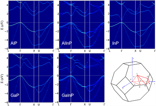
For GaP and AlP indirect bandgaps of about 2.3[ 22, 23 ] and 2.5 eV[ 24 ] were measured. In contrast, InP is a direct-gap semiconductor with a bandgap of 1.4 eV.[ 25 ] The direct–indirect bandgap crossover of Ga x In1−x P and Al y In1−y P occurs for In-poor and In-rich stoichiometries, respectively.[ 7, 26-28 ] The measured bandgaps of randomly ordering Ga0.5In0.5P and Al0.5In0.5P alloys amount to about 1.9[ 29, 30 ] and 2.3 eV.[ 31 ] In Figure 1 , we show the band structures of CuPt-type ordered GaInP and AlInP crystals, calculated at the respective equilibrium lattice constants of 5.71 and 5.70 Å obtained from structural relaxation. These lattice constants are nearly identical to the ones predicted by Vegard's law applied to the calculated lattice constants of the respective binary compounds[ 7 ] and about 0.7% larger than the experimental values.[ 32 ] Within GGA (HSE) we calculate direct and indirect band gaps of 0.57 (1.44) and 1.26 (2.06) eV for CuPt-type ordered GaInP and AlInP, respectively. Obviously, even the HSE values somewhat underestimate the experimental data.[ 29-31 ] This is largely due to ordering effects. In fact, the bandgap energy is expected to be highest in fully disordered alloys, with increased ordering leading to a bandgap decrease due primarily to a downward motion of the conduction band, as described by Wei and Zunger.[ 33 ] This effect is experimentally confirmed for GaInP[ 34 ] and AlInP.[ 35 ] The present calculations in comparison to earlier hybrid DFT calculations based on the same numerical parameters[ 7 ] indicate that ordering effects reduce the GaInP and AlInP bandgaps by 0.18 and 0.24 eV, respectively.
3.2 Natural Band Alignment
The HSE band structures calculated here can be used to determine the natural band alignment at GaInP/AlInP interfaces for CuPt-type ordered crystals within the branch-point method. We calculate valence and conduction band offsets of 0.14 and −0.54 eV, respectively. Compared with the HSE values calculated for random alloys,[ 7 ] the CuPt ordering of the bulk material is found to reduce the valence band offset by 0.04 eV and to increase the conduction band offset by 0.05 eV. This confirms earlier theoretical work[ 33 ] showing that ordering affects the conduction states more strongly than the valence states.
3.3 Interface Formation Energies
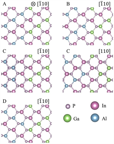
To go beyond the branch-point methodology, we next investigate four nonsymmetry-related possibilities to realize atomically smooth interfaces between CuPt-type ordered GaInP and AlInP, see Figure 2 . These are modeled here within periodic supercells, with lateral lattice constants corresponding to either GaInP or AlInP. This models the situation that either a thin AlInP film is grown on a GaInP substrate, or vice versa. Thus, both limiting interface realizations are included in the calculations. The supercell dimension along the interface normal, i.e., parallel to the [001] direction, is optimized to allow for vertical strain compensation.
| Interface | A | B | C | D | ||||
|---|---|---|---|---|---|---|---|---|
| Substrate | AlInP | GaInP | AlInP | GaInP | AlInP | GaInP | AlInP | GaInP |
| [eV atom−1] | 0.002 | 0.002 | −0.132 | −0.131 | −0.065 | −0.064 | −0.064 | −0.064 |
| [Å] | 5.71 | 5.70 | 5.69 | 5.68 | 5.70 | 5.69 | 5.70 | 5.69 |
| [eV] | 0.74 | 0.74 | 0.75 | 0.76 | 0.76 | 0.76 | 0.76 | 0.77 |
| [eV] | 0.03 | 0.03 | 0.04 | 0.05 | 0.05 | 0.05 | 0.05 | 0.06 |
3.4 Interface-dependent Band Alignments
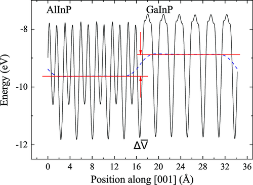
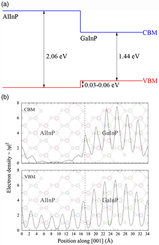
Here, is the difference between and the valence band edge calculated for bulk GaInP or AlInP within hybrid DFT and is the variation of across the interface, see Figure 3 . It is associated with the dipole that is set up across the interface and therefore a ground-state property, which is reliably calculated within DFT-GGA.[ 36 ] The values for and calculated here for the different interface configurations are summarized in Table 1. As can be seen from Figure 3, six layers are indeed sufficient for the planar averaged electrostatic potential to reach an almost constant value in both supercell regions. This indicates that sufficient material is included in the supercell for reliable calculations. The numerical error bars resulting from the averaging procedure are smaller than 20 meV. The differences in the valence band offsets calculated for thin GaInP films on AlInP substrates compared with the reverse situation are at most 10 meV, i.e., below the numerical error bar. This is due to the nearly perfect lattice match of the two ternary compounds. Also the spread of the valence band offsets calculated for the different microscopic interface realizations A to D is very small, only 30 meV. This indicates that the microscopic modeling of interface bonding, strain and dipoles is of minor importance for the band alignment at GaInP/AlInP interfaces. In fact, the microscopic modeling leads to a valence band offset that is at most 110 meV smaller than the value estimated from the branch-point method for ideally CuPt-type ordered crystals. Combining the calculated valence band offsets with the fundamental bandgaps calculated within hybrid DFT for AlInP and GaInP, 2.06 and 1.44 eV, respectively, provides the conduction band offsets. As summarized in Figure 4a, a type-I alignment is predicted here for the interface between CuPt-type ordered alloys, regardless of the actual interface configuration. Still, the valence band offsets calculated here are very small and have to be considered with some caution. Nevertheless, the present calculations agree with an earlier study[ 7 ] predicting a type-I alignment, albeit with a slightly larger valence band offset, between randomly ordered alloys.
3.5 Localized States
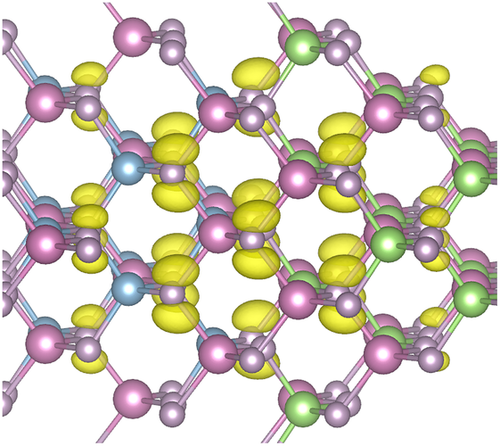
The type-I band alignment at the interface is also reflected in the spatial localization of the wave functions that form the valence band maximum und conduction band minimum of the superlattice structure used here for interface modeling. As shown in Figure 4b, both are localized in the GaInP region. As expected from the larger energy offset, the confinement of the conduction state is more pronounced than that of the valence state. Interestingly, bound interface states do not occur in the band gap region. However, at the point of the interface Brillouin zone, around 0.1–0.2 eV below the valence band maximum, bound interface-localized states exist. They correspond to phosphorous states with p character, as exemplarily shown in Figure 5 for the interface B. Specifically, the projection on atomic orbitals shows a contribution of and orbitals that amounts to more than .
4 Conclusion
In conclusion, (hybrid) DFT was used to characterize atomically smooth Ga0.5In0.5P/Al0.5In0.5P interfaces between CuPt-type ordered alloys. The interface, where the Ga(111) and In(111) plans of ordered GaInP alternate with In(111) and Al(111) planes of AlInP is most favorable. However, further interface structures occur within an energy range of less than 0.1 eV per interface atom and will therefore form as well. Irrespective of the ordering of the alloys and irrespective of the precise interface configuration, a type-I alignment of the band edges is found. The CuPt-type ordering of the alloys leads to a reduction in the valence band offset and an increase in the conduction band offset by 0.04 and 0.05 eV, respectively, compared with random alloy interfaces. For the interface between perfectly CuPt-ordered alloys, depending on strain and interface configuration, a valence band offset of 0.03–0.06 eV is predicted. There exist no interface states within the energy range of the fundamental gap. However, slightly below the valence band maximum interface-anion localized p states are detected. The microscopic interface calculations presented here suggest that predictions of the band alignment based on the branchpoint method are reliable within an error bar of 0.1 eV.
Acknowledgements
Financial support by DFG (PAK981, SCHM1361/26) is gratefully acknowledged. The authors thank the Paderborn Center for Parallel Computing (PC2) and the Höchstleistungs-Rechenzentrum Stuttgart (HLRS) for grants of high-performance computer time.
Open access funding enabled and organized by Projekt DEAL.
Conflict of Interest
The authors declare no conflict of interest.
Open Research
Data Availability Statement
The data that support the findings of this study are available from the corresponding author upon reasonable request.


