Highly Efficient and Broadband Achromatic Transmission Metasurface to Refract and Focus in Microwave Region
Abstract
Achromatic devices have wide application prospects in radar and imaging fields. However, chromatic aberration and limited bandwidth restrict their development. Moreover, broadband and highly efficient achromatic devices working in transmission mode are still difficult to realize. In this paper, broadband highly efficient achromatic transmission in the microwave region by a metasurface is achieved. First, the ideal dispersion conditions of achromatic meta-atoms are given. Then, a polarization selective grating metasurface and a split ring slot metasurface are designed using the transfer matrix method and equivalent circuit theory, respectively. The former is used to control phase characteristics while the latter enables controlling dispersion. Phase and dispersion can be controlled independently by cascading them and any phase curve can be designed as is desired. In order to verify the strategy, an achromatic deflector and an achromatic lens are designed and samples are fabricated. The experimental results show that the deflector can realize achromatic refraction from 9.3 to 12.3 GHz with average efficiency 77.5% and the lens can realize achromatic focusing from 9.8 to 12.2 GHz with average efficiency 78.9%, respectively. The experimental results are in good agreement with theory. The findings provide valuable strategy for achromatic devices design, which can be widely applied.
1 Introduction
In radar systems and imaging systems, chromatic aberration distorts the signal waveform caused by electromagnetic devices because the refractive index of electromagnetic materials varies with frequency.[1-5] With the rise of artificial metamaterials, researchers can design sub-wavelength unit cells and realize desired permeability and permittivity to modulate the wave front.[6-8]
In recent years, scientists have realized 2D planar electromagnetic devices, which are called metasurface,[9-35] such as, refraction devices,[36-40] meta-lenses,[41-51] and vortex generators.[52-56] In most of these devices, Lorentz resonance units are used.[57] Because of their strong resonance characteristic, their bandwidth is narrow. Therefore, electromagnetic devices exhibit different wave front modulation at different frequencies. For example, the refraction angle of a deflector changes with frequency, as shown in Figure 1a. In 2015, Cappaso first realized an achromatic lens with the same focal length at three frequencies experimentally.[58] Next, J. Yang realized a reflection achromatic focusing from 10.7 to 11.7 GHz.[59] However, achromatic focusing devices working in reflection mode limit application in imaging system. Later on, in 2018, J. Yang furtherly demonstrated a broadband achromatic lens from 7 to 9 GHz with average efficiency 54.6%.[60] In 2020, A. A. Fathnan realized achromatic Huygens’ metalenses from 8.5 to 9.5 GHz with efficiency above 70%.[61] The efficiency of transmission metasurface is lower than reflection mode because of large reflection and loss of materials. Therefore, it is important to realize highly efficient and broadband achromatic devices working in transmission mode.
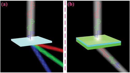
In this paper, first, we give dispersion conditions for achromatic meta-atoms according to theory.[61, 62] Next, we propose a novel strategy to achieve controlling phase and dispersion independently based on a polarization selective grating metasurface and a split ring slot metasurface, respectively. The cascade of two metasurface units can realize any required phase distribution and broadband high-efficiency transmission. In designing the two structures we use the transfer matrix method (TMM) and equivalent circuit theory, respectively. In order to verify our theory, we design a broadband deflector, which realizes achromatic refraction from 9.3 to 12.3 GHz experimentally (Figure 1b) with average efficiency 77.5%. Meanwhile, we also design a lens, which realizes achromatic focusing from 9.8 to 12.2 GHz with average efficiency 78.9%. Because the cascaded meta-atom also has the function of converting x-polarized wave to y-polarized wave, the output beam of both deflector and lens is in cross-polarization mode. Our findings pave the way for broadband high-efficiency transmission achromatic devices with potential applications in radar and microwave imaging systems.
2 Results and Discussion
2.1 Broadband Achromatic Deflector Design
2.1.1 Dispersion Conditions of Broadband Achromatic Refraction
2.2 Meta-Atom Design
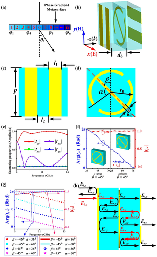
In order to realize broadband achromatic refraction, we have to design a meta-atom with broadband linear phase response and high transmission. Our design consists of three parts. First, we propose a meta-atom A, which consists of three layers with metal (yellow) as shown in Figure 2b. There are two parallel metal gratings with both pairs being orthogonal to each other. The middle layer contains a circular ring with diagonal metal bar structure. This meta-atom can realize broadband linear phase response and high transmission. In addition, it can induce an arbitrary phase change varying from 0 to 2π.[63, 64] Second, we design a meta-atom B which consists of a multi-layer split ring slot structure as shown in Figure 3a. This structure can also realize broadband linear phase response and high transmission. The difference with meta-atom A is that with meta-atom B arbitrary dispersion can be realized by changing the number of layers and the width of the slot. The physics mechanisms behind the phase delay of meta-atom A and meta-atom B are all based on the propagation phase principle.[65, 66] We finally cascade the two kinds of metasurface structures to obtain the desired phase change and dispersion property.
As shown in Figure 2b–d, in the first structure three layers with a metal structure are alternated by two dielectric layers (blue). The metal is made of copper with conductivity σ = 5.8×10⁷ S m−1 and thickness 0.036 mm. The substrate is made of FR-4 with relative permittivity of 4.3, a loss tangent of 0.025. To realize broadband highly efficient transmission and a phase change that depends linearly on the frequency, we choose the following initial values for the parameters shown in Figure 2b–d. The period p of meta-atom is 6 mm. The width l1, the thickness h0, and the length of metal gratings is 1.6, 0.036, and 6 mm, respectively. The distance l2 between metal gratings is 1.4 mm. The radius r0 and the width w0 of circular ring is 2.8 and 0.3 mm, respectively. α and β are 80° and 45°, respectively. The thickness d0 of substrate is 2 mm. The electromagnetic behavior of meta-atom A is characterized using CST Microwave Studio and the method can be seen in Section 4.
In order to understand this broadband highly efficient transmission structure, we utilize the TMM to explore the property of the meta-atom.[67] The TMM is applicable for a multi-layer structure. As illustrated in Figure 2h, when there is a y-polarized incident wave from the left it is almost totally reflected, whereas when a x-polarized wave is incident from the left, a y-polarized wave with large amplitude is transmitted into the right medium because of the process of repeating reflection and transmission inside the meta-atom. The specific analytical process can be seen in Part A, Supporting Information.
Next, we study the phase controlling properties. As shown in Figure 2f, the transmission phase is determined by α and the rotation angle (β) of middle layer circular ring structure. For the frequency 11 GHz, when β is 45° and α changes from 22° to 76°, the phase change is from 0 to π. When β is −45° (the circular ring structure turns 90° clockwise as shown in the left inset in Figure 2f and α changes from 20° to 74°, the meta-atom can induce a phase change between π and 2π. At the same time, the transmission efficiency is always over 0.9. In addition, we show in Figure 2g the frequency dependence for several choices for β and α. The phase curves show a linear dependence between frequencies 9 and 13 GHz as required and they are parallel to each other. The amplitude curves show that transmission rate is always over 0.9 over the entire band. As a result, changing α and rotation direction of the diameter bar inside the circular ring gives phase coverage from 0 to 2π without affecting the dispersion relation.[48]
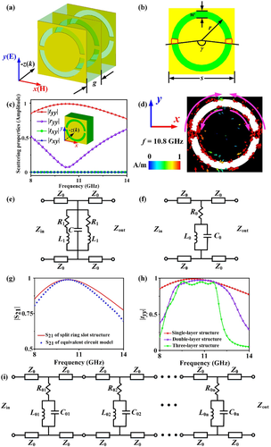
In the second step of the design process, we consider multi layers metal sheets with split ring slots (yellow part) separated by air gaps (green part) as shown in Figure 3a. The thickness of the air gap is ≈.[68] The metal is aluminum with conductivity σ = 3.5×10⁷ S m-1 and the thickness 0.2 mm. In order to support the metal sheet structures, the air gaps are filled with foam material with permittivity 1.15 and loss tangent 0.0057. The density is 110 kg m−3 and the compression strength is 2.9 MPa. Similarly, to obtain broadband high-efficiency transmission and a linear phase response, the parameters of meta-atom B are chosen as following. The period s of meta-atom B is 12 mm. The width w and the external radius r of the slot is 1.6 and 5.2 mm. is 170°. The thickness hm of the metal sheet is 0.2 mm. The thickness g of the foam is 6 mm. We mainly focus on this structure responding to y-polarized waves. The transmission and reflection of a single-layer structure is shown in Figure 3c, which is for a y-polarized wave incident normally and propagating in the negative z-direction. The amplitude of tyy is larger than 0.9 for frequencies from 9 to 13 GHz.
Here, we adopt equivalent circuit principle to explore the physical mechanism of the broadband high-efficiency transmission property.[69-72] First, we observe in Figure 3d the surface current distributions on the metal for the frequency 10.8 GHz where |tyy| is maximum. There are strong opposite resonant currents on both sides of the split ring slot, which are indicated by the pink arrows. In addition, strong currents also exist at the two gaps between the two semicircle slots indicated by the red circles in Figure 3b. We establish an equivalent circuit to analyze the electromagnetic characteristics of this structure, as shown in Figure 3e. The split ring slot is considered to be equivalent to a capacitance C; either of the two gaps indicated by the red circles is equivalent to be an inductor L1 and a resister R1 in series. These two equivalent circuits are parallel.
We simplify the equivalent circuit in Figure 3e to a LC parallel circuit, which is shown in Figure 3f. Thus, the single-layer split ring slot structure can be considered as a first-order band-pass filter, which could realize high-efficiency broadband transmission from 9 to 13 GHz. According to |tyy| in Figure 3c, we can derive the values of R0, L0, and C0 of the LC parallel circuit by utilizing circuit simulation software AWR Design Environment and find R0, L0, and C0 is 5.13×10⁻⁵ Ω, 110.37 nH, and 0.08064 pF. The resonant frequency ω0 derived from the circuit simulation software is 10.6 GHz. Then, we plot S21 of equivalent circuit calculated by AWR as shown in Figure 3g. It coincides well with S21 of physical model calculated by CST. The results above indicate the reliability of our equivalent circuit model theory. A multi-layer structure can be equivalent to a nth-order band-pass filt, which is shown in Figure 3i.[73] Furthermore, we study the relationship between the transmission bandwidth and the order of the filter, that is, the number of layers of the structure. The transmission property is shown in Figure 3h for different numbers of metal sheet layers with the same structural parameters. We find that the high-efficiency transmission bandwidth gradually narrows in agreement with theoretical predictions.[73] However, the three-layer structure still can realize high-efficiency transmission from 9 to 12 GHz.
Next, we consider the phase response of the split ring slot structure. In Figure 4a the phase of tyy is shown as function of frequency for several numbers of layers. A linear dependance of the phase on frequency is observed from 9.2 to 12.9 GHz, which we will call the linear region. When the number of layer increases, the slope of phase curves increases. We also consider the influence of the width w of the slot for the double-layer structure as a typical research. Figure 4b illustrates the variations in the amplitude and phase as function of frequency for several values of w. For smaller w the high-efficiency transmission band becomes narrower while the slope of the phase curves becomes larger. Single-layer and three-layer structures show similar properties. All phase curves show a linear dependance on frequency in the band from 9.3 to 12.6 GHz.
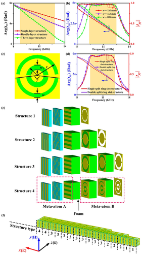
In order to increase the slope of the phase curves and reduce the thickness of this structure as much as possible, we propose a double split ring slot structure. The front view of the structure is shown in Figure 4c, where a second slot is added inside the original circular slot. The parameters of the added structure are w1 = 1.8 mm and r1 = 2.8 mm while the other parameters remain unchanged. We compare the transmission of the three-layer double split ring slot structure with the three-layer single split ring slot structure. The results are shown in Figure 4d. It is seen that by adding the slot, the slope of the phase curve increases while the bandwidth where the transmission is high remains. The linear region of the phase curves is from 9.5 to 12.3 GHz. Similarly, when we reduce the width w of the original slot, the slope of the phase curves increases while the bandwidth of high transmission gradually reduces. Thus, adding a slot is an effective way to widen the controlling range of dispersion property without increasing the thickness of the structure. In a word, we can carefully design meta-atom B to achieve dispersion relation of transmission as we desire.
In the third step of the design process, we cascade four meta-atom A with period of 6 mm placed 2 × 2 and one meta-atom B with period of 12 mm to form 4 types of meta-atom C with period of 12 mm. Meta-atom A and meta-atom B are separated by foam material (green part) with thickness of 6 mm. Every layer of the 4 structures is shown in Figure 4e. With these structures we can realize broadband high efficiency transmission with the slope of phase curves gradually increasing. At the same time, we can control the phase response and its slope independently by changing the circular ring with the metal diagonal bar structure and the width of split ring slot respectively. The cascaded meta-atom also has the cross-polarization conversion function.
2.3 High-Efficiency Broadband Transmission Achromatic Deflector Design and Experimental Verification
According to working frequency band of our meta-atoms, we design an achromatic refraction metasurface with phase difference between adjacent meta-atoms at 12 GHz. On the basis of theoretical Equation (1), it can be calculated that refraction angle θt is 20.3°. To have the angle of refraction constant for all frequencies in the band of interest, the difference of slope in phase curves induced upon transmission between adjacent meta-atoms should be Rad GHz−1.
To realize this phase relationship and dispersion property, we design a broadband achromatic refraction metasurface which contains 16 meta-atoms. All of the meta-atoms are composed of four types of structures as shown in Figure 4e. We design the structures by adjusting α and the rotation direction β of the circular ring with diagonal metal bar structure, and furthermore the outer slot radius r and width w of the metal sheet. Other parameters remain fixed as described mentioned above. We arrange 16 meta-atoms into 1D linear array, which is shown in Figure 4f with marked structure type of every meta-atom. Amplitude curves of them are shown in Figure S2, Supporting Information. Phase curves are shown in Figure 5a. The transmissivity of all meta-atoms is above 0.8 from 9.8 to 12.4 GHz. At the same time, all of phase curves show great linear characteristics from 9.6 to 12.5 GHz and the slope of curves increases evenly. In order to better assess the linearity of the phase response, we also give the spectral derivative of the phase profile in Figure S3, Supporting Information.[74]
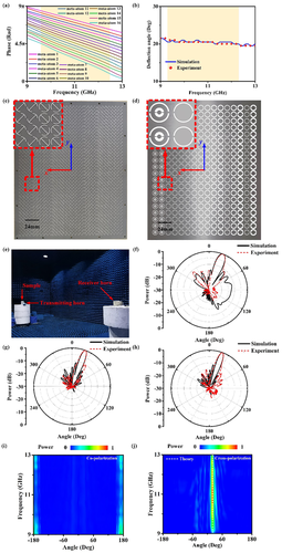
20 groups of 1D linear array are configured repeatedly along y-axis with a period of 12 mm and the whole area is 192×240 mm2. We carry out simulation of the model in CST Microwave Studio. X-polarized plane wave is incident along z-axis. We take the direction of maximum radiation energy as the deflection angle and observe y-polarized wave from 9 to 13 GHz. The deflection angle curve is in Figure 5b. From 9.2 to 12.3 GHz, the deflection angle is always between 20.0° and 21°, which is consistent with theoretical value, 20.3°. The slight deviation may result from phase error of elements and finite size of model.
To furtherly demonstrate our design theory and simulation, we fabricate a sample and the size is the same as simulation model (16 × 20 cells with a total size of 192 × 240 mm2). Two layers of sample are shown in Figure 5c,d and all of layers can be seen in Figure S4, Supporting Information. Then, we test far field characteristics of our sample in microwave anechoic, as shown in Figure 5e. The method can be seen in Section 4. The measurement results of deflection angle are shown in Figure 5b. The deflection angle is between 20.0° and 21.0° from 9.3 to 12.3 GHz, which is in good agreement with simulation results. Inevitable fabrication errors and imperfections of the incoming wave fronts generated by the microwave horn lead to tiny difference.
In order to analyze the effect of achromatic refraction, we give the simulation and experiment normalized far-field patterns at 9.3, 10.8, and 12.3 GHz in Figure 5f–h. We can find that the main lobe of the patterns refracts and the simulation (experiment) refraction angle is 20.5° (21.0°), 20.5° (20.5°), and 20.0° (20.0°) at 9.3, 10.8, and 12.3 GHz, respectively. The edge diffraction component of co-polarization in the normal direction hardly has effect on the observation of deflection component because we merely observe cross-polarization component. This contributes to high polarization purity of our device. The measured 2D scattering power spectrums varying against angle and frequency of co-polarization and cross-polarization are shown in Figure 5i,j. In the operation band, the power distribution concentration angle of cross-polarization is almost consistent with theoretical deflection angle. Instead, outside of operation band, most co-polarization power is reflected around normal direction.
Next, we calculate working efficiency of our device. The efficiency is defined as the ratio between the power of the main beam regions and the total power of the incident wave. As shown in Figure 6a, the experiment efficiency is in consistent with simulation result. The fluctucation of experiment results comes from noise random error, measurement error, and sample fabrication error. The efficiency of experiment is over 70% from 9.7 to 12.3 GHz. It reaches peak (86.7%) at 11.3 GHz. The average efficiency is 77.5%. The lost power mainly results from reflection, edge diffraction and the loss of substrate.
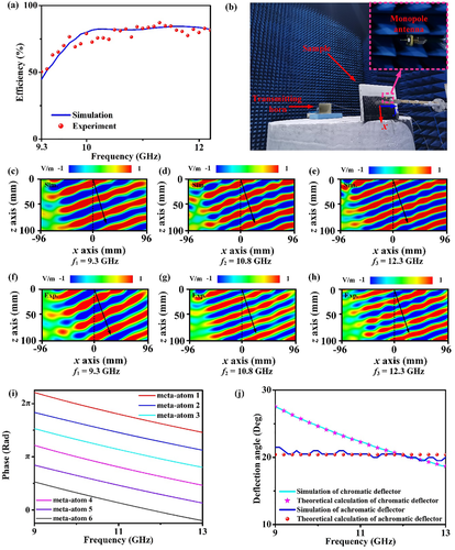
At last, we test the near-field characteristics of the device. The test schematic diagram is shown in Figure 6b. The method can be seen in Section 4. Figure 6f–h give the y-polarization electric field distributions at 9.3, 10.8, and 12.3 GHz. When the wave is incident on the metasurface, the propagation direction of electric field obviously refracts. The flat transmission wave front proves the high efficiency of the device. The experimental results are in good agreement with simulation results.
We also give a comparison between chromatic and achromatic deflector. We design a chromatic deflector with meta-atom A and optimize six meta-atoms with phase interval between adjacent meta-atoms. The phase curves of all meta-atoms are shown in Figure 6i. We can see that phase curves are parallel to each other. In another word, the phase interval is always among the whole band. In order to ensure the fairness of comparison, the period and the size of chromatic deflector is the same as achromatic deflector. Then, we plot deflection angle varying against frequency of chromatic deflector by conducting simulation (finite-different-time-domain method) in Figure 6j. It is obvious that the deflection angle decreases with frequency increasing. The simulation is in good agreement with theory. On the contrary, for our achromatic deflector, the deflection angle remains stable as we desire. This comparison furtherly proves the correctness of our achromatic deflector theory and design.
2.4 Application for Achromatic Focusing Lens
2.4.1 Dispersion Conditions of the Broadband Achromatic Focusing Lens
2.4.2 Broadband Achromatic 1D Lens Design and Experimental Verification
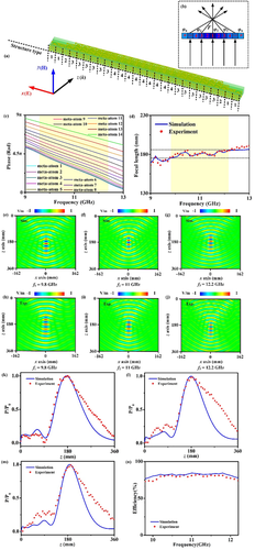
We design a 1D broadband achromatic lens with the focal length of 180 mm. According to Equation (3), we can obtain the phase and dispersion distribution of achromatic lens. Then, we design the achromatic lens consisting of 14 kinds of meta-atoms. Namely, n is 14 in Figure 7b. They are also composed of four types of structures in Figure 4e. Then, we arrange meta-atoms into 1D linear array along x axis to form 1D lens. The schematic diagram is shown in Figure 7a with marked structure type of all the meta-atoms. All of meta-atoms can realize over 80% transmission from 9.7 to 12.3 GHz, which ensures high-efficiency of the device. The transmittivity curves of 14 meta-atoms can be seen in Figure S5, Supporting Information. In Figure 7c, all of transmission phase curves show great linear property from 9.6 to 12.4 GHz.
25 groups 1D linear array are configured repeatedly along y-axis with a period of 12 mm and the area is 324×300 mm2. We carry out simulation with open boundary conditions in all directions. X-polarized plane wave is incident normally to the metasurface along z-axis. We simulate the energy distribution of array central axis along z direction and determine the focus at the point of maximum energy. The simulation focal length varying against frequency is shown in Figure 7d (marked with blue solid line). We take the error of 5 mm as acceptable error. We can find that the focal length is between 175 and 185 mm from 9.8 to 12.2 GHz.
In order to furtherly verify the performance of our lens, we also fabricate a lens sample and the size is the same as the simulation model (27 × 25 cells with a total size of 324 × 300 mm2). Next, we test the near-field property of our sample in microwave anechoic. From Figure 7h–j, we can find EM wave goes through metasurface and the focusing effect is obvious at 9.8, 11, and 12.2 GHz. The experimental results prove the accuracy of our meta-atom phase design. The experimental results are in good agreement with simulation results, which are shown in Figure 7e–g. We also extract the energy distribution (|Ey|2) along z-axis and find that the focal length of experiment is consistent with that of simulation among the whole band, which is shown in Figure 7d.
Then, we normalize the energy along array central axis in z direction and the distribution curves are shown in Figure 7k–m. The maximums of energy curves are all around 180 mm. The experimental results are in good agreement with simulation results. The differences between simulation and experiment result from imperfect incident wave front from the transmitting horn. They also come from sample fabrication error, measurement error and noise error. Next, we calculate the efficiency of achromatic lens. The computational process in detail can be seen in Part B, Supporting Information. Finally, we get the efficiency of experiment and simulation from 9.8 to 12.2 GHz, as shown in Figure 7n. The experimental efficiency is over 80% from 10.3 to 11.8 GHz and remains steady. It reaches peak (82.3%) at 11.2 GHz. The average efficiency is 78.9%. The results above indicate broadband achromatic focusing property of our device. We compare the performances of our work with the reported microwave achromatic lens in term of operation band, relative bandwidth as well as efficiency in Table 1. We can find that the efficiency of our design is better than other work.
3 Conclusion
In conclusion, we propose a novel strategy to realize high-efficiency broadband achromatic transmission based on metasurface. First, we give the dispersion conditions to be satisfied by achromatic devices. Then, we design the meta-atom which controls phase and dispersion independently based on polarization-selective grating metasurface and split ring slot metasurface. The design mechanisms are based on TMM and equivalent circuit theory. Next, we design an achromatic deflector and an achromatic lens. Finally, we fabricate samples and conduct experiments. The experimental result verifies the feasibility of our idea. Our design strategy enriches the research of metasurface and provides novel thought about achromatic device design. They will have potential applications in radar or imaging systems.
4 Experimental Section
Simulation and Numerical Methods
All of simulations are conducted in CST Microwave Studio. When the transmission amplitude and phase property of a meta-atom were studied, Frequency Domain Solver was used and periodic boundary conditions were applied around the meta-atom. Two Floquet ports were set 30 mm away from both surfaces of the meta-atom.
For the array simulation, Time-Domain Solver was used and open boundary conditions were applied in all directions of the array. The plane wave was always incident normally on the surface of the meta-atom or array.
Experimental Methods
Far field and near field experiments were all conducted in the microwave chamber. For the far field test of the deflector, as shown in Figure 5e, the sample was fixed in the center of the rotary table. The transmitting horn emitted plane wave which was perpendicular to the surface of the sample. The rotation of the rotary table was controlled and the transmittivity of different angles can be measured with a fixed receiver horn in far field. The transmitting and receiving horns were connected to the vector network analyzer Agilent so that the signals can be detected.
For the near field test of the deflector, as shown in Figure 6b, the sample was fixed on the edge of the platform. The transmitting horn was placed on one side of the sample and emitted plane wave which was perpendicular to the surface of the sample. Monopole antenna was used as a receiver to detect the distribution of y-polarization electric field on xoz plane on the other side. The near field test of the lens was analogous.
Acknowledgements
W.J. and T.C. contributed equally to this work. This work was supported by National Natural Science Foundation of China (Nos. 61871394, 61901512), Postdoctoral Innovation Talents Support Program of China (No. BX20190293), and Natural Science Foundation of Shaanxi province (No. 2019JQ-013).
Conflict of Interest
The authors declare no conflict of interest.
Open Research
Data Availability Statement
The data that support the findings of this study are available from the corresponding author upon reasonable request.


