Modulation of surface stiffness and cell patterning on polymer films using micropatterns
Abstract
Here, a new technology was developed to selectively produce areas of high and low surface Young's modulus on biomedical polymer films using micropatterns. First, an elastic polymer film was adhered to a striped micropattern to fabricate a micropattern-supported film. Next, the topography and Young's modulus of the film surface were mapped using atomic force microscopy. Contrasts between the concave and convex locations of the stripe pattern were obvious in the Young's modulus map, although the topographical map of the film surface appeared almost flat. The concave and convex locations of a polymer film supported by a different micropattern also contrasted clearly. The resulting Young's modulus map showed that the Young's modulus was higher at convex locations than at concave locations. Hence, regions of high and low stiffness can be locally generated based on the shape of the micropattern supporting the film. When cells were cultured on the micropattern-supported films, NIH3T3 fibroblasts preferentially accumulated in convex regions with high Young's moduli. These findings demonstrate that this new technology can regulate regions of high and low surface Young's modulus on a cellular scaffold with high planar resolution, as well as providing a method for directing cellular patterning. © 2017 The Authors. Journal of Biomedical Materials Research Part B: Applied Biomaterials published by Wiley Periodicals, Inc. J Biomed Mater Res Part B: Appl Biomater, 106B: 976–985, 2018.
INTRODUCTION
In recent years, technologies that regulate the stiffness of soft materials for use as cell culture scaffolds have attracted increasing attention. The migration,1-6 proliferation,7-11 differentiation,12-17 and metabolism10, 18-20 of mammalian cells can be controlled by modulating the surface stiffness of the cellular scaffold. Notably, cells have a tendency to migrate from surfaces with low Young's moduli to surfaces with high Young's moduli, thereby promoting the aggregation of cells into desired patterns by locally regulating the Young's modulus of the substrate.4, 21-27
Previous methods for the local regulation of the surface stiffness of cellular scaffolds include physical connection of substrates with differing Young's moduli, topological arrangement of scaffold regions using varying concentrations of a crosslinking agent,4, 21-26 and localized photo-crosslinking of scaffold regions.27-30 However, these methods are only applicable to crosslinkable polymers, and the generated chemical structure and surface topography are non-uniform between crosslinked regions and non-crosslinked regions.28 Various activities of mammalian cells are affected by these chemical31-33 and topographical discrepancies,18, 34-40 and, therefore, consideration must be given to the effects of surface parameters other than stiffness on cellular functions.
To preferentially alter surface stiffness alone, flat and homogeneous scaffold materials are ideal. Recently, a homogeneous polymer solution was applied to a micropattern, followed by regioselective adjustment of the Young's modulus to create a scaffold with the capacity to control cellular localization and arrangement.41 However, vertical intervals of >1 μm remained on the scaffold surface, and the overall Young's modulus showed gentle slope changes for several tens of micrometers.
The current study proposes an improved surface stiffness regulation method that can be applied not only to crosslinkable polymers but also to various non-crosslinkable biomedical polymers. This new technology could locally regulate regions of high and low surface Young's modulus while maintaining uniform chemical structure and surface topography, because homogenous films as flat as a spin coated film will be used for the method. Our novel method is aiming to generate local changes in surface Young's modulus by merely using a micropattern to support an elastic film. Importantly, cultured cells could be arranged in desired shapes on the surface of the newly fabricated cellular scaffold based on areas of varying stiffness.
MATERIALS AND METHODS
Cells, reagents, and experimental instruments
Round glass coverslips (diameter = 40 mm) were purchased from Matsunami Glass Ind., Ltd. (Osaka, Japan). Polyvinyl alcohol (PVA; MW = 25,000) was purchased from Polysciences, Inc. (Warrington, PA, USA). Poly(ε-caprolactone) (PCL; MW = 70,000–100,000) and chloroform (special grade) were purchased from Wako Pure Chemical Industries, Ltd. (Osaka, Japan). Sponge swabs were purchased from As One Corporation (Osaka, Japan). Vaseline® petroleum jelly was purchased from Yakuhan Pharmaceutical Co., Ltd. (Shizuoka, Japan), and washers (PCW-1022–02; outside diameter = 22 mm, inside diameter = 10.5 mm, thickness = 2 mm) were purchased from Hirosugi-Keiki Co., Ltd. (Kanagawa, Japan). VECTASHIELD® mounting medium was obtained from Vector Laboratories (Burlingame, CA, USA), and EUKITT® mounting medium was purchased from O. Kindler GmbH & Co. (Freiburg, Germany). Glass bottom dishes (50 × 7 mm, aperture = 40 mm) were obtained from WillCo Wells B.V. (Amsterdam, the Netherlands), and Kimwipes were purchased from Nippon article Crecia Co., Ltd. (Tokyo, Japan). Nail varnish was used common goods which is clear and colorless.
NIH3T3 cells were obtained from DS Pharma Biomedical Co., Ltd. (Osaka, Japan). Dulbecco's Modified Eagle's Medium (DMEM; D6046, low-glucose), penicillin-streptomycin solution (P4333), 0.25% trypsin-EDTA solution (T4049), a PKH26 red fluorescent cell linker kit (PKH26GL), and TWEEN® 20 (P1379) were purchased from Sigma-Aldrich (St. Louis, MO, USA). Fetal bovine serum (FBS; Gibco 26140) and Alexa Fluor 488-phalloidin (A-12379) were obtained from Invitrogen (Carlsbad, CA, USA). Phosphate-buffered saline (PBS, pH 7.4) containing 4% paraformaldehyde was purchased from Nacalai Tesque, Inc. (Kyoto, Japan). DAPI was purchased from Dojindo Laboratories (Kumamoto, Japan). Cell culture dishes (100 × 20 mm) were purchased from Corning (Tewsbury, MA, USA). All water used in this study was Milli-Q water.
Fabrication of micropatterns
Cell culture scaffolds consisted of a flat, elastic PCL layer (see below) adhered to a micropattern. The micropatterns were fabricated on a square silicon substrate (725 μm thick, 10 × 10 mm) by photolithography.39, 40 Deep etching of the silicon substrate was performed using the Bosch process for deep reactive ion etching. Patterns were generated in nine regions (2 × 2 mm) of the substrate, and each patterned area was 500 μm from the adjacent patterned areas. Photolithography was performed using a photomask. Although nine patterns were drawn in the photomask, only the six patterns described below are discussed in this study. Thirty-nine parallel rectangular slits (25 μm wide, 2 mm long, spaced 25 μm apart), 51 parallel rectangular slits (25 μm wide, 2 mm long, spaced 12.5 μm apart), 61 parallel rectangular slits (25 μm wide, 2 mm long, spaced 6.25 μm apart), 25,281 light-shielding squares [10 µm on one side, spaced at intervals of 2.5 µm and aligned in a grid shape (159 × 159 columns)], 17,689 light-shielding squares [10 µm on one side, spaced at intervals of 5.0 µm and aligned in a grid shape (133 × 133 columns)], and 12,996 light-shielding squares [10 µm on one side, spaced at intervals of 7.5 µm and aligned in a grid shape (114 × 114 columns)] were drawn onto the photomask in the six regions.
Micropattern shapes were observed and analyzed via color laser three-dimensional (3 D) microscopy with a VK-9700 instrument (Keyence Co., Osaka, Japan). To analyze the shapes of the patterns, areas (704.5 × 528.4 μm) were imaged using a 20 × 0.46 numerical aperture (NA) objective (Nikon Co., Tokyo, Japan). The overall view of the silicon substrate with its nine component patterned regions was imaged using a Power Shot SX210 IS digital camera (Canon, Inc., Tokyo, Japan).
Fabrication of the PCL film as an elastic layer
After dust was removed from a round glass coverslip with a stream of nitrogen gas, the coverslip was spin-coated (4000 rpm, 50 sec) with an aqueous solution of PVA (70.6 g/l). Next, the PVA-coated coverslip was further spin-coated (4000 rpm, 50 sec) with a PCL (13.7 g/l) chloroform solution to generate an elastic PCL film. PVA formed a releasable layer between the PCL film and the coverslip. The thickness of the PVA/PCL two-layer film was analyzed by color laser 3 D microscopy with a VK-9700 instrument and a 150 × 0.95 NA objective (Nikon Co.).
Adherence of the PCL film to the micropatterns
The procedure used to adhere the PCL film to the micropatterns is described in Figure 1. First, a 1 cm-square micropatterned substrate was adhered and secured by nail varnish to the center of a round glass coverslip (Figure 1a). Next, a sponge cotton swab and a Pasteur pipette were used to surround the area around the substrate with Vaseline® in a circular shape, and the Vaseline® was spread outward in a radial fashion. An appropriate amount of EUKITT® was then dripped between the radial “arms” of the Vaseline®. Before the EUKITT® could dry, a coverslip with a PCL film was adhered from above, with the PCL film surface facing downward (Figure 1b). To increase adhesiveness, a weight was placed directly on top of the micropatterned substrate, and the unit was left standing overnight (Figure 1c). Throughout the preceding steps, the micropatterned substrate with a concavo-convex pattern was sandwiched between two glass coverslips (Figure 1d). After the EUKITT® dried, the sandwiched micropatterned substrate was inserted into a 100 mm dish and immersed overnight in degassed water. One of the two coverslips was removed by dissolving the PVA, leaving only the PCL film on the concavo-convex micropatterned substrate. After removal of the coverslip, the inside of the dish was drained. A Kimwipe was used to lightly remove the water droplets, and the unit was allowed to dry. Next, an appropriate amount of VECTASHIELD® mounting medium was spread on one surface of a washer, and the washer was placed on the substrate such that the hole of the washer was aligned with the center of the substrate (Figure 1e). Finally, a weight was placed on the washer and left overnight. This protected the PCL film adhered to the concavo-convex micropattern and improved substrate adhesiveness and flatness (Figure 1f). The thickness of the PCL film was analyzed by color laser 3 D microscopy using a VK-9700 instrument. The substrate was imaged from the surface of the PCL film to the surface of the micropattern using a 150 × 0.95 NA objective.
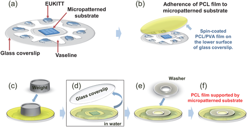
Fabrication of PCL film supported by a micropattern. (a) A 1 cm-square micropatterned substrate was adhered and secured by nail varnish to the center of a round glass coverslip. (b) A coverslip with a PCL film was adhered from above, with the PCL film surface facing downward. (c) To increase adhesiveness, a weight was placed directly on top of the micropatterned substrate, and the unit was left standing overnight. (d) After the EUKITT® dried, the sandwichedmicropatterned substrate was immersed overnight in degassed water. One of the two coverslips was removed by dissolving the PVA, leaving only the PCL film on the concavo-convex micropatterned substrate. (e) The washer was placed on the substrate such that the hole of the washer was aligned with the center of the substrate. (f) This protected the PCL film adhered to the concavo-convex micropattern and improved substrate adhesiveness and flatness.
Generation of topology and Young's modulus maps
Topology and Young's modulus maps of the micropattern-adhered PCL film were generated by atomic force microscopy (AFM) in AM-FM viscoelastic mapping mode.42 The mapping setup is shown in Figure 2. The AFM analysis employed a MFP-3 D-BIO instrument (ASYLUM RESEARCH an Oxford Instruments company, Santa Barbara, CA, USA) and an AC-240-R3 rectangular cantilever AFM probe (Olympus Optical Co., Ltd., Tokyo, Japan) operated at a spring constant of 1.71 N/m and a resonant frequency of 70 kHz.
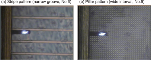
Mapping of the topographies and Young's moduli of the PCL film surfaces. AFM was used to map the topography and Young's modulus of the PCL film surface adhered to each micropattern. (a) Mapping of the PCL film adhered to the number 6 narrow-groove stripe pattern. (b) Mapping of the PCL film adhered to the number 9 wide-interval pillar pattern. In both cases, the patterns under the PCL films can be seen due to the transparent nature of the film.
The Young's modulus maps were converted from the AM-FM viscoelastic maps by applying 406 MPa to the Young's modulus of the micropattern-adhered PCL film at the convex location, because the surface Young's modulus of the PCL film attached to a flat silicon substrate was measured at 406 ± 43 MPa (n = 5) using AFM. This value of the measured Young's modulus of the PCL film agrees with that in other reports.43-46
Cell culture on micropatterned cellular scaffolds
The PCL film attached to the micropatterned silicon wafer was placed into a 100 × 20 mm cell culture dish and sterilized under ultraviolet irradiation for 15 min. Next, the micropattern-adhered PCL film was immersed overnight in degassed sterile water and then washed three times with degassed medium consisting of DMEM, 10% FBS, and 1% penicillin-streptomycin. NIH3T3 cells were seeded onto the film at a density of 1 × 10⁴ cells/cm2 and cultured for 24 h at 37°C with 5% CO2. The cells were then fixed with PBS containing 4% paraformaldehyde and stained with Alexa Fluor 488-phalloidin (1:250, 6 h) and DAPI (1:2000, 20 min) to label F-actin and the nuclei, respectively.
Fluorescence images of the stained cells and reflection images of the micropattern-supported PCL film were simultaneously captured via confocal laser scanning microscopy with a FV-1000 D instrument (Olympus Optical Co., Ltd., Tokyo, Japan), a 20 × 0.75 NA objective (Olympus), and an image scan area of X = 634.6 μm, Y = 634.6 μm, and Z = 200 μm. To obtain images that included the cells, the PCL film, and the micropattern, imaging was performed at 0.5 µm intervals from the upper surface of the cells to a depth of 200 µm in the Z direction.
Statistics
Statistical analyses were performed using GraphPad Prism software (GraphPad Software, Inc., La Jolla, CA, USA). Quantifiable data are presented as the mean ± standard deviation. An unpaired t test with Welch's post-hoc correction was used to compare pattern shape values with Young's modulus image values. In all cases, P values of < 0.05 were considered significant (n.s., not significant; *, p < 0.05; **, p < 0.01; and ***, p < 0.001).
RESULTS
First, nine different micropatterns were simultaneously fabricated on a 1 cm-square silicon wafer by photolithography. The overall view of the silicon wafer was imaged using a digital camera. As shown in Figure 3a, the area of each coexisting pattern was approximately the same, measuring ∼2 × 2 mm. Of the nine fabricated micropatterns (numbered 1 to 9), this study focuses on pattern numbers 4 through 9. The shapes of these six patterns were assessed, and the results are shown in Figure 3b-g. These micropattern shapes both the top view and the side view were observed and analyzed via color laser three-dimensional (3 D) microscopy. Average values and standard deviations were determined based on six different measurements using an analysis software attached to the color laser 3 D microscopy. Pattern number 4 exhibited a wide-groove stripe pattern consisting of 24.6 µm-wide grooves at 24.8 µm intervals (Figure 3b), while pattern number 5 exhibited a middling groove stripe pattern consisting of 12.7 µm grooves of moderate width spaced at 24.5 µm intervals (Figure 3c), and pattern number 6 exhibited a narrow-groove stripe pattern consisting of 5.8 µm narrow grooves at 25.0 µm intervals (Figure 3d). Pattern number 7 consisted of pillars with a square-shaped top pillar surface of 9.9 µm on one side and pillars spaced at narrow 2.5 µm intervals and aligned in a grid shape (Figure 3e), while pattern number 8 consisted of pillars with a square-shaped top pillar surface of 8.8 µm on one side and pillars spaced at moderate 6.6 µm intervals and aligned in a grid shape (Figure 3f), and pattern number 9 consisted of pillars with a square-shaped top pillar surface of 8.2 µm on one side and pillars spaced at wide 9.1 µm intervals and aligned in a grid shape (Figure 3g). The depth (height) of each pattern was nearly equivalent, at ∼26–31 µm (Figure 3b-g).
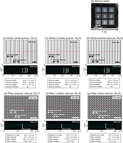
Evaluation of micropattern shapes. (a) A 1 cm-square silicon wafer containing nine types of micropatterns (numbered 1 to 9) is shown. (b) Top and side views of the number 4 wide-groove stripe pattern. (c) Top and side views of the number 5 middlegroove stripe pattern. (d) Top and side views of the number 6 narrow-groove stripe pattern. (e) Top and side views of the number 7 narrow-interval pillar pattern. (f) Top and side views of the number 8 middleinterval pillar pattern. (g) Top and side views of the number 9 wide-interval pillar pattern. The side views provide cross-sectional images of the micropattern areas indicated by red lines in each of the top views. Average values and standard deviations were determined based on six different measurements. Scale bars in (b)-(g): 50 μm.
Next, a two-layer PVA/PCL elastic film for adherence to the micropatterns was fabricated by spin coating the polymers onto a round glass coverslip. The PVA layer dissolved easily in water and was used as a releasable layer between the PCL film and the coverslip. The thickness of the two-layer film was 56.5 ± 0.6 µm (n = 5 measurements using VK-9700). The film was attached to the micropatterns to form a cellular scaffold, and care was taken to ensure that the film did not peel away from the micropattern or warp in the cell culture medium. The fabrication procedure is described in Figure 1. Figure 4a shows the PCL film adhered to the silicon wafer after dissolution and release of the PVA layer from the coverslip in water. The thickness of the adherent PCL film was 50.2 ± 2.5 µm (n = 5 measurements using VK-9700). Consequently, PCL cellular scaffolds with a thickness of ∼50 µm were obtained that contained the above-described stripe and pillar patterns (Figure 4b).
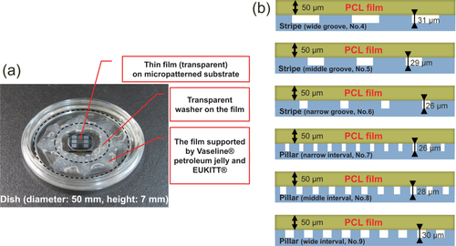
Overview of micropatterned cellular scaffolds comprising a PCL film. (a) Overview of cellular scaffolds comprising a PCL film adhered to a silicon wafer containing micropatterns. (b) Illustrated cross-sections of six types of cellular scaffolds.
Topographical and Young's modulus maps of the scaffold surfaces were attained via AM-FM viscoelastic mapping mode AFM. A PCL film containing the narrow-groove stripe pattern is shown in Figure 5a-c, and a PCL film containing the pillar pattern is shown in Figure 5d-f. Although the films appeared nearly flat in the topographical maps, areas of clear contrast were apparent in the Young's modulus maps. For example, the dark areas in Figure 5a-c corresponded to the grooves of the stripe pattern, while the bright areas in Figure 5d-f corresponded to the pillars of the pillar pattern. In both cases, the bright and dark areas in the Young's modulus maps represent convex and concave areas of the patterns, respectively. Moreover, these areas were clearly demarcated on any micropattern-containing PCL films.
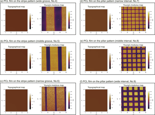
Topographical and Young's modulus maps of cellular scaffold surfaces observed by AFM. (a)-(c) Topographical and Young's modulus maps of cellular scaffolds consisting of PCL films adhered to stripe patterns with wide, middle, and narrow grooves, respectively. (d)-(f) Topographical and Young's modulus maps of cellular scaffolds consisting of PCL films adhered to pillar patterns with narrow, middle, and wide intervals, respectively. Details of the topographical maps of the cellular scaffolds are shown in Supplementary Figure S1.
The dark areas had a low Young's modulus in the Young's modulus maps, while the bright areas had a high Young's modulus. Based on the maps obtained, the Young's moduli of the film areas supported by the convex pattern regions were clearly higher than those of the concave regions. Thus, film stiffness can be locally regulated by the shape of the micropattern supporting the film. Incidentally, the topographical map of the elastic films shows an almost flat surface, but there is a slight deflection toward the grooves or pillar bases at concave regions. The greatest distance the elastic film deflected toward the base was 53 nm, which was observed for pattern number 4, the wide groove stripe pattern. This distance is so small as to be insignificant compared with the size parameters of the micropattern (for example, groove width, groove interval, and groove depth), the film thickness, and the cell size. Figure S1 details the topographical map and the deflection distance of the elastic film on each micropattern.
Next, we addressed the positional accuracy with which the Young's modulus of the film surface can be regulated. The Young's modulus maps of Figure 5 were analyzed to determine the groove width, groove interval, length of one side of the top surface of the square pillars, and spacing between the square pillars. These data were compared with the values obtained for the patterns shown in Figure 3. Table 1 shows that, for both the stripe patterns and the pillar patterns, the average values for groove width, groove interval, length of one side of the top pillar surface, and spacing between square pillars deviated very little between the pattern shape image and the Young's modulus image.
| Stripe (wide groove, No.4) | Stripe (middle groove, No.5) | Stripe (narrow groove, No.6) | ||||
|---|---|---|---|---|---|---|
| Shape image | Young's modulus image | Shape image | Young's modulus image | Shape image | Young's modulus image | |
| Groove width [µm] | 24.6 ± 0.1 | 24.8 ± 0.2 | 12.7 ± 0.2 | 13.2 ± 0.1 | 5.8 ± 0.2 | 6.3 ± 0.2 |
| Groove interval [µm] | 24.8 ± 0.4 | 26.3 ± 0.5 | 24.5 ± 0.2 | 25.2 ± 0.2 | 25.0 ± 0.3 | 25.6 ± 0.2 |
| Number of samples (n) = 6 | ||||||
| Pillar (narrow interval, No.7) | Pillar (middle interval, No.8) | Pillar (wide interval, No.9) | ||||
| Shape image | Young's modulus image | Shape image | Young's modulus image | Shape image | Young's modulus image | |
| Square on a side [µm] | 9.9 ± 0.2 | 10.2 ± 0.2 | 8.8 ± 0.1 | 10.3 ± 0.3 | 8.2 ± 0.2 | 10.3 ± 0.1 |
| Pillar interval [µm] | 2.5 ± 0.3 | 2.6 ± 0.2 | 6.6 ± 0.2 | 5.2 ± 0.1 | 9.1 ± 0.2 | 7.6 ± 0.2 |
| Number of samples (n) = 6 | ||||||
Then, we cultured NIH3T3 cells on micropattern-containing PCL films. NIH3T3 cells cultured on a PCL film supported by the number 4 wide-groove stripe pattern were imaged using confocal laser microscopy. Figure 6 shows that 10 of the 12 cells scanned were present at locations supported by convex regions of the stripe pattern, particularly at the boundaries between the convex and concave regions. The two cells present at concave regions were also in contact with the boundary. Cells on PCL films supported by the other two stripe patterns or any of the pillar patterns were not imaged because the positions of the patterns could not be confirmed on the reflected image.
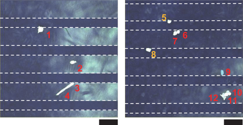
Cell culture on the PCL film supported by a micropattern. Two fluorescence confocal microscopy images of NIH3T3 cells cultured for 24 h on a PCL film supported by the number 4 wide-groove stripe pattern are shown. The fluorescence images of F-actin and DAPI-stained cellular nuclei were superimposed on the reflected image of the stripe pattern. The images were captured from the level of the upper scaffold surface to a depth of 200 μm at 0.5 μm intervals. The cells numbered in red are localized to the convex regions of the pattern, and the cells numbered in yellow are localized to the concave regions. Scale bars: 100 μm.
DISCUSSION
The data in Table 1 were used to generate graphs to compare the shape image value and Young's modulus value of each micropattern size parameter. The graph for the stripe patterns is shown in Figure 7a, while the graph for the pillar patterns is shown in Figure 7b. As shown in Figure 7a and b, there was not a large difference between the values of the shape image and the Young's modulus image for each micropattern size parameter. The largest difference for the stripe patterns was 0.5 μm which is 8.6% of the shape image of groove width of pattern number 6, the narrow-groove stripe pattern. The largest difference for the pillar patterns was 2.1 μm, which is 25.6% of the shape image of the length of one side of the top surface of the square pillars of pattern number 9, the wide-interval pillar pattern. Subsequently, no significant difference was observed between the values of the shape image and the Young's modulus image for the width of the grooves of the number 4 wide-groove stripe pattern or for the interval of the square pillars of the number 7 narrow-interval stripe pattern. Both of the micropatterns that have no significant difference in each size parameter are considered to be able to control the local surface stiffness with higher precision.
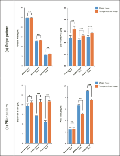
Comparison of shape image and Young's modulus image values of the stripe (no. 4–6) and pillar patterns (no. 7–9). (a) The groove width and interval of the stripe pattern are plotted along with the groove width and interval measured from the Young's modulus image of the film adhered to the stripe patterns (no. 4–6). (b) The length of one side of the square pillar component and the interval between the square pillars are plotted along with the length of one side of the square pillar component and the interval between the square pillarsmeasured from the Young's modulus image of the film adhered to the pillar patterns (no. 7–9). n.s., not significant; *, p < 0.05; **, p < 0.01; and ***, p < 0.001
The Young's modulus image versus the shape image of convex regions supporting the film tended to show a larger size, except for the number 7 narrow-interval micropattern, which had no significant differences. The differences between the Young's modulus image and shape image values are hypothetically attributable to the thickness of the film. If the film thickness were decreased, it is possible that the difference between the shape image and the Young's modulus image of the pattern would disappear.
With the above results, we demonstrated that a micropattern can be employed to accurately create a film surface with areas of high and low Young's modulus on the micrometer scale. The ability to regulate stiffness with this high level of spatial precision regardless of the film thickness (here, ∼50 μm) is extremely interesting. Our future plans include the fabrication of scaffolds with films of various thicknesses supported by micropatterns and the mapping of the Young's modulus of the generated scaffold surfaces. We will then estimate the influence of film thickness on spatial precision in Young's modulus regulation.
Figure 6 shows that NIH3T3 cells cultured on the PCL film preferentially accumulated at locations supported by convex regions of the stripe pattern, particularly at the boundaries between the convex and concave regions. This type of cellular localization is thought to result from the cells seeking adequate surface stiffness and then aggregating at an area with a high Young's modulus.4, 21-30
The current research introduces a new technology that can not only precisely regulate areas with varying surface Young's modulus on a cellular scaffold but also direct cellular arrangements for particular applications (that is, to create tissue-mimetic cellular patterns). By using this technology, we anticipate that areas with high and low Young's moduli can be produced on the surfaces of all types of elastic films by merely adhering the film to a micropattern with a 3 D shape. By controlling the thickness of the film, fine adjustments to the Young's modulus are likely possible.
One of our forthcoming goals is to develop a method to easily peel away an elastic film after adherence to a micropattern by using a temperature-responsive polymer. Such an accomplishment would yield a reusable 3 D template for controlling surface stiffness, in turn allowing the high-volume production of “cellular sheets” on which cells are arranged in a desired form. Because stiffness can be modified without altering the chemical composition/structure or topography of the sheets, this technology is practical and has a broad range of commercial and scientific/biomedical/tissue engineering applications.
In the field of regenerative medicine, the safety and affinity of cellular scaffolds within living organisms are high priorities. Therefore, the ability to immediately apply the present technology to existing biocompatible polymer materials is a major selling point. Our future endeavors will include the development of cellular sheets for regenerative medicine, in which cellular patterning appropriate for the replacement of lost tissue is strictly controlled.
CONCLUSIONS
Thus far, regulation of the local stiffness of cellular scaffold surfaces on the micrometer scale has been performed by changing the chemical composition or chemical structure of particular regions within the substrate surface. By contrast, our newly introduced technology can selectively produce areas of high and low Young's modulus without changing the homogenous chemical composition or chemical structure of the starting material. This new technology generates a cellular scaffold by adhering an elastic PCL film onto a micropattern, significantly altering the film stiffness at convex and concave locations of the micropattern. Furthermore, cells can be successfully arranged with positional selectivity at areas supported by convex regions of the micropatterns, which exhibit higher stiffness. Our future work will demonstrate regulation of areas with varying surface Young's modulus on various cellular scaffolds by using 3 D micropatterns, promoting cellular patterning for many applications. Unique features of this methodology include not only precision positional selectivity but also the ability to apply the practice to numerous different elastic films.
ACKNOWLEDGMENTS
This work was supported by JST PRESTO “Nanosystems and Emergent Functions,” a MEXT Grant-in-Aid for Young Scientists (A) (20680024), MEXT Grants-in-Aid for Exploratory Research (21657037, 25560186, and 15K14493), and a MEXT Grant-in-Aid for Scientific Research (B) (15H03008). The microfabrication of scaffolds in this study was supported by Hokkaido Innovation through Nanotechnology Support (HINTS) centered at Hokkaido University and Nano-Integration Foundry (NIMS) Nanofabrication Platform of the “Nanotechnology Platform Project” operated by MEXT, Japan. AM-FM viscoelastic mapping mode AFM measurement was supported by ASYLUM RESEARCH, an Oxford Instruments company.


