The role of oxygen vacancies in the high cycling endurance and quantum conductance in BiVO4-based resistive switching memory
Funding information: Fundamental Research Fund for Centre University; National Natural Science Foundation of China, Grant/Award Numbers: 11874003, 11904015, 51472016, 51672018; Natural Science Foundation of Beijing Municipality, Grant/Award Number: Z180007
Abstract
Resistive random access memory (RRAM) has emerged as a new discipline promoting the development of new materials and devices toward a broad range of electronic and energy applications. Here, we realized a memristive device with weak dependence on the top electrodes and demonstrated the quantized conductance (QC) nature in BiVO4 matrix. The electronic properties have been investigated by the measurements of I-V curves, where the resistive switching (RS) phenomenon with stable switching ratio and excellent long-term retention capabilities are identified. Two more inert materials, TiN and Pd, are applied as the top electrodes to exclude the influence of electrodes on the RS states and QC behavior. The X-ray photoelectron spectroscopy results and transport measurements reveal that the conductive filament (CF) is composed by elemental bismuth. The naturally existed oxygen vacancies in BiVO4 matrix plays as the role of catalyst in the formation and dissolution of CF in BiVO4-based RRAM device, which is the primary cause for the observed weak dependence of switching performance in this device on the type of top electrodes. Our results clearly illustrate that BiVO4 could be a new idea platform to realize the high scalability, high cycling endurance, and multilevel storage RRAM devices.
1 INTRODUCTION
As one of the most promising candidates for the next-generation memory, resistive random access memory (RRAM) has been studied intensively due to its outstanding properties compatible to current semiconducting industry, such as high scalability, low fabrication cost, simple sandwiched structure, long-term retention of state, high cycling endurance, and multilevel storage.1-5 In principle, RRAM is a phenomenon of resistive switching (RS) and made up by two parts, that is, SET and RESET. The step of SET corresponds to a transition from a resistance state (HRS) to a low resistance state (LRS) by forming the conductive filaments (CFs), where the HRS and LRS are responsible for the logic “0” and “1” states in binary memory, respectively. The step of RESET is correlated to the transition from LRS to HRS by the rupture of the conductive channels. Thus, the formation and rupture of CF are the key factors in the determination of performance of RRAM. In fact, RRAM can be classified into two main types, electrochemical metallization (ECM) and valence change mechanism (VCM), based on different forming mechanisms of CF. The CF in ECM device is constituted by the metal from top active electrodes with low standard electrode potential (SEP) and high standard Gibbs formation energy, such as Ag and Cu electrodes.6-9 The electrodes are initially oxidized to be anions under a positive voltage, and then the anions are driven through the insulating layer to the bottom electrode by the electric field, in which the anions are reduced into metal filament when the energy is higher than its standard redox potential. The high standard Gibbs formation energy resists the anions to be captured by ions during the transmission process, which significantly enhances the formation efficiency of CF. Furthermore, the low SEP promise the low SET and RESET voltage, benefiting to promoting its potential application in low power operation. Nevertheless, the high motilities of these noble metals in dielectric layer could evoke the spontaneous filament decay, which is detrimental to the retention capabilities of ECM devices. In contrast, VCM devices express the long-term retention of state because the CF is derived from the dielectric materials with oxygen vacancies induced by the migration of oxygen ions to react with top electrode.1, 10 In this case, the top electrode performs as the oxygen ions reservoir during the SET and RESET process. Therefore, RS ratio shows a strong dependence on the standard Gibbs formation energy of top electrodes and its value could vary in a huge range even in the same dielectric material.11 Looking for the appropriate dielectric materials in VCM devices with the features independent of the electrode types is highly desired. The oxygen vacancies naturally present in some bismuth oxides, such as α-Bi2O3 and BiMnO6, and Bi nanowires could be formed after applying the electric field, making bismuth oxides be the good candidates for RRAM regardless of the effect of electrodes.12, 13 In addition, the quantum conductance (QC) behavior, which plays a crucial role in the application of multilevel ultrahigh-density storage, could be realized in the metal nanowires in the condition that the lateral dimension of the nanowires is comparable to the Femi wavelength of conduction electron.14-16 However, the main mechanism dominating the QC levels is still unclear. Further work toward controlling the QC values is strongly demanded before the potential applications.
In our work, the RRAM device with the simple sandwich structure Ti/BiVO4/F-doped tin-oxide glass (FTO) has been successfully fabricated by the hydrothermal method. The electronic properties have been investigated by the measurements of I-V curves, where the RS phenomenon with stable switching ratio and excellent long-term retention capabilities are identified. Two more inert materials, TiN and Pd, are applied as the top electrodes to exclude the influence of electrodes on the RS states and QC behavior. The X-ray photoelectron spectroscopy (XPS) results and electronic resistivity vs temperature (R-T) curves are also measured, demonstrating that the composition of CF is Bi nanowires. Moreover, the lateral radii of the Bi channels at different conductance levels have been calculated according to the Schrödinger's equation for a cylindrical CF structure. Finally, the single cylindrical CF mode is established based on our results and analysis, indicating that BiVO4 could be an idea candidate for nanoelectronics.
2 RESULTS AND DISCUSSION
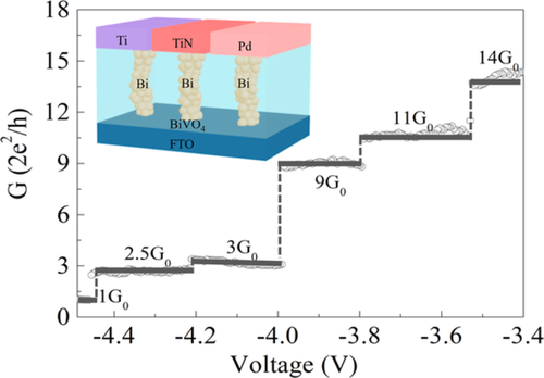
The monoclinic scheelite BiVO4, which has been studied intensively as photoanode in solar water splitting due to that its energy bandgap (2.4 eV) could adsorb substantial portion of the visible spectrum, was adopted as the medium material in our RRAM device.17, 18 Typical polyhedron structure of BiVO4 is displayed in Figure 1A, where the structural unit cell is constructed by VO4 tetrahedron and BiO8 dodecahedron.19 X-ray diffraction measurement in Figure S1 shows a well-developed single phase and can be indexed as polyhedron structure, verifying its good crystallization in BiVO4 film. The Ti electrodes were deposited by magnetron sputtering on the surface of BiVO4 with help of specific mask to synthesis the two-terminal devices. Figure 1B displays the schematic of Ti/BiVO4/FTO structure in our RRAM devices, which is plotted based on the transmission electron microscopy results combined with energy dispersion spectrum in Figure S2. The RS from HRS to LRS is initially performed under a large positive voltage, as shown in Figure S3, which is termed as forming progress. After that, the SET of the device could be obtained at the low bias voltage (~3 V), and the RESET occurs at about −2 V with a confined current ICC = 5 mA to protect the device from broken. The device exhibited typical bipolar RS phenomenon with a hysteresis loop characteristic of memristive switching, as illustrated in Figure 1C. In contrast to the sharp transition in SET process, multiple current jumps were observed during the negative bias voltage sweeping progress. A representative plot of the conductance as a function of the bias voltage during the RESET process is deduced from the I-V curve (inset of Figure 1D) with the bias voltage ranging from −3.4 to −4.5 V, as shown in Figure 1D, where the QC steps with integral values are identified. The formation mechanism of QC will be discussed in detail below.

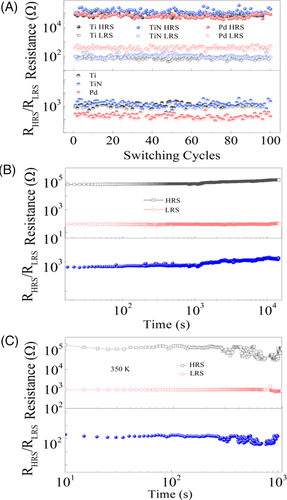
It is noticeable that there are several essential factors to evaluate the practical prospect of RRAM, such as on/off ratio, endurable ability, retention capability, and properties at high temperature. Figure 2A displays the resistance of LRS (RLRS) and HRS (RHRS) as a function of switching cycles in three kinds of device, Ti/BiVO4/FTO, TiN/ BiVO4/FTO, and Pd/ BiVO4/FTO. In the Ti/BiVO4/FTO, the RLRS (RHRS) is about 102 Ω (105 Ω) measured under the bias voltage of 0.5 V (−0.5 V) after the SET (RESET) progress. The switching ratio calculated by the ratio of RHRS to RLRS are all around 103 in the three devices, which is much larger than the critical value of on/off ratio in application of computer memorizer (~10).5, 20 Interestingly, RHRS, RLRS, endurable ability, and switching ratio retain the same values after replacing top Ti electrodes by TiN and Pd electrodes, the same measurement were carried as in the Ti/BiVO4/FTO device. It is well known that the performance of RRAM synthesized by both the ECM and VCM methods strongly depend on the top electrodes types.17 For example, the HRS value measured with the Ti top electrodes (~104 Ω) deviates obviously from that obtained with Pt top electrodes (~107 Ω) on the surface of TiO2 dielectric layer.11 The BiVO4-based devices perform the similar features of switching states regardless of the different standard Gibbs formation energies of top electrodes. In addition, Figure 2B displays that both the HRS and LRS are steady going over 4 × 10⁴ seconds at room temperature, demonstrating the high retention capabilities in this device. The good retention capabilities and cycling endurance, as shown in Figures 2C and S5, respectively, could also be identified at 350 K, which is the typical operational temperature for semiconductor device. Furthermore, Figure S6 implies the weak relationship between surface size of top electrodes and HRS (LRS), illustrating the CF growth mode is independently of the Schottky barrier on the Ti/BiVO4 junction. The existence of nanoscale filaments in the BiVO4/FTO structure has been confirmed by the conductive atomic force microscopy (C-AFM) images in the Figure S7. After applying a bias voltage of 5 V, massive conductive spots appear in the current map, indicating that the device is switched from HRS to LRS.

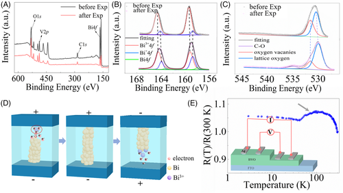
It is crucial to figure out the principle mechanism of formation and dissolution of the CF before the potential application of the RRAM devices. Thus, we performed the XPS measurements to make a comparative investigation of the chemical bonding in BiVO4 sample before and after CF forming process, as shown in Figure 3A. The fitting results of pristine BiVO4 sample in Figure 3B make it clear that there are two groups of bonding components in Bi 4f signals, labeled as Bi1 and Bi2, respectively. The energy gap of the two peaks in each group is a constant value, indicating that the two fitting peaks in one group are related to two Bi 4f5/4 and 4f7/4 peaks, respectively. The Bi 4f7/4 spectrum appears as two peaks, 159.5 and 158.7 eV, which are close to the bond values of Bi3+ and Bi+, respectively.21 It should be noted that valence state of Bi in pure BiVO4 sample is +3. The observation of the Bi+ signal is correlated to the natural oxygen vacancy in this system. After applying the voltage to form the CF in the BiVO4 matrix, the Bi 4f peaks are slightly redshifted compared with the value in pristine sample. The fitting results show that one more group of bonding components labeled as Bi3 could be identified in addition to the peaks contributed by Bi3+ and Bi+. The two low binding energy peaks in B3 group are centered at 163.0 and 157.7 eV, respectively, in accordance with the element Bi peaks reported previously.22 Therefore, the conductive CF is most probably composed by elemental bismuth. The peak intensity ratio between B2 and B1 is increased in BiVO4 matrix with CF compared to that in pristine BiVO4 sample, indicating that the Bi3+ anions are initially reduced to Bi+ and then to elemental Bi. For the O 1s signals, there are two peaks, marked with O1 and O2, in the pristine BiVO4 sample centered in the 531.6 and 530.5 eV, respectively, as shown in Figure 3C, indicating that there are two types of oxygen atom with different chemical environments. As the binding energies of the O 1s peaks for O2− and oxygen vacancy (Ov) are located at 530.4 and 531.5 eV, respectively, O1 (O2) are attributed to signals from O2− (Ov). The fitted XPS results of CF-formed BiVO4 matrix imply that the peak intensity ratio between O2 and O1 becomes small, demonstrating that the amount of Ov is decreased after the formation of CF.23 One satellite peak at 535.1 eV is correlated to the CO bond, which is induced by the contamination during the forming process.24 Based on the analysis of the fitted XPS results, it is inferred that the formation of elemental Bi CF is accompanied with the declined amount of Ov. Thus, the formation and dissolution mechanism of CF could be described as below: first, natural oxygen vacancies are driven by the electric field through the Coulomb force to the bottom electrodes, where the bismuth is with the high concentration and low valence state compared to the Bi3+ in idea BiVO4 matrix. The Bi3+ and/or Bi+ anions in the BiVO4/FTO interface are reduced to metallic bismuth when the bias voltage is gradually increased up to a critical value. Meanwhile, the oxygen ions in the high oxygen vacancies concentration area are expected to permeate into and to incorporate with local oxygen vacancies in other spaces to make the constant number of electrons in this system. In this case, the number of oxygen vacancies bonded with bismuth is decreased, consistent with the declined peak intensity of Ov after the formation of CF in BiVO4 film, as shown in Figure 3C. The device switches from HRS state to LRS state till the conductive channel (Bi) connects the top and bottom electrodes. Finally, when the polarity of the applied voltage is reversed, opposite electrochemical reactions take place on the BiVO4/FTO interface, where the elemental Bi reacts with the oxygen ions to form the Bi3+ (Bi+) ions and oxygen vacancies, dissolving the Bi CF from the bottom electrodes and resetting the system into HRS state. The schematic of the SET and RESET processes in BiVO4 matrix are plotted in Figure 3D. The dynamics of formation CF from bottom electrodes to top electrodes could be confirmed by XPS results of Bi 4f signals as a function of depth from the top surface, as shown in Figure S8, where the concentration of elemental Bi beneath are much higher than that in the top surface in the BiVO4 film after forming process.

The transport measurements of BiVO4 sample with CF at the temperature ranging from 2 to 300 K are performed to investigate the electronic properties of the formed CF. The schematic diagram is displayed in Figure 3E, where the one side of the BiVO4 matrix is thinned to promise that the charge carriers transport along the direction of CF perpendicular to the BiVO4 surface. An obvious arc between 50 and 300 K is observed in the curve, which is identified as the typical characteristic of the semimetallic Bi nanowires.25-27 The transport measurements confirm the formation of Bi CF we proposed in Figure 3D.
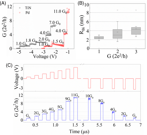
If the lateral dimension of the CF is comparable to Fermi wavelength of the dielectric material, the number of discrete sub-bands available for the electron transport becomes finite. Furthermore, each sub-band available for transport in the one-dimensional (1D) channel will contribute a conductance unit of G0 = 2e2/h, where e is electron charge, and h is Planck's constant.28, 29 The discrete change in the cell resistance with the integral units of the QC G0 can be clearly observed in Figure 1D, indicating a QC behavior. In order to figure out the distribution of the values of conductance steps, the statistical analysis of the conductance values from more than 1000 I-V curves during the RESET progress are counted and plotted in the histogram in Figure S9, where conductance concentrates at half-integer multiples value of G0. This half-integer quantized behavior could be attributed to a finite Fermi level split between top and bottom electrodes, leading to the diverse numbers of sub-bands available in the CF for the current injection from the top electrodes to bottom contacts.7, 30-33 The Landauer theory describes the conductance with the formula: G = T(2e2/h), where T is the transmits probability produced by obstacles in the channel. Thus, the fractional QC may result from the adsorbed impurities on or in atom chains, which changes the constriction configuration and affects the electronic band structure.34
 (1)
(1)
Here, μ is the effective electron mass of CF, and  is the nth zero of Bessel function to the lth order. Table 1 shows the calculated results of the CF radius in RRAM devices with different top electrodes initial quantized levels. The mean value of the radius of CF under different top electrodes is almost in the same range of 0.9 to 1.9 nm, demonstrating the weak relationship with top electrodes, as shown in Figure 4B. Furthermore, the radius of Bi filament is increased with the increment of the conductance, consistent with the theoretical predictions in the single filament model with the conductance less than 4 G0. The single filament model is confirmed by the results of measured conductance under the pulsed electronic filed with time width around several hundreds of nanoseconds. As shown in Figure 4C, the conductance value is enhanced step by step after applying a gradually growing pulsed voltage ranging from 0.5 to 3.5 V every 0.3 μs plus with the width of 0.1 μs. Moreover, conductance could be varied even after using the same value pulsed voltage, indicating that varied conductance is induced by different radius of Bi filament instead of other factors, such as the lifted Fermi surface induced different occupied sub-bands.28, 34, 35 The QC occurred not only in the RESET progress but also in the SET progress, demonstrating that BiVO4 is a reliable material as a memristor with multilevel storage applications.
| Ti/BiVO4/FTO | TiN/BiVO4/FTO | Pd/BiVO4/FTO | |
|---|---|---|---|
| 4 G0 (nm) | 1.376-1.256 | 1.158-1.124 | 1.538-1.206 |
| 2 G0 (nm) | 1.946-1.312 | 1.501-0.973 | 1.838-1.451 |
| 1.5 G0 (nm) | 1.451-0.988 | 1.376-0.988 | 1.226-0.937 |
| 1 G0 (nm) | 1.467-1.088 | 1.206-1.088 | 1.124-1.026 |
- Abbreviation: FTO, F-doped tin-oxide glass.
3 CONCLUSION
In summary, we realized a memristive device with weak dependence on the top electrodes and demonstrated the QC nature in BiVO4 matrix. The XPS results and transport measurements reveal that the CF is composed by elemental bismuth. The naturally existed oxygen vacancies in BiVO4 matrix plays as the role of catalyst in the formation and dissolution of CF in BiVO4-based RRAM device, which is the primary cause for the observed weak dependence of switching performance in this device on the type of top electrodes. Based on the single filament model, the sub-band spacing and Bi filament radius in BiVO4 are estimated. Our results clearly illustrate that BiVO4 could be a new idea platform to realize the high scalability, high cycling endurance, and multilevel storage RRAM devices.
ACKNOWLEDGMENTS
This research was funded by National Natural Science Foundation of China Grant/Award Numbers: 11874003, 51672018, 51472016, and 11904015; Beijing Natural Science Foundation Grant/Award Number: Z180007; and Fundamental Research Fund for Centre University. This wok was partially supported by UOW-BUAA Joint Research Centre.
CONFLICT OF INTEREST
The authors declare no conflict of interest.


