Principles, fabrication, and applications of halide perovskites-based memristors
Xiaozhe Cheng, Zhitao Dou, and Hong Lian contributed equally to this work.
Abstract
In recent decades, the microelectronics industry has developed rapidly based on the von Neumann architecture and under the guidance of Moore's law. However, as the size of electronic devices approaches the limit and power consumption increases, traditional microelectronic materials and devices are facing more and more challenges. As a new type of semiconductor material, halide perovskites (HPs) have excellent photoelectric characteristics, such as high carrier mobility, controllable band structure, etc., which have been widely used in solar cells, light emitting diodes (LEDs), photodetectors, memristors, and in other fields. Among them, the memristor, as a new type of electronic device, is very promising for in-memory computing with low power consumption by breaking the limit of von Neumann architecture. Especially, HPs-based memristors show outstanding photoelectric response performance, low power consumption, and flexible wearability, allowing them to hold great application potential in logical operation, polymorphic storage, and neuromorphic computing, etc. In this review, we first briefly introduce the basic characteristics and preparation methods of HPs. Secondly, the development history, device structure, and performance parameters of memristors are depicted in detail. Thirdly, the resistance mechanism and application of HPs-based memristors are discussed. Finally, the research status and development prospects of HPs-based memristors are outlined.
1 INTRODUCTION
With the rapid development of artificial intelligence (AI) and big data technology, the demand for high-calculus chips has become increasingly urgent in facing the trend of chip applications in diversified scenarios. However, on the one hand, due to the limit of memory and computation separation problems in the traditional von Neumann architecture, the chip memory speed is much slower than that of the processor (i.e., the “memory wall”).1, 2 At the same time, when large amounts of data are repeatedly exchanged between the memory and processor, the power consumption is strictly limited by computer cooling standards (i.e., the “power consumption wall”).2 On the other hand, the increasingly severe short-channel effects in the device lead to the fact that the gate cannot precisely control the ON/OFF states of the transistors. As a result, chip performance can no longer be improved by reducing device size (Moore's law slows down or even fails).3, 4 Therefore, the development of new materials and devices with in-memory computing and ultra-low power consumption abilities can further improve the performance of computing devices from the underlying design and expand the scale of computing capabilities.
As a new type of passive circuit component, memristor is regarded as an in-memory computing device that can break through the von Neumann architecture and maintain the effectiveness of Moore's law. It is known that the memristor is able to change its resistance state by applying an external current or voltage. According to the way the resistance changes, it can be divided into digital type (also called mutant type) and analogy type (also called slow type).5-8 Digital memristors are suitable for fast operation and high-density information storage because their high-resistance states (HRSs) and low-resistance states (LRSs) can represent “0” and “1”. Based on the three working modes of R-R (resistance-resistance), V-R (voltage-resistance), and V-V (voltage-voltage), the digital memristor can complete Boolean operation. An analog memristor is suitable for continuously processing and changing electrical signals, which can complete multiplication and accumulation operations based on Ohm's law and Kirchhoff's law to construct neuromorphic networks. Memristors are highly similar to neural synapses when used in artificial neuromorphic computing. Structurally, the top electrode (TE), active layer, and bottom electrode (BE) of the two-terminal (2T) structured memristor correspond to the presynaptic membrane, synaptic cleft, and postsynaptic membrane of the synapse, respectively.9, 10 Functionally, the antilog memristor can change the synaptic weight by changing the resistance value to achieve short-term plasticity (STP) (including paired-pulse facilitation (PPF), paired pulse depression (PPD), etc.), long-term plasticity (LTP) (including long-term potentiation (LTP) and long-term depression (LTD)),11-13 and brain-like learning and memory functions based on Hebbian learning laws such as spike-time-dependent plasticity (STDP).14 Therefore, memristors with the feature of integrating memory and computing have potential applications in AI, neural networks, and big data, etc.
Currently, resistive properties have been found in both inorganic and organic materials such as metal oxides,15 two-dimensional (2D) materials,16 polymers,17 natural proteins,18 small molecules, and perovskites, etc.19 Inorganic material-based memristors typically exhibit stable resistive behaviors, but normally are obtained with complex fabrication processes and high power consumption. Organic material-based memristors usually have the advantages of flexibility and low cost, but poor stability and short life. HPs, as a type of perovskite material, have flexible components that can combine the advantages of organic and inorganic materials, showing excellent properties such as a narrow band gap (1.2–2.5 eV), a high optical absorption coefficient, and a long carrier diffusion length.9, 10, 20 The earliest discovery of HPs can be traced back to the report by H. L. Wells in 1893,21 and have now been widely used in solar cells,22 LEDs,23 photodetectors,24 lasers,25 memristors,26 and in other fields. In the study of HPs-based solar cells, it was discovered and confirmed that the current hysteresis effect due to halogen ion migration is a resistive property, which opened a new door for the study of HPs-based memristors.27 With high ion migration rates and low defect migration barriers, HPs-based memristors have shown great potential for applications in information storage and artificial synapses.28
2 FUNDAMENTAL KNOWLEDGE OF HPs
2.1 Crystal structures of HPs
The general chemical formula for HPs is ABX3, where A = methylammonium (MA+), formamidinium (FA+), and Cs+, etc., B = Pb2+, Ge2+, and Sn2+, etc., and X = Cl−, Br−, and I−, etc. The ideal crystal structure of HPs belongs to the Pm3m cube space group (Figure 1A).29 The positive ion A with a certain radius occupies the center of the cube, and the positive ion B and the six anions X occupy the central site and six corners of the octahedron, respectively, which are located at the vertex of the cube.30 However, the actual crystal lattice will be distorted due to the different atomic radii of the components, resulting in reduced symmetry.29 Besides, when the cations of B are partially or fully vacant or replaced by other cations with different valences, perovskites with stoichiometry different from ABX3 will be obtained, such as A2BCX6, A2B(I)B(III)X6, A3BX6, A2B(V)X6, and A3B2(V)X9 (Figure 1B–F). Among the above crystal perovskites, ABX3, A2B(I)B(III)X6, and A3B2X9 are often used in the study of memristors, and the corresponding representative compounds are MAPbI3, MA3AgBiI9, and Cs3Bi2I9.
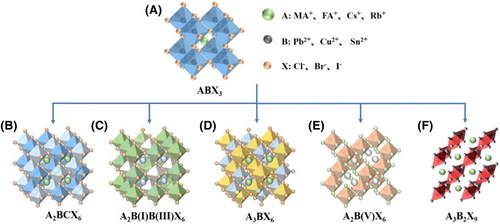
Overview of the crystal structures of different HPs. (A) Ideal crystal structure of perovskites. (B) A2BCX6, B-site cation is partially replaced by another metal ion C(II) (such as Sn2+). (C) A2B(I)B(III)X6, B-site cations are replaced by B(I) and B(III) metal ions (such as Ag+ and Bi3+). (D) A3BX6, B-site cations are replaced by B(III) metal ions. (E) A2B(V)X6, B-site cations are replaced by B(IV) metal ions and vacancies. (F) A3B2X, B-site cations are replaced by B(III) metal ions and vacancies.
2.1.1 Classification of HPs
HP materials can be classified in different ways. According to the types of A-position elements, HPs can be divided into all-inorganic HPs, all-organic HPs, and hybrid organic–inorganic HPs. All-inorganic HPs means that the A, B, and X positions are all inorganic components, such as CsPbI3. Although all-organic HPs have been successfully prepared for the first time in 2018, they have not yet been studied in the field of memristors.31 Hybrid organic–inorganic HPs refer to those perovskites with A-position elements replaced by organic cations, such as MAPbI3. However, under the premise of ensuring the stoichiometric ratio, the components of each position in the cubic crystal structure of HPs can be composed of two or more kinds of ions, such as MAPbI3-xBrx and FA1-xMAxPbI3, etc. Generally, all-inorganic HPs have good environmental stability, but their synthesis temperature is high. The hybrid organic–inorganic HPs are easy to be synthesized by the solution method at low cost and have thus been widely applied in optoelectronic devices.
HPs can also be classified as lead-containing and lead-free HPs according to whether they contain lead elements or not. Lead-containing HP memristors usually show outstanding advantages such as low operating voltage, high switching ratio, low power consumption, and multi-level resistance characteristics. In addition, due to the low-temperature manufacturing process of lead-containing HP films, flexible HP memristors with stable performance in the bending state have been developed. However, the lead element is easy to combine with water vapor in the air which accelerates the degradation process of the device, and most importantly, the problem of lead toxicity significantly hinders their practical application.32 Thus, researchers have tried to partially or completely replace Pb2+ by other metal elements, such as Sn2+, Ge2+, Bi3+ and Sb3+, etc. Among them, Sn2+ and Pb2+ belong to the same main group, but Sn2+ is easily oxidized to Sn4+ in air due to the low standard redox potential.33 The substitution of Pb2+ with heterovalent ions, such as Bi3+ and Sb3+, typically leads to the formation of a low-dimensional structure instead of resulting in the oxidation of perovskites. Nonetheless, this substitution may lead to a certain extent of reduction in the photoelectric conversion efficiency.
From the microscopic scale of the crystal structure, HPs can be divided into three-dimensional (3D), 2D, one-dimensional (1D), and zero-dimensional (0D) HPs (Figure 2A–D).29 3D HPs are the most common species in the study of solar cells due to their intact and continuous crystal structure and high carrier mobility. 2D HP nanosheets can be obtained by thinning 3D HPs, which are more stable due to the lower formation energy.34 In addition, the charge carriers can be confined to move in the plane of 2D HPs, which is beneficial for decreasing the Vth and power consumption of 2D HP-based memristors. 1D HPs include HP nanowires (NWs) and HP nanorods (NRs) with high crystalline mass, a large surface volume ratio, and anisotropic geometry. Therefore, they normally show low defect state density, low carrier recombination, and long charge carrier lifetime, exhibiting strong light scattering and trapping effects and fast charge transport capability.35-37 0D HPs include HP nanocrystals (NCs) and HP quantum dots (QDs). The size of NCs is larger than the Bohr radius of exciton, so there is little trap-induced recombination of electrons and holes at surface traps.38 The radius of QDs is less than or close to the Bohr radius, and its defects are mainly located on the surface, so QDs have a high light responsiveness.39
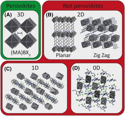
Crystal structure of hybrid organic–inorganic HPs with different dimensions. (A) 3D structure, where A is a small organic methylammonium cation. (B) 2D structure consisting of planar or zigzag angle-shared octahedra. (C) 1D structure consisting of octahedral chains shared by faces or corners. (D) 0D structure consisting of isolated metal halide octahedra. Reproduced with permission.29 Copyright 2020, American Chemical Society.
2.1.2 Preparation of HPs
Preparation of 3D HPs
As the most common perovskite species, the preparation methods for 3D HPs are quite mature, generally including the traditional solution method, spin coating method, and chemical vapor deposition (CVD) method. The traditional solution method is mainly used for the growth of perovskite single crystals, which is divided into solution temperature-lowering (STL),40 anti-temperature crystallization (ATC),41 and anti-solvent vapor-assisted crystallization (AVC).42 The STL method refers to the growth of perovskite crystals from a supersaturated solution by reducing the temperature. Although the method is simple and applicable, the growth period is relatively long, about 2–4 weeks to grow 1 cm.43 The ATC method is suitable for perovskite materials whose solubility decreases with the increase in temperature in some specific solvents, and the perovskite crystals prepared by this method can grow rapidly. Saidaminov et al. used the ATC method to grow 5 mm of MAPbI3 in just 3 h.41 The AVC method is used for the preparation of perovskite crystals through the different solubility of perovskite materials in different solvents. Tidhar et al. first proposed the concept of the ATC method in 2014.44 Then, in 2015, Shi et al. first obtained high-quality MAPbX3 in millimeter scale by the AVC method.42 The spin coating method is the most suitable method for preparing polycrystalline films in the laboratory at very low cost, which is mainly divided into one-step and two-step methods (Figure 3A,B).45, 46 During the spin coating process, the solvent evaporated, and the growth of the crystal underwent three processes: solution supersaturation, nucleation and growth.47-49 The one-step method refers to dissolving AX and BX2 precursors together in hybrid solvents to form a solution, which is then spin-coated onto the substrate and annealed to obtain polycrystalline film.50 The two-step method involves dissolving BX2 in a solvent first, then adding AX solution dropwise during the spin coating process of BX2 solution or directly immersing the spin-coated BX2 thin film into AX solution to obtain a high-quality perovskite film. For the first time, Mitzi et al. proposed a two-step method in which the PbI2 film was immersed in MAI solution, and the crystallization process can be completed through the interaction between organic and inorganic components.51 The CVD method is used to deposit perovskite film on substrates by thermal evaporation of AX and BX2 precursors under controlled conditions to give rise to a high-quality perovskite film. Liu et al. reported a dual-source co-evaporation of CH3NH3I and PbCl2 to obtain a perovskite film with high purity and excellent uniform thickness (Figure 3C). It can be seen from the scanning electron microscopy (SEM) image that the perovskite film prepared by the CVD method is more uniform and compact than that prepared by the solution method (Figure 3D,E).52
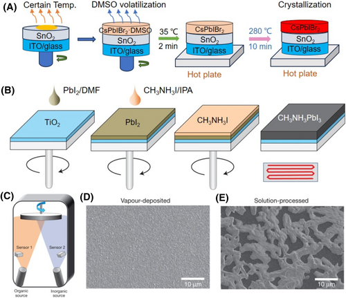
Schematic diagram of the preparation method of 3D HPs. (A) One-step spin coating method. Reproduced with permission.45 Copyright 2019, The Royal Society of Chemistry. (B) Two-step spinning method. Reproduced with permission.38 Copyright 2014, Nature. (C) CVD method. SEM top view of a vapor-deposited perovskite film. SEM top views of a vapor-deposited perovskite film (D) and a solution-processed perovskite film (E). Reproduced with permission.52 Copyright 2013, Nature.
Preparation of 2D HPs
2D HPs can be prepared by the solution method, the ligand-assisted reprecipitation (LARP) method, and the CVD method. The solution method can generate 2D HP nanosheets by evaporation or anti-solvent treatment of the precursor solution. Ni et al. obtained a uniform and dense MA3Sb2Cl9 film by dropwise addition of anti-solvent toluene when spin coating the precursor solution.53 The LARP method can effectively control the shape of the material with high repeatability, but ligands and surfactants may often contaminate the surface of 2D HPs. Sun et al. reported the synthesis of square and large-sized highly crystallized CsPbBr3 nanosheets with the assistance of oleic acid and octylamine.54 CVD method can precisely control the thickness and uniformity of 2D HPs. Ha et al. prepared 2D HPs with transverse dimensions of 5–30 μm and thicknesses ranging from a few atomic layers to several nanometers for the first time by using CVD method. The lead halide (PbX2, X = Cl−, Br−, I− or mixed halide) nanoplates were grown first on a muscovite substrate by van der Waals epitaxial technology in a gas phase transport chemical deposition system, and then the methylammonium halide molecules were inserted into the above PbX2 nanoplates to form MAPbX3 nanosheets by gas–solid isotropic reaction.55 In addition, it has been reported that 2D Cs3Bi2I6Cl3 can be synthesized by a stoichiometric melting reaction of CsCl and BiI3 at 750°C.56
Preparation of 1D HPs
The synthesis methods of 1D HPs include the gas phase synthesis method, the solution method, and the template method. The vapor phase synthesis method refers to the gas phase growth of HPs on the substrate by evaporating the precursors, resulting in 1D HPs with high crystal quality and low defect density. Figure 4A,B show the schematic diagram and the corresponding SEM image of CsSnX3 NWs prepared by Chen et al., using the gas phase synthesis method, respectively.57 The solution method shows great advantage in adjusting the morphology simply by changing the chemical reactants, and has high repeatability.58 The preparation of HP nanowires by the template method can be achieved by using inkjet printing equipment to directly inject perovskite ink into the nanopores of template, allowing the HP nanowires to grow in situ by further thermal annealing treatment. Lin et al. prepared highly ordered perovskite NWs by incorporating inkjet printing and an anodic aluminum oxide (AAO) confinement strategy as shown in Figure 4C.59 Figure 4D,E show the SEM image of the cross section of the prepared perovskite NWs and the schematic diagram of the perovskite NWs array inside the AAO nanopore, respectively. The HP nanowires prepared by the template method are of high quality and have a controllable morphology, but his method is relatively expensive and technically complicated.
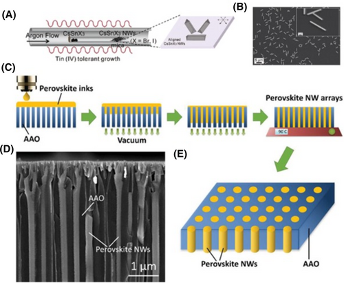
Schematic diagram of the preparation method of 1D HPs. (A) Schematic diagram of the device used to grow CsSnX3 nanorods by gas phase synthesis. (B) SEM image of the short CsSnBr3 wires grown for 20 min. Inset shows a zoomed-in SEM image of the CsSnBr3 wires. Reproduced with permission.57 Copyright 2009, American Chemical Society. (C) Fabrication and morphology of inkjet printed perovskite NW arrays. (D) Cross-sectional SEM observation of the perovskite NWs within the AAO nanostructure. (E). Schematics of perovskite NW arrays within the AAO nanopores. Reproduced with permission.58 Copyright 2020, Willey-VCH.
Preparation of 0D HPs
The methods for the synthesis of 0D HPs or HP QDs mainly include LARP method,60 thermal injection method,61 and template method.62 HP QDs can be prepared by LARP method because HP compounds have different solubility in different solvents. By changing surface ligands and precursors, the size, morphology and composition of HP QDs can be easily controlled (Figure 5A).63 In 2004, Schmidt et al. synthesized MAPbBr3 QDs with an average size of 6 nm for the first time by LARP method.64 The thermal injection method can be used to prepare colloidal HP QDs with an average size of 4–15 nm by adjusting the reaction time, solution concentration, and other parameters (Figure 5B).65 The template method is to spin coat the precursor solution onto a mesoporous template (such as SiO2 66 nanocrystalline films), and then the growth of HP nanocrystals will occur in the limited space of grains. Dirin et al. found that mesoporous SiO2 can be used as a template for large-scale preparation of Pb-containing HP nanocrystals, which show excellent luminescence characteristics in the full visible spectral range (Figure 5C).62
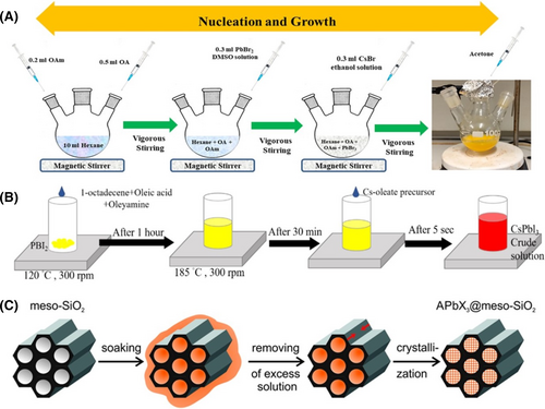
Schematic diagram of the preparation method of 0D HPs. (A) Preparation of HP nanocrystals by LARP. Reproduced with permission.63 Copyright 2014, American Chemical Society. (B) Thermal injection method. Reproduced with permission.65 Copyright 2022, MDPI. (C) SiO2 mesoporous template method. Reproduced with permission.62 Copyright 2016, American Chemical Society.
2.2 Defects and stability of HPs
2.2.1 Defects
Like all crystalline materials, defects will be inevitably introduced during the preparation of HPs. The defect state density of HP films is two orders of magnitude higher than that of single-crystal perovskites, indicating that defects are mainly distributed at the grain boundaries and crystal surfaces.42, 67, 68 Among them, defects at the grain boundaries are the most serious and active, which are the intrinsic causes of device and performance degradation.69-73 The defects in HPs can also be divided into 3D, 2D, 1D, and 0D defects, and the specific defect types and the corresponding passivation methods are shown in Figure 6.74
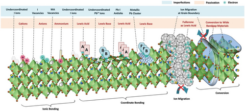
Defects in perovskite membranes and their passivation methods. Reproduced with permission.74 Copyright 2019, The Royal Society of Chemistry.
3D defects
They include precipitates, second phases, lead clusters, etc. The macroscopic expression of 3D defects is cracks or pinholes on the surface of the HP film.75-77
2D and 1D defects
2D defects refer to grain boundaries and surface defects, which are composed of a combination of point defect arrays, as well as a large number of uncoordinated ions and suspended bonds due to lattice breakage. The 2D defect density of polycrystalline perovskite films is generally 1016 cm−3, which is about 5 orders of magnitude higher than that of single-crystal perovskites. 1D defects refer to the dislocations, which are formed by the shifts or misalignments of certain atoms in the crystal.78, 79 The reason for the existence of these defects in HPs may be ascribed to the surface evaporation of organic components with low thermal stability and low formation energy during annealing.75
0D defects
They refer to point defects caused by vacancy, anti-site substitution, and interstitial sites, which are divided into intrinsic defects or non-intrinsic defects, caused by exogenous impurities or doped atoms. There are two typical intrinsic point defects, namely the Schottky defect and the Frenkel defect. Both Schottky defect and Frenkel defect are caused by vacancies, which are formed by ion immigration. The difference is that the ions migrated out of the lattice for Schottky defects, while the ions left the lattice points but still occupied the interstitial position within the lattice for Frenkel defects. It is reported that, there are twelve kinds of intrinsic point defects in CH3NH3PbI3: VMA, VPb, and VI vacancies, MAi, Pbi, Ii, and PbI interstitial sites, and MAPb, MAI, PbMA, PbI, IMA, and IPb anti-site substitutions.74
The above defects can also be further classified into shallow and deep level defects, depending on the relationship between their ground-state energy levels and valence or conduction band edges. The difference between the ground state energy level of the shallow level defect and the valence or conduction band edge is equal to or less than the thermal excitation energy kBT at room temperature. The difference between the ground state energy level and the valence band or conduction band edge energy level of the deep level defect is much larger than that of the kBT.80 Carriers trapped by shallow level defects are easily released and contribute little to nonradiative recombination, such as MAi, VPb, MAPb, Ii, VI, and VMA.73, 81 Non-radiative recombination is serious in deep level defects, which can capture charge carriers with opposite charges, such as making uncoordinated Pb2+ and uncoordinated I− into metallic Pb and I elements, respectively, accelerating the degradation of perovskite films.68 Generally, low-coordinated Pb2+ or halogen ions, Pb clusters, and Pb-I anti-site substitutions defects formed during crystal growth tend to form deep level defects.74
2.2.2 Stability
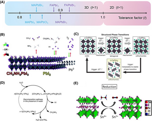
(A) Tolerance factors of 2D and 3D perovskites. Reproduced with permission.75 Copyright 2022, Willey-VCH. (B) The photodecomposition and thermal degradation processes of MAPbI3 contribute to the irreversible decomposition of organic volatile gas species (CH3I+NH3), reversible decomposition (CH3NH2+HI), and reversible production of I2 and nonvolatile Pb0 under light or mild thermal conditions. Reproduced with permission.85 Copyright 2008, The Royal Society of Chemistry. (C) The crystal structure of cubic, tetragonal and orthorhombic phases and their relative phase transitions. Reproduced with permission.86 Copyright 2009, Science. (D) Possible decomposition pathways of HPs in the presence of water. Reproduced with permission.88 Copyright 2004, American Chemical Society. (E) Suggested mechanism of hydrazine vapor reaction with Sn-based perovskite materials. Reduction process: 2SnI62− + N2H4 → 2Sn42− + N2 + 4HI. Reproduced with permission.91 Copyright 2006, American Chemical Society.
The stability of HPs is usually determined by intrinsic and external factors. Intrinsic factors, also known as intrinsic instability, originated from the instability of perovskite materials themselves, such as thermal instability, phase instability, and chemical instability. External factors include high humidity, high temperature, strong light, oxygen enrichment, and other conditions that could accelerate the decomposition of perovskite materials.84 Thermal instability is a result of the increase in temperature due to the thermal effects of light or current during the operation of devices. For example, MAPbX3 can decompose into volatile CH3I and NH3 gases at high temperatures, or reversibly decompose into CH3NH2, HI, I2, and nonvolatile Pb0 at relatively low temperatures (Figure 7B).85 The phase stability is determined by the tolerance factor t as described above, and the formation of a stable crystal structure is facilitated by an appropriate t. Generally, non-perovskite structures will be formed when t < 0.8 and low dimensional perovskites will be formed when t > 1.21. For example, CsPbI3 has a t of 0.8, which is on the edge of phase transition. Therefore, the black photoactive α phase will change to the yellow δ phase at room temperature (Figure 7C).86, 87 Chemical instability refers to the ionic properties of chemical bonds in HPs, which can easily absorb moisture in the environment and result in the degradation of HPs. For example, MAPbI3·H2O and (MA)4PbI6·2H2O species will be formed when MAPbI3 is exposed to a little water vapor, facilitating the formation of grain boundaries. When the water is excessive, it eventually leads to irreversible degradation of MAPbI3 to form MA and PbI2 (Figure 7D).88, 89 Stabilizers or reducing agents, such as SnF2-pyridine complex,90 hydrazine vapor,9 ammonium hypophosphatite,91 ascorbic acid,92 formamidine sulfonic acid,2 and tin powder, can effectively inhibit the formation of Sn4+ defects (Figure 7E).93, 94
3 BASIC KNOWLEDGE OF MEMRISTORS
3.1 The development history of memristors
There are four basic variables in the circuit: voltage (v), current (i), charge (q), and magnetic flux (φ), which can be combined in pairs to obtain known resistance (R, determined by v and i), capacitance (C, determined by v and q), and inductance (L, determined by i and φ). In 1971, based on the symmetry and completeness of the relationship between the circuit variables, Leon O. Chua predicted a fourth device defined by “φ” and “i”, the memristor (Figure 8A).95 Different from the fixed resistance values of ordinary resistors, the resistance value of a memristor is determined by the applied “v” or “q” flowing through, and it is nonvolatile. Under the stimulation of current or voltage, the resistance value of the memristor will switch between a high resistance state and a low resistance state. Generally, when the memristor changes from HRS to LRS, it is called the “SET” process, and when the memristor changes from LRS to HRS, it is called the “RESET” process. When the SET and RESET of the memristor are carried out under the same voltage polarity, it is called unipolar resistive behavior (Figure 8B). Correspondingly, when the SET and RESET of the memristor are carried out under different voltage polarities, it is called bipolar resistive behavior (Figure 8C). According to whether there is a clear threshold switching voltage in the resistance change, memristors are divided into the digital memristors and analog memristors, which show significant sudden changes and slow changes in resistance in the I-V curve, respectively (Figure 8D,E).
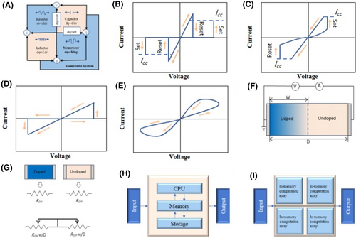
(A) Four basic circuit components and their relationship diagrams. (B) Schematic diagram of unipolar resistive behavior. (C) Schematic diagram of bipolar resistive behavior. (D) Resistance switching behavior of digital memristor. (E) Resistance switching behavior of the analog memristor. (F) Diagram with a simplified equivalent circuit. V, voltmeter; A, ammeter. (G) Equivalent circuit symbols for doped and undoped portions of the device. (H) Von Neumann architecture. (I) In-memory computing architecture.
In 2008, Hewlett–Packard's Lab successfully verified the existence of memristor for the first time, which has a sadwich-like structure of Pt/TiO2/Pt. The device structure and equivalent circuit diagram are shown in Figure 8F,G.96 In 2009, Ho et al. took the lead in characterizing memristor-based nonvolatile memory, implementing a binary memory cell using a single memristor.97 In 2010, Borghetti first proposed the use of memristors to realize the fusion of logic operations and storage.98 The difference between the von Neumann architecture and the memory and computing integrated architecture is shown in Figure 8H,I. In 2013, Thomas first described how biological synaptic behavior can be mimicked by a memristor-based artificial neuromorphic network, namely the historical electrical pulses applied to the memristor corresponding to the stimulus signals in biological synapses. Moreover, the synaptic connection weight varies along the external stimulus pulses.99 In 2020, Wu et al. developed the first multi-array memristor-based memory-computing integrated system with low hardware cost and power consumption. The energy efficiency of it is two orders of magnitude higher than that of a graphic processing unit (GPU) when processing complex calculations by convolutional neural networks (CNNs).100 In the same year, Li et al. experimentally demonstrated a complete memristor-based neural network, with power consumption much lower than traditional integrated circuit chips, which can accurately complete digital image recognition tasks.101 At present, companies such as Panasonic, Adesto Technologies, Crossbar, and Micron have initially realized the commercial application of memristor memory chips, but analog memristor chips have not yet been commercialized.
3.2 Structure of memristors
As a new type of electronic device, the structures of HPs-based memristors are usually 2T or three-terminal (3T). A HPs-based memristor with a 2T structure consists of the substrate, BE, HPs active layer, and TE, and sometimes a modification layer can be added between the electrode and the HPs active layer. The substrates of the memristors are usually silicon (Si) or glass. The BE materials are normally metal (gold (Au), silver (Ag), etc.) or conductive metal oxide (indium tin oxide (ITO), tin fluoride dioxide (FTO), etc.). The TE materials are generally metals, including both active metals such as silver (Ag), aluminum (Al), copper (Cu), and nickel (Ni), and inert metals such as gold (Au), platinum (Pt), tungsten (W), etc.102 The 2T memristor is further divided into a dot structure and a cross-array structure according to the shape of the TE and the BE (Figure 9A,B). In the dot structure, the BE is prefabricated on the substrate, while the TE is deposited on the HPs layer by thermal evaporation and electron beam sputtering under the action of a mask. The advantage of the dot structure is that the number of devices per unit area is large, and the BE does not need to be specially designed. However, the dot structure does not lead to electrodes at the edge of the device, so it is inconvenient to integrate. The cross-array structure is the mainstream device structure, which realizes the array by itself through the vertical crossing of the TE and the BE. It should be noted that after the preparation of the perovskite layer, an area around the device should be wiped by solvent or scraped with a knife to expose the BE.

Structure diagrams of halide perovskite memristor. (A) Point shaped structure. (B) Cross array structure. (C) Transistor structure.
The 3T structure of HPs memristor is also called transistor, and the perovskite layer is usually fabricated on a substrate of silicon (Si) and silicon dioxide (SiO2) (Figure 9C). However, HP is generally not applied directly to transistor channels, where higher operating voltages are often required. In practice, HP mainly acts as a floating gate layer or forms a heterojunction with organic materials to absorb light and separate charges. Although the 3T structure is more complex to fabricate than the 2T structure, it has the advantage of being compatible with the current transistor manufacturing process.
3.3 Performance parameters of memristors
3.3.1 Switching current ratio (ION/IOFF)
Switching current ratio refers to the ratio of current in the high-impedance state to the low-impedance state, namely ION/IOFF. The higher the ION/IOFF, the higher the read and write accuracy of information. In addition, high ION/IOFF simplifies circuits by reducing the use of amplifiers in the circuit.
3.3.2 Threshold voltage (Vth)
Vth refers to the switching voltage of the memory device, including the write voltage (VSet) and the rewrite voltage (VReset), corresponding to the operating voltages that transform the HRS to the LRS and LRS to HRS of the device, respectively. A lower operating voltage means lower power consumption, so the lower the Vth the better.
3.3.3 Access time
Access time refers to the time of reading or writing of information, manifesting the operating speed of memristors. The magnitude of the access time can be measured by changing the pulse width of the write or read voltage. The faster the read and write speeds, the higher the efficiency and responsiveness of memristors. The current memory devices typically require switching and reading times less than 1 μs.
3.3.4 Retention time
Retention time refers to the ability of memristors to retain data. The higher the retention time, the stronger the long-term memory capacity of the device.103
3.3.5 Cycling endurance
It refers to the highest value of reversible cycles in which the device can change steadily between HRS and LRS. High cycling stability can ensure the storage security of data.104
3.3.6 Multi-resistance states
Ideally, a memristor should exhibit more than 100 (or 6 bits) distinguishable analog resistance states to ensure the accuracy and robustness of neuromorphic operations. It can also reduce the power consumption, latency, and device area ratio caused by frequent analog-to-digital conversion.105
3.3.7 Power/energy consumption
4 RESISTANCE SWITCHING MECHANISMS AND APPLICATIONS OF HPs-BASED MEMRISTORS
4.1 Resistance switching mechanisms of HPs-based memristors
At present, the resistance switching mechanisms of HPs-based memristors are still not very unified. According to the literature, we can simply classify them into the valence change mechanism (VCM), the electrochemical metallization mechanism (ECM), and the interfacial charge transport.
4.1.1 VCM
VCM means that ions with lower activation energy (such as I− and Br−) migrate along the defect vacancies by applying external voltage, and finally form a conductive channel connecting the BE and the TE.106 Typically, the conductive channel forms or breaks when a forward or reverse voltage is applied, and the device completes the transition from the HRS to the LRS or LRS to HRS (Figure 10A,B).107 In 2015, Xiao et al. first discovered the obvious photocurrent hysteresis in MAPbI3 solar cells and speculated that it was related to the migration of I−.108 In the same year, Eames et al. measured the activation energies of the above photocurrent hysteresis to be 0.60–0.68 eV, which is very close to the calculated I− migration energy of 0.58 eV. However, the migration energy for MA+ and Pb2+ are 0.84 and 2.31 eV, respectively, suggesting that the photocurrent hysteresis should be caused by I− migration. The migration paths of I−, Pb2+, and MA+ between adjacent locations in the lattice are shown in Figure 10C,D.27 In 2016, Gu et al. reported the first flexible PET/ITO/MAPbI3/Au memristor, proposing that the typical bipolar memory behavior of this device is caused by halogen ion migration. Specifically speaking, with the increase in the applied voltage, VI vacancies aggregate near the negative polarized electrode, finally forming VI filaments that connect from the negative polarized electrode to the positive-biased electrode and allow the transition of HRS to LRS of the device.109 Meloni et al. also confirmed through experimentation and theoretical calculations that ion migration is the main working mechanism of the electric hysteresis phenomenon of perovskite solar cells.110
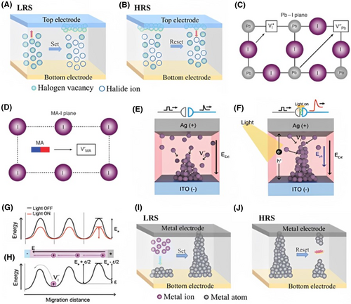
(A, B) Set and reset processes under halogen ion migration mechanism. Reproduced with permission.107 Copyright 2023, The Royal Society of Chemistry. (C) I− migration along the edges of the octahedron; Pb2+ migrates along the diagonal of the cubic unit cell. Reproduced with permission. (D) MA+ migration into a neighboring vacant A-site cage. Reproduced with permission.27 Copyright 2015, Nature. (E) Schematic diagram of the proposed mechanism of VI migration to form conductive channels under dark conditions. (F) Schematic diagram of the proposed mechanism of VI migration to form conductive channels under light conditions. (G) The change in the Ea as a function of the migration distance of VI in the presence of an external electric (or photogenerated electric) field. (H) Ea when light is OFF (black) and ON (red). Reproduced with permission.111 Copyright 2009, Willey-VCH. (I, J) set and reset processes under metal ion migration mechanism. Reproduced with permission.107 Copyright 2023, The Royal Society of Chemistry.
In addition, light can also assist ion migration. Ham et al. showed in the reported vertical Ag/MAPbI3/ITO synaptic device that the application of a light stimulus produced a photogenerated electric field in the same direction as the positive bias, resulting in an enhanced driving force for VI migration to ITO.111 Figure 10E,F illustrate the proposed mechanism of how devices form conductive channels through VI migration under dark and light conditions, respectively. When the device is illuminated by light, the photogenerated electric field Eph may be in the same direction as the external applied electric field Eext. This is because the different built-in electric fields on the perovskite layer and the electrode cause electron-hole separation. The increased electric field of Eph enhances the driving force (zeE) of VI migration to the ITO electrode, causing a lowering of the activation energy (Ea) by −ε∕2(ε ∝ zⅇE) (Figure 10G).112 Note that z is the ionic charge, e is 1.60 × 10⁻²³ C, and E is the applied electric field. Furthermore, it has been reported that Ea itself can be further reduced with increasing light intensity due to the structural transformation or weakening of the bond strength of perovskite film caused by photo-induced charge carriers (Figure 10H).113
4.1.2 ECM
ECM refers to the case when an active metal is used as an electrode, under the action of an electric field, the active metal will first be oxidized into metal cations nearby the positive electrode, then the metal cations migrate through the perovskite layer, and are reduced into metal filament once they reach the negative electrode and form a conductive channel between the two electrodes.106 As a result, the device switches from HRS to LRS. When a reverse voltage is applied to the metal electrode, the metal conducting wire melts and breaks due to Joule heating, causing the device to switch from LRS to HRS. Therefore, the conductive metal filament channels can form or break when an external voltage in different direction is applied (Figure 10I,J).107 Yan et al. demonstrated the ECM in 2016. Through experiments, they showed that the memristive behavior is only observed when active metals are used as electrodes. Furthermore, they found that the resistance of the low-resistance state increases with temperature, indicating a metal-dependent nature of the device resistance.114
In addition, Sun et al. found a competition between metal ion migration and halogen ion migration in Ag/CH3NH3PbI3/Pt-structured memristor.115 When the film thickness of the perovskite layer is about 90 nm, Ag CFs and VI CFs appear simultaneously. However, when the film thickness of the perovskite layer increased to hundreds of nanometers, VI vacancies dominated the formation and fracture of conductive filaments.
4.1.3 Interfacial charge transport mechanism
The interfacial charge transport mechanism is mainly caused by the energy level barrier between the electrode and the resistance or modification layer, which is different from the ion mobility mechanism. In 2018, Zhou et al. reported a memristor with a structure of Au/MAPbI3-xClx/FTO (Figure 11A).116 As the positive voltage applied to the Au electrode increases to 1.5 V, holes can be injected from the Au electrode to the CH3NH3PbI3-xClx/Au interface and filled into the hole trapping sites. With the accumulation of holes between the CH3NH3PbI3-xCl = /Au, the Fermi level of the perovskite shifts toward the valence band, resulting in a lower Schottky barrier. Then, the contact between the perovskite and Au electrodes becomes quasi-ohmic and the device switches to LRS. The injected holes can be stably trapped by the deep level defects, so the LRS can be retained even after removing the electrical bias. When a negative bias is applied to the gold electrode, the holes can recover from the trapped states at the interface of CH3NH3PbI3-xClx/Au. The Schottky barrier between the electrode and perovskite layer becomes high, and the device returns to its original state (HRS) (Figure 11B). Moreover, because the Schottky barrier at the interface can also be modified by trapping the photogenerated carriers, a bias as low as 0.1 V is required to complete the SET operation of the device upon the illumination of light (Figure 11C). This process shows that the Schottky junction plays a decisive role in the resistance switching mechanism. In addition, in the memristor of Al/Cs0.05(FAxMA1-x)0.95PbIyBr3-y/FTO structure reported by Wang et al., it was also confirmed that the photogenerated charge carriers in perovskite drift through the depletion region of the Schottky potential barrier, generating photocurrent and at the same time, neutralizing some of the defects near the interface, and finally reducing the electron potential barrier height.117 Ma et al. used a simple air exposure method to adjust the interfacial states of the perovskite layer and found that devices could exhibit a transition from lag-free to bipolar RS.118 After exposing the device to air for 7 days, the surface work function of the perovskite film decreased from the initial 5.3–4.5 eV. The Schottky barrier lowering at the Au/MAPbI3 interface first forms an Ohmic contact and eventually an inverted Schottky junction, and the device thus exhibits bipolar resistance switching properties. In 2023, Yan et al. reported a memristor with structure of ITO/FA1−yMAyPbI3−xClx/(PEA)2PbI4/Au.119 A defect-modulated electron tunneling mechanism is demonstrated using the p-i-n junction model, and it is proven that the conductance state of the memristive device is determined by the defect concentration in the perovskite film near the electrodes.

(A) Schematic device structure of perovskite-based RRAM. (B) Electrical switching mechanism. (C) Photo-assisted switching mechanism including four states: (I) initial state corresponding to HRS: hole trapping centers located at the perovskite surface; (II) SET process: hole trap states are filled, shifting the Fermi level to the valence band; (III) remove light electricity: a lowered barrier and quasi ohmic contact are created corresponding to LRS; and (IV) electrical reset: holes are extracted from the trap states and a transition from LRS to HRS occurs. Reproduced with permission.116 Copyright 2018, Willey-VCH.
4.2 Application of HPs-based memristors
4.2.1 Information storage and logical operation
The rise of AI represented by intelligent driving, edge computing, and mobile terminals has led to the explosive growth of data volume. The need for efficient information storage and logical computation drives researchers to explore emerging technologies. Halide perovskite memristors have attracted much attention due to their unique properties such as high-density integration, multi-stage storage, and scalability. By using these advantages, halide perovskite memristors are expected to change the current situation of low storage density and insufficient computing power in traditional electronic devices. In 2019, Cheng et al. used Cs2AgBiBr6 for the first time to fabricate a memory with highly robust properties that maintained memory behavior under humidity up to 80%, temperature up to 453 K, an alcohol burner flame for 10 s, and 60 Co γ-rays at a dose of 5 × 10⁵ rad.120
This exceeds most halide peroxide memristors. The device “write” and “erase” operations can be repeated more than 1000 times, and the ON/OFF resistance ratio is always greater than 10. Each state can last for more than 105 seconds without significant degradation, outperforming most other hybrid perovskites. If four compliant currents (100, 3, 1, and 0.3 mA) are used during the voltage sweep, four different on-state conduction levels are obtained, indicating the potential application of these dual perovskites for multilevel information storage. In 2022, Liu et al. successfully fabricated EGaIn/MA0.85Cs0.05PbI3/PEDOT:PSS/ITO memristor under ambient conditions, based on the remarkable structural stability of hybrid A-site cationic perovskites, which are insensitive to heat and moisture.121 The device exhibits nonvolatile bipolar RS performance with low SET/RESET voltage (∼0.54/−0.66 V), stable durability (2 × 10³ cycles), high electrical and optical ON/OFF ratios (>0.5 × 10⁴ and 105), and long data retention (2 × 10⁴ s). Importantly, four HRS and one LRS were obtained in the MA0.85Cs0.05PbI3 memristor by applying different RESET stop voltages as well as electrical SET and optical RESET operations. Among them, under the condition of only electrical stimulation, the device can give three HRS (HRS1, HRS2, and HRS3) and one LRS, and their distribution is shown in Figure 12A. In addition, by exploring the optical response of the device, the authors found that a higher resistive state of HRS4 could be obtained and remained stable for a long time, as shown in Figure 12B. In order to apply photoelectric synergy to multistage storage, the authors performed cycle durability tests, as shown in Figure 12C. The results showed that no failure of electrical SET or optical RESET was found during the whole period. In addition, Figure 12D also shows that the LRS, HRS1, HRS2, HRS3, and HRS4 of the device can retain 2 × 10⁴ s at a read voltage Vread of −0.1 V. The MA0.85Cs0.05PbI3 memristor, with excellent durability and reproducibility is able to avoid error rates and achieve five-stage storage. The above studies show that HP devices not only realize data storage, but also have potential applications in optical digital computing and optical quantum information.
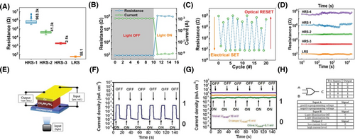
(A) Resistance distribution of four-level resistance states of the MACsPbI3 memristors. (B) Evolution of the device current and resistance under light illumination. (C) Cycling electrical SET and optical RESET RS behavior. (D) Retention characteristics of the five-level resistance states based on the electrical SET and optical RESET RS behavior. Reproduced with permission.121 Copyright 2022, Elsevier. (E) Schematic diagram of the light illumination induced logic OR gate. (F) I-T response of a device programmed to HRS under illumination of an optical ON/OFF switch with a read voltage of 10 mV. (G) I-T response of a device programmed to LRS under illumination of an optical ON/OFF switch with a read voltage of 0.1, 1, or 10 mV, respectively. (H) Logic or device state diagrams of two input sources and one output terminal. For input source A, the electric field, the signals “1” and “0” represent negative and positive fields, respectively. For the input source C, which is illumination, the signals “0” and “1” indicate the light off and on states, respectively. Reproduced with permission.122 Copyright 2015, The Royal Society of Chemistry.
Benefiting from the excellent light response of HP materials, Lin et al. designed and prepared a light-sensitive logic gate device (the inputs A and B are the electric and light stimuli, respectively, and the output C is the current level) ITO/PEDOT: PSS/CH3NH3PbI3/Cu with OR gate characteristics in 2015 (Figure 12E).122 Figure 12F shows the 6 cycles of the I-T response when HRS and LRS of the device are switched. It can be seen that the photocurrent shows a switching ratio greater than 103 and a certain repeatability under the solar simulator (100 mW cm−2) irradiation, the switching ON/OFF of 8/18 s, and the Vread of 10 mV. However, under LRS, the device does not exhibit a significant light response, as shown in Figure 12G. Therefore, based on the above phenomenon, the photo-induced logic “OR” gate shown in Figure 12H can be designed (the input A and B are electric field and illumination, respectively, and the output C is current). For input A, the positive voltage is defined as signal “0” and the negative voltage is defined as signal “1”. For input B, the light off is defined as signal “0” and the light on as signal “1”. For output C, low current is defined as signal “0” and high current as signal “1". Therefore, the device can output signal “1” when one or two signals “1” are input, and output signal “0” when two signals “0” are input. Finally, the device realizes the operation of logic “OR” gate. In 2020, Hao et al. constructed the DPPDTT/CsPbBr3/QDs-PST 3T device by a simple solution spin-coating process.123 The basic AND and OR logic functions were successfully simulated by using 450 and 500 nm optical input signals. Specifically, the ΔEPSC of 5 nA set to the threshold that defines the output state. At a weak light intensity of 0.02 mW cm−2, the ΔEPSC is greater than the threshold when two photon input signals are applied simultaneously, which indicates that the AND logic function is achieved. When the light intensity is increased to 0.3 mW cm−2, the ΔEPSC is larger than the threshold whether one or two light pulses are used, which proves the realization of the OR logic function.
4.2.2 Artificial synapse and pattern recognition
Inspired by the fast memory computing and low-power information processing modes of the human brain, Caver Mead first proposed the concept of neural mimic computing.124 The advantage of neuromorphic computing is that it breaks the traditional memory and computing separation architecture and achieves highly parallel information processing by distributing computing tasks among multiple artificial neurons with integrated memory and computing functions. As a bridge between neurons, the artificial synapse is the most critical hardware unit to construct an artificial neural network, and its most critical feature is synaptic plasticity. Among the many hardware components used to implement neural mimic computing, the HPs-based memristor has become the most competitive choice due to its advantages of in-memory computing, low power consumption, and high-density integration. Functionally, HPs-based perovskite memristors can highly mimic neural synapses and achieve a variety of synaptic plasticity. Array-based halide perovskite memristors can perform multiply and accumulate calculations (MAC) in one step, which is the same MAC operation required for neural networks. These properties allow artificial synapses fabricated from HPs-based memristors to be used in constructed neuromorphic networks and are eventually applied in digit recognition, artificial vision systems, artificial pain sensor, etc.
In 2016, Xu et al. prepared the first HPs-based artificial synapse with CH3NH3PbBr3 and successfully simulated the excitatory postsynaptic current, PPF, STP, LTP, and STDP behaviors of biological synapse.125 Then in 2018, Wang et al. reported a 3T Si/SiO2/MAPbBr3 (QDs)/(PMMA)/pentacene/Au neuromorphic device to simulate synaptic connectivity rules in the human brain such as SRDP, STP, and LTP through optical modulation. The energy consumption of this photo synaptic transistor is calculated to be 1.4 nJ event−1 at a light pulse duration of 1 s. The energy consumption of this device can even be decreased to the level of fJ when the light pulse duration is reduced to 0.1 ms.126 In 2020, Zeng et al. fabricated a device with Ag/PMMA/MA3Cu2I5/ITO structure, which exhibited bipolar RS behavior, low operating voltage (<±1 V), large switching ratio (102), stable cycle durability (100 cycles) and long retention time (>104 s).127 Subsequently, the device is further applied to the Modified National Institute of Standards and Technology (MNIST) database, a handwritten digit recognition library commonly used in neuromorphic computing. In the adopted multilayer perception (MLP), the classification error between the correct number and the output number is used, and the synaptic weight is changed to make the error smaller. In the MLP, 28 × 28 pre-neurons in the input layer correspond to 28 × 28 MNIST handwritten images, the hidden layer has 300 neurons, and the output layer has 10 neurons for corresponding to 10 digits in the handwritten dataset. During 6000 iterations of training, the authors used gradient descent combined with the conductance change curve of experimental data to update the weights of synapses. Finally, it was successfully demonstrated that the artificial neural network (ANN) using Ag/PMMA/MA3Cu2I5/ITO devices as artificial synapses can achieve a recognition rate of up to 95%, which is comparable to the 97% recognition rate achieved by pure software simulation. In the same year, Yang et al. proposed a self-powered artificial retinal sensing system using ITO/CsPbBr2I/poly (3-hexyl thiophene) (P3HT)/Ag devices as optical synapses and in combination with silicon-based solar cells (Figure 13A,B).128 Solar cells are used to receive external optical signals and convert them to electrical signals, and changes in conductance/resistance of the HPs-based memristor are treated as enhancement or reduction of synaptic weights. Figure 13C shows the HPs-based solar cells as convolutional neural networks (CNNs) for image preprocessing. The pattern recognition process of the self-powered artificial retinal perception system at the hardware level is as follows (Figure 13D): light is first input to the solar cell array and generates an electrical signal, and then the memristor array receives the electrical signal for image preprocessing. Finally, the output image of the memristor array is input into the ANN twice and recognized by the gradient descent iteration. In addition, the authors constructed a 784 × 25 × 10 three-layer ANN to recognize the digits “1”–“9”, and the results show that the background noise of the preprocessed image is basically eliminated (Figure 13E right). Moreover, after 180 training cycles, a recognition rate of 86.55% can be achieved (Figure 13F). This experiment proves that the HPs-based memristor can realize the function of CNN feature extraction in the artificial vision system, improve the recognition rate, accelerate the recognition speed and reduce energy consumption.
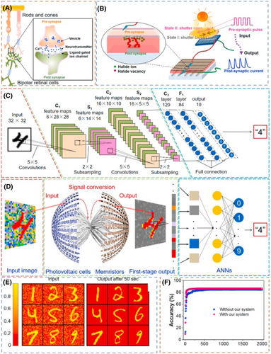
Self-powered artificial retina perception system. (A) The schematic illustration of biological synapses between rods (or cones) and bipolar retinal cells. (B) The illustration of self-powered artificial synapses of the retina perception system based on HPs memristors. (C) The diagram of CNNs. The input information is given in Figure “4”. (D) The illustration of the image preprocessing based on our self-powered artificial retinal perception system and subsequent ANNs for image recognition. (E) The contrast enhancement and the denoised effect of our self-powered artificial retina perception system when the irradiation intensity was considered. Left: the input image. Right: the output image after 50 s based on the fitting current-wavelength curve of our self-powered artificial retina perception system. (F) Comparison of the image recognition rate with and without image preprocessing based on our self-powered artificial retina perception system when the irradiation intensity was considered. Reproduced with permission.128 Copyright 2020, Elsevier.
4.2.3 Hardware security
The development of electronic devices makes people highly reliant on network devices to process confidential information, including various private information in daily life, such as account passwords, biometric information, verification information, etc. Information security requires the development of hardware solutions while addressing the risk of information leakage at the software level. Traditional hardware encryption techniques usually rely on nonvolatile memory arrays to store the keys used by different encryption algorithms.129 Physical unclonable function (PUF) is one of the most promising hardware encryption primitives, which can dynamically generate random and unique secret bit strings.130, 131 In 2021, Kim et al. first proposed to exploit the randomness of the physical behavior of switches based on 1D HPs-based memristors as an excellent entropy source for security primitives for key generation and device authentication (Figure 14).132 In this experiment, the device fabricated using propyl pyridinium lead iodide (PrPyrPbI3) exhibits excellent bipolar resistive switching behavior. The high switching ratio of 105 ensures a wide programming margin, thereby enhancing the reliability of the PUF. In addition, the device can exhibit a retention time of about 104 s over 450 switching cycles, which proves the stability of information storage. Measurements of a prototypical 1 KB propyl pyridinium lead iodide (PrPyrPbI3) weak memristor PUF with a differential write-back strategy reveal near ideal uniformity, uniqueness, and reliability without additional area or power overheads. Cycle-to-cycle write variability for several weeks enables reconfigurability, and in-memory computing supports powerful recurrent PUF structures to thwart machine learning attacks. Compared with the more mature oxide RRAM PUF, this device shows unique reconfigurability and write-back. This discovery will play an important role in promoting product authentication and identity recognition in the field of integrated circuits (IC).
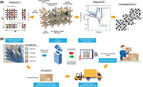
(A) HPs possess a rich reservoir of intimately coupled charge transport properties that could serve as sources of entropy to design new kinds of PUFs. (B) Concept schematic of product authentication. Reproduced with permission.132 Copyright 2021, Nature.
5 CONCLUSIONS AND PERSPECTIVES
In summary, we discussed the basic knowledge of HP materials and memristors in detail, as well as the latest research progress of HPs-based memristors. Due to the rich and flexible adjustability of structure, composition, size, and morphology, HPs-based memristors show diverse and excellent photoelectric responsive characteristics, which can realize logic operation and information storage, artificial synapse simulation, and act as entropy sources under low operating voltage. In addition, simple solution processability and defect regulation can prepare high performance HPs-based memristors with low power consumption.
Although the research on HPs-based memristors has made great progress in recent years, there are still many problems and challenges that need to be solved in the experimental stage. Here, based on the above discussion, we put forward several difficulties and research directions of HPs-based memristors for the consideration of researchers working in the fields of memristors and perovskites: (1) The stability of HPs undoubtedly has a huge impact on the performance of their electronic devices. Theoretically, the stability of HPs can be increased by lowering their dimensions, however, their conductivity will also be affected. In the future, the HPs-based memristor with high stability is still a big challenge that needs to be addressed. (2) Although the halogen ion migration mechanism is regarded as the mainstream mechanism for HPs-based memristors by virtue of grain boundary defects, the description of the influence of defect types and defect state density is still lacking. Future studies on the characterization of defect types and defect state density can help us to deeply understand the working principles of HPs-based memristor. (3) It is shown that deep level defects can aggravate the recombination of photo-generated charge carriers, thereby affecting the mobility and lifetime of charge carriers. However, in the research of photo-stimulated memristors, the influence of deep level defects on the resistive switching performance has not yet been disclosed. In addition, the coupling effect of light and electrical stimulation is also not clear. (4) The fabrication of HPs-based memristor array for application in in-memory computing and artificial retinal perception systems is still a technical challenge. The achievement of an exemplary HPs-based memristor array will provide great application perspectives for HPs in the field of AI.
Overall, based on their excellent intrinsic characteristics, the HPs-based memristors show excellent electrical, optical, and optoelectrical responsive resistive switching properties, allowing them to be utilized for logic operation, information storage, artificial synapse, neuromorphic computing, and hardware security. With the development of HP materials and memristors, we believe that HPs-based memristors might lead to great progress and provide an outlook for future innovations in HPs-based memristors for applications in AI, cloud computing, Internet of Things, and other fields in the future.
AUTHOR CONTRIBUTIONS
Xiaozhe Cheng: Conceptualization; Formal analysis; Methodology; Writing – original draft. Zhitao Dou: Conceptualization; Formal analysis; Methodology. Formal analysis; Methodology. Hong Lian: Formal analysis; Methodology. Zhitao Qin: Formal analysis; Methodology. Hongen Guo: Formal analysis. Xifeng Li: Formal analysis. Wai-Yeung Wong: Funding acquisition; Project administration; Resources; Supervision; Writing – review & editing. Qingchen Dong: Funding acquisition; Project administration; Supervision; Writing – review & editing.
ACKNOWLEDGMENTS
This work was supported by the financial support from the National Natural Science Foundation of China (Grant No.: 62174116 and 61774109) and the start-up fund from Shanghai University. Wai-Yeung Wong thanks the financial support from the RGC Senior Research Fellowship Scheme (SRFS2020-5S01), the Hong Kong Research Grants Council (PolyU 15307321), Research Institute for Smart Energy of Hong Kong Polytechnic University (CDAQ) and Ms Clarea Au for the Endowed Professorship in Energy (847S).
CONFLICT OF INTEREST STATEMENT
The authors declare no conflict of interests.
Biographies

Xiaozhe Cheng received his MS degree in Materials Science and Engineering from Taiyuan University of Technology (TYUT) in 2020. He is currently a joint PhD student of TYUT and Shanghai University (SHU) under the guidance of Prof. Qingchen Dong. His research interests focus on the design and synthesis of functional materials for memory devices and artificial neuromorphic computing.

Wai-Yeung Wong obtained his Ph.D. degree from the University of Hong Kong (HKU). He did postdoctoral works at Texas A&M University and University of Cambridge. He joined Hong Kong Baptist University (HKBU) from 1998 to 2016 and he now works as Chair Professor of Chemical Technology and Dean of Faculty of Science at the Hong Kong Polytechnic University (PolyU). His research focuses on synthetic inorganic/organometallic chemistry, especially aiming at developing metal-organic molecules and polymers for organic optoelectronics and metal-based nanomaterials.

Qingchen Dong obtained her Ph.D. degree under the tutelage of Prof. Wai-Yeung Wong in 2012 at Hong Kong Baptist University (HKBU). She also worked at Caltech with Prof. H. B. Gray from 2010 to 2011. She joined Taiyuan University of Technology (TYUT) from 2012 to 2021 and she now works at Shanghai University (SHU) as a full Professor. Her research involves the design and synthesis of functional organic and metallo-organic compounds for applications in data storage, artificial synapse and neuromorphic computing, optoelectronics, biomedicine, etc.
Open Research
DATA AVAILABILITY STATEMENT
Data are available on request from the authors.


