Halogen-free solvent processed organic solar sub-modules (≈55 cm2) with 14.70% efficiency by controlling the morphology of alkyl chain engineered polymer donor
Thavamani Gokulnath and Hyerin Kim contributed equally to this study.
Abstract
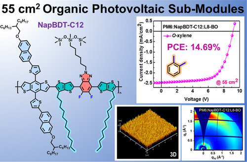
Goals of high efficiency, morphological analysis, and the ability to produce organic solar cell (OSC) sub-modules using halogen-free solvents are demanding. In this study, a robust conjugated polymer with thienothiophene π-spacer with pendant alkyl side chain (NapBDT-C12) was synthesized and used to fabricate sub-modules. Excellent efficiencies were demonstrated by a NapBDT-C12 integrated ternary blend, which was used to produce stable small-area-to-sub-module devices using O-xylene. The efficiency of the NapBDT-C12 added small-area ternary devices (PM6:NapBDT-C12:L8-BO) was 18.71%. Owing to the controlled homogeneity of the blend with favorable nanoscale film morphology, enhanced carrier mobilities, and exciton dissociation/splitting properties, contributed to the efficiencies of small-area-to-sub-module OSCs. Moreover, a 55 cm2 sub-module with an efficiency of 14.69% was accomplished by bar coating using O-xylene under ambient conditions. This study displays the potential of a ternary blend based OSC device to produce high efficiency scalable sub-modules at ambient conditions.
1 INTRODUCTION
Recent developments in organic electronics have sparked intense interest in the ideal device architecture and the underlying molecular design of novel organic semiconducting materials suitable for commercial large-scale thin film production. Organic solar cells (OSCs) are one of the most exciting renewable energy technologies because of their exclusive features, which include flexibility, stretchability, light weight, affordability, and vibrant hues.1, 2 Over the past few years, rapid growth in the organic functional photoactive material and device engineering fields has been inextricably linked to advancements in organic photoelectric devices, made possible by the emergence of suitable conjugated donor/acceptor polymer or small molecules.3 In particular, higher power conversion efficiencies (PCEs) were achieved by improving exciton dissociation, charge transport, and mitigating the recombination by tuning the homogeneity of blend films, and thus, controlling molecular orientation and crystallinity.4-7 Due to innovative active layer material and rapid device engineering developments, the PCEs of small-area and sub-module OSCs have now exceeded >19 and >14%, respectively.8-12 It has been well reported that OSCs produced using halogenated solvents exhibit suitable active layer morphology. However, halogenated solvents are highly toxic to humans and the environment, and thus, cannot be used for large-scale manufacture.13-15 Therefore, for practical reasons, effective strategies must be devised to fabricate high-PCE OSCs using halogen-free solvents.
Currently, the PCEs of halogen-free solvent-processed large-area sub-module OSCs lag significantly behind those of halogenated solvent-processed OSCs.11, 16 This is primarily due to the uneven film topologies and poor film homogeneity of photoactive material blends in commonly used non-halogenated solvents. It has proven that it is difficult to control the molecular aggregation and crystallization dynamics of photoactive material composite during thin film formation, particularly for benchmark donor polymers (PM6, PM7, and D18), which often exhibit strong exciton formation and potential splitting efficiencies.3, 6 Conjugated polymers are prone to aggregate excessively when they processed from low-boiling-point halogen-free solvents, which often leads to severe film homogeneity and inferior OSC performance.12, 17, 18 Studies have shown that side chain modification provides a means of reducing the excessive aggregation in halogen-free solvents by reducing the excess polymer aggregations during film formation.11, 12, 19-22 However, non-ideal side chain also can be a bottle neck by prompting the high torsion and twisted polymeric structures. As such, the effects of film homogeneity on the stability and efficiency of large-area devices produced with scalable coatings have rarely been discussed, and thus, these relationships remain unclear. Alternatively, ternary strategy involving the judicious incorporation of a guest component (donor and acceptor) into the host binary blend has been able to adjust the excess molecular aggregation.5, 6, 23 Notably, majority of the sub-modules based on ternary blend possesses one donor and two acceptor systems. However, this could be attributed to the critical requirements of donor guest component including excellent halogen-free solvent processability and compatibility with the host polymer donor to enable the manipulation of molecular aggregation and film homogeneity. Henceforth, designing or understanding the delicate molecular engineering/behavior of guest components in ternary OSCs substantially important to export this technology from lab to fab scale. For example, in our most recent studies revealed that the addition of the alkoxynaphthylthiophene (ANPh) group to benzo[1,2-b:4,5-b′]dithiophene (BDT) based polymer donors proven to be an ideal guest components for constructing highly efficient halogen free solvent processed OSCs,24 perovskite solar cells (PSCs).25-27 On the other hand, increasing device area will exacerbate the limitations of standard active layer materials and reduce PCEs. Therefore, this topic requires further study in the context of developing high-PCE sub-module OSCs.
In this study, a polymer donor NapBDT-C12 has been incorporated into an optimized PM6:L8-BO binary blend to fabricate efficient small-area-to-sub-module OSCs using O-xylene (a halogen-free solvent). NapBDT-C12 exhibits subtle aggregation behavior as compared with the excessive aggregation shown by host PM6 when a commonly applied halogen-free solvent. Moreover, NapBDT-C12 showed impressive compatibility with host PM6 due to their aligned energy levels, miscibility, thereby amended the finely mixed nanoscale morphology. As anticipated, the addition of NapBDT-C12 suppressed aggregation of host in the ternary blend and resulted in a well-defined morphology with favorable phase separation. Furthermore, this morphologic improvement enhanced the exciton separation, mitigated trap density states, and reduced charge recombination. As a result, an impressive PCE of 18.71% (0.04-cm2) with open-circuit voltage (Voc) of 0.89 V, a short-circuit current density (Jsc) of 27.81 mA/cm2, and a fill factor (FF) of 75.45% was achieved for the ternary blend (PM6:NapBDT-C12:L8-BO). Moreover, the proposed strategy exhibits a superior advantage in extending device scales; and thus, a large-scale O-xylene-processed sub-module (55-cm2) delivers a high PCE of 14.69%. Our work demonstrates that incorporating NapBDT-C12 as the guest component is a feasible method to fabricate highly efficient ternary OSCs and scalable sub-modules processed from halogen-free solvent.
2 RESULTS AND DISCUSSION
2.1 Polymer donor design, synthesis and characterization
As shown in Figure 1A, molecular engineering of π-spacer has notable impact on the dipole moment of the triazole unit, which further effects in resulting polymer. We found siloxane terminated triazole acceptor unit containing NAP polymers are promising in both OSCs and PSCs.27 Thus herein, we further engineered it by introducing alkyl chain on thienothiophene spacer. Notably, sufficient alkyl chain on donor unit, spacer, and acceptor unit hampers better solubility for the resulting polymer compared to the thiophene/thienothiophene linked NAP polymers.
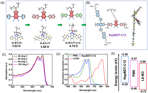
NapBDT-C12 polymer molecular structure is shown in Figure 1B. The UV–visible (vis) absorption spectrum of NapBDT-C12 in dilute solution (Figure S1) and film were systematically investigated. In dilute solution at room temperature (RT), the UV–vis absorption spectrum of NapBDT-C12 exhibited vibronic absorption peak at ~556 nm, indicating polymer backbone aggregation. The aggregation of NapBDT-C12 was studied using variable temperature-dependent UV–vis absorption spectra (Figure 1C). The A0-1/A0-0 vibrionic shoulder peaks of NapBDT-C12 were reduced at 100°C, indicating less aggregation at higher temperatures.24, 28, 29 The absorption spectra of PM6, L8-BO, and NapBDT-C12 films are shown in Figure 1D. PM6 and NapBDT-C12 exhibited absorption from 300 to 700 nm, which complemented that of acceptor L8-BO in the 600 to 1000 nm range. The maximum absorption peaks of NapBDT-C12 were located at 555 and 605 nm, and optical bandgap (Eg) of 1.90 eV, respectively (Table S1). The absorption coefficients of blended donor films were also determined; results are shown in Figure S2. A significant increase in the absorption coefficient of PM6:NapBDT-C12:L8-BO was observed in the wavelength range 300 to 850 nm. Presumably, this was caused by an improved molecular arrangement in the active layer caused by adding NapBDT-C12.24 Notably, PM6:NapBDT-C12:L8-BO had stronger absorption properties than the control binary film (PM6:L8-BO), which would favor higher current densities. The energy levels of PM6, L8-BO, and NapBDT-C12 are shown in Figure 1E.24, 27 The addition of NapBDT-C12 results in the formation of a cascade of energy levels between the three materials, facilitating exciton dissociation and charge transport and resulting in a higher Voc.30
The electronic characteristics and structural conformations of NapBDT-C12 were revealed using density functional theory (DFT) computations.24-26 As shown in Figure 1A, we found a linear increase in the dipole moment values (Si-BTzTh (3.62 Debye (D)) < Si-BTzTT (3.88 D) < Si-BTzTT-C12 (4.79 D)) upon engineering the π-spacer, and we anticipate respective changes will influence the resulting polymer. For example, dihedral angles between the electron-rich and electron-deficient units of NapBDT-C12 were computed (Figure S3), and the results obtained indicated the presence of π-π stacking and well-ordered molecular packing. The dipole moments of the ground (μg) and excited states (μe) were 4.10 and 16.46 D, respectively, and the difference (Δμge) between these dipole moments was 20.97 D, as calculated previous publication.31 NapBDT-C12 Δμge increases excitons along polymer chains and polarizability in the excited state, which promote the formation of a charge separation state.31, 32 Notably, the Jsc value of OSCs is significantly impacted by Δμge.
Contact angle testing was performed on active layer materials to investigate compatibilities.23, 33, 34 Results are provided in Figure S4 and Table S2. The surface energies of PM6, NapBDT-C12, and L8-BO films were 30.7, 31.6, and 32.9 mJ m−2, respectively, which suggested the possibility of forming an alloy donor between PM6 and NapBDT-C12. Meanwhile, thermogravimetric analysis (TGA) of NapBDT-C12 showed it was thermally stable at 408°C (Figure S5a). In addition, differential scanning calorimetry (DSC) showed no evidence of phase transition, indicating good phase stability from ambient temperature to 200°C (Figure S5b). The thermal stability of NapBDT-C12, as demonstrated by TGA and DSC, indicated commercial potential in high-temperature environments.
2.2 Photovoltaic properties of OSCs
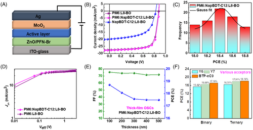
NapBDT-C12 was added to PM6:L8-BO, and OSCs with an inverted device structure (Figure 2A) were prepared using O-xylene. Relevant J–V curves and photovoltaic parameters are shown in Figure 2B and Table 1. After optimization, the PM6:L8-BO binary control device exhibited a PCE of 17.90% (Voc = 0.88 V, Jsc = 27.40 mA/cm2, and FF = 74.13%), which is consistent with a previous report.35 On the other hand, the NapBDT-C12:L8-BO device had a lower PCE of 9.70% due to its lower Voc, Jsc, and FF values (0.82 V, 19.92 mA/cm2, and 58.91%, respectively). The best ternary device was the PM6:NapBDT-C12:L8-BO blend with a weight ratio of 0.8:0.2:1.2 (Table S3 and Figure S6), which had an efficiency of 18.71% due to enhanced Jsc and FF values of 27.81 mA/cm2 and 75.45%, despite a slightly higher Voc of 0.89 V. Furthermore, ternary device incorporating 40% NapBDT-C12 provided a higher PCE of 17.83% and slightly lower Voc, Jsc, and FF values than the champion ternary OSC. Figure 2C shows a histogram of the PCEs of ternary devices and that NapBDT-C12-containing devices had better reproducibility. Next, we studied external quantum efficiency (EQE) spectra to confirm J–V results (Figure S7a). The binary and ternary films based on PM6:L8-BO and PM6:NapBDT-C12:L8-BO blends exhibited broad photoresponses in the range 350 to 950 nm, and their integrated current densities () were calculated at 26.21 and 26.28 mA/cm2, respectively, which aligned with J–V results. Notably, the EQE values of PM6:NapBDT-C12:L8-BO devices were significantly higher than that of PM6:L8-BO device, implying more efficient charge transfer and carrier collection due to altered molecular packing and intermolecular interactions.
| Active layera | Voc (V) | Jsc (mA/cm2) | FF (%) | PCEb (%) |
|---|---|---|---|---|
| PM6:L8-BO | 0.88 (0.85 ± 0.03) | 27.40 (27.23 ± 0.17) | 74.13 (73.73 ± 0.4) | 17.90 (17.73 ± 0.17) |
| PM6:NapBDT-C12:L8-BO | 0.89 (0.87 ± 0.02) | 27.81 (27.69 ± 0.12) | 75.45 (75.25 ± 0.2) | 18.71 (18.59 ± 0.12) |
| NapBDT-C12:L8-BO | 0.82 (0.78 ± 0.04) | 19.92 (19.73 ± 0.19) | 58.91 (58.41 ± 0.5) | 9.70 (9.50 ± 0.20) |
- a Processed using O-xylene.
- b Determined for an average of 15 devices.
A study was also conducted on the relationship between effective voltage (Veff) and photocurrent (Jph) to investigate exciton dissociations and charge transfers.23, 24 The saturation photocurrent densities of OSC devices were Jph and Jsat at 1 V (Figure 2D), indicating effective charge transfer/collection in active layers. The elevated exciton generation rates (Gmax) of PM6:L8-BO (the control binary device) and PM6:NapBDT-C12:L8-BO devices were 1.64 × 1028 and 1.76 × 1028 m−3 s−1, respectively. Also, PM6:NapBDT-C12:L8-BO had a higher exciton dissociation probability (98.37%) than PM6:L8-BO (94.54%), indicating maximum exciton dissociation at active layer interfaces. This was also supported by greater FF and Jsc values of the ternary blend devices. Charge recombination was investigated by examining relations between Voc and Jsc at different incident light intensities (Plight). The n values of PM6:L8-BO and PM6:NapBDT-C12:L8-BO were 1.15 and 1.07 kT/q, respectively (Figure S7b). According to the principle that a value approaching 1 suggests weaker trap-assisted recombination, NapBDT-C12 beneficially suppressed trap-assisted charge recombination. Moreover, the relation between Jsc and Plight follows the power-law Jsc∝, and an α value approaching 1 indicates less bimolecular recombination (Figure S7c). Note that the slightly higher α of the PM6:NapBDT-C12:L8-BO device (0.97) suggests weaker bimolecular recombination than that of the PM6:L8-BO (0.96) device. Superior exciton dissociation and charge extraction efficiencies and negligible charge recombination were responsible for the excellent performance of the PM6:NapBDT-C12:L8-BO device, which displayed higher FFs at low light intensities than the PM6:L8-BO device (Figure S7d). These results imply that PM6:L8-BO initiates free carrier recombination and causes FF losses as the number of free carriers increases with Plight. It follows that because of the strong intramolecular charge transfer (ICT) capability of NapBDT-C12, it produces more charge transport channels.
2.3 Active layer surface investigation
Atomic force microscopy (AFM) and transmission electron microscopy (TEM) were used to investigate the morphologies of blend films. As shown in Figure 3A–D, binary and ternary blend films had a fibrillar shape, which favors exciton dissociation and charge transfer, and the addition of NapBDT-C12 improved the topography and homogeneity of PM6:NapBDT-C12:L8-BO films. The surface roughness of this ternary film was 1.27 nm compared to a roughness of 2.16 nm for PM6:L8-BO film. Phase images of the PM6:NapBDT-C12:L8-BO film showed that the inclusion of NapBDT-C12 reduced molecular aggregation and improved the interpenetrating network shape of the PM6:L8-BO, which concurred with our TEM findings (Figure 3C,D). It has been shown that the morphology for OSCs depends greatly on the miscibility of the active layer material, and charge transport behavior may be affected by excessive active layer phase separation caused by poor miscibility. Flory-Huggins interaction parameters (χ) were calculated, and contact angle tests were performed to examine the miscibility of the two donors.23, 33, 34 Measured χ values for PM6/L8-BO, NapBDT-C12/L8-BO, and PM6/NapBDT-C12 were 0.527, 0.392, and 0.213, respectively. A low χ value often indicates a high degree of miscibility and a smoother surface (Figure S8), which would enhance the FFs and PCEs of OSCs.
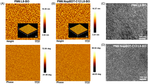
Figure 4 shows the 2D-grazing incidence wide-angle X-ray diffraction (2D-GIWAX) patterns and corresponding 1D profiles of pristine and blend films. 2D patterns of PM6 and NapDBT-C12 showed a typical preferential face-on structure, whereas that of L8-BO exhibited a highly crystalline structure (Figure 4A–C). 2D-GIWAX patterns of blend films showed similar preferential face-on structures (Figure 4D–F). It is clear that the crystalline reflections for L8-BO is fully disappeared in the 2D patterns for PM6:L8-BO and PM6:NapDBT-C12:L8-BO, indicating the L8-BO is fully miscible to the donor polymers.
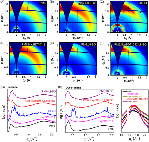
To analyze 2D-GIWAX patterns in more detail, corresponding in-plane (IP) and out-of-plane (OOP) 1D profiles were extracted and plotted in Figure 4G,H, respectively. PM6 and NapBDT-C12 films exhibited lamellar scattering peaks in the small q region, while a broad peak by the stacking of the molecule appears at the high q region. PM6 and NapBDT-C12 displayed a (100) peak at q = 0.29 and 0.17 Å−1, corresponding to d-spacing of 35.8 and 21.7 Å, respectively. In the donor blend film (PM6:NapBDT-C12), high-order diffraction peaks associated with NapBDT-C12 partially disappeared with the broadening and shifting of the (100) peaks of both PM6 and NapBDT-C12, indicating the two donor can form a mixed crystalline phase, which can be reduced domain sizes in the blend films (Figure S9).
Furthermore, PM6:L8-BO and PM6:NapBDT-C12:L8-BO blend films displayed similar features and exhibited a mixed packing motif and preferential face-on orientation. 2D-GIWAXD patterns revealed crystalline L8-BO peaks were much diminished in IP and OOP profiles, indicating full miscibility of L8-BO with the donor polymers. It should be noted that PM6:NapBDT-C12:L8-BO and PM6:L8-BO both produced a pronounced π-π stacking peak at qz = ~1.75 Å−1, corresponding to a d-spacing of 3.58 Å. As shown by 1D-profiles, the position of the π-π stacking peak of PM6, NapBDT-C12, and PM6:NapBDT-C12 shifted to the high q region from qz = ~1.69 Å−1, showing that the addition of L8-BO decreased the π-π stacking distance. This feature can facilitate excitation dissociation and charge transport in ternary blend films, which is in line with the higher Jsc and FF values of corresponding OSCs.
2.4 Charge carrier dynamics
The space charge limited current method was used to determine the hole mobilities (μh) and electron mobilities (μe) of the optimized OSC devices (Figure S10 and Table S4). μh/μe values for the PM6:L8-BO device were 7.33 × 10⁻⁴ cm2 V−1 s−1/8.27 × 10−4 cm2 V−1 s−1, respectively. The μh and μe values of the PM6:NapBDT-C12:L8-BO device were greater at 9.79 × 10⁻⁴ and 9.43 × 10⁻⁴ cm2 V−1 s−1, respectively, and the μh/μe ratio (1.03) more balanced, which contributed to the higher Jsc and FF values of the ternary device.
Photoluminescence (PL) was also measured, and time-resolved PL (TRPL) spectra were obtained to obtain insight into the fundamental mechanisms of these devices. Pristine and blended film PL spectra are shown in Figure S11, which shows the quenching efficiency of PM6:NapBDT-C12:L8-BO film was higher than that of PM6:L8-BO film (96% vs. 91%), which suggests that more exciton dissociation takes place in the ternary film, favoring higher Jsc values. In Figure S12, PM6 demonstrated a significant excited peak at 615 nm, and NapBDT-C12 produced an emission peak at 675 nm, which was strong evidence of efficient exciton dissociation and charge transfer between the active layers in ternary films.5, 23, 36 In addition, the Jsc value of the PM6:NapBDT-C12 device was larger than those of the PM6 and NapBDT-C12-based devices (Figure S13), suggesting negligible charge transfer between PM6 and NapBDT-C12. TRPL analysis (Figure S14) showed that the lifetimes of PM6:NapBDT-C12:L8-BO and PM6:L8-BO were 1.27 and 1.63 ns, respectively, indicating efficient charge transfer in the ternary film. Moreover, for PM6:NapBDT-C12:L8-BO devices, the estimated trap-state density37 was 3.08 × 1015 cm−3 (Figure S15). Also, the ternary device exhibited lower trap-state densities than the binary device. This difference could be ascribed to improved film morphology, facilitating charge carrier properties.
2.5 Thick-film OSCs and the universality of NapBDT-C12
The further development of OSCs with thickness-tolerant active layers is essential for sub-module and high-throughput manufacture, which is confronted by inappropriate light-field distribution, increased traps and recombination due to the longer charge transfer distance, and unbalanced electron/hole mobilities.32, 38, 39 NapBDT-C12 is eminently suitable as a donor for thick-film OSCs due to its superior molecular packing, higher carrier mobility, and lower trap state density. When the active layer thickness was increased to 300 nm, the PM6:NapBDT-C12:L8-BO device retained a high PCE of 17.57% with high Voc, Jsc, and FF values of 0.87 V, 27.17 mA/cm2, and 74.05%, respectively (Figures 2E and S16 and Table S5). Further increasing thickness to 500 nm resulted in a PCE of 17.49% and a good FF of 71.91%, which is suitable for fabricating sub-module devices.
To further validate the universality of NapBDT-C12, other representative acceptor materials, such as Y6, Y7, and BTP-eC9, were used to fabricate OSCs (Figure 2F). Resulting J–V curves are shown in Figure S17, and device results are summarized in Table S6. Notably, the PM6:NapBDT-C12:BTP-eC9 device had a maximum PCE of 18.14% and significantly better Voc, Jsc, and FF values (0.88 V, 27.55 mA/cm2, and 74.10%, respectively) than the control PM6:BTP-eC9 device. Moreover, for Y6 and Y7 blended devices, ternary devices displayed high PCEs (16.51% and 17.91%, respectively), further confirming the superiority of this strategy.
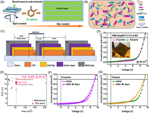
Moreover, Figure 5A shows the schematic diagram of spin to bar coated. A scheme that illustrates the carrier behaviors of the ternary blend is shown in Figure 5B, in which the homogeneity morphology and the superior carrier behaviors (efficient exciton generation/splitting efficiency) can be found. To verify the advantages of this ternary blend system for upscaling, we fabricated ternary devices with different active areas.
2.6 Photovoltaic properties of scalable sub-modules
Halogen-free solvent processing facilitates the development of scalable commercial sub-modules. As shown in Figure 5C, sub-modules (55 cm2) were fabricated by D-bar coating under ambient conditions (23 ± 3°C and RH 20% ~ 30%).24, 37, 40 The control device PM6:L8-BO sub-module (Figure S18) had a PCE of 13.40% and a Voc of 9.06 V, a Jsc of 2.45 mA/cm2, and an FF of 60.49%. Notably, PM6:NapBDT-C12:L8-BO sub-module had an impressive PCE of 14.69% (Figure 5D and Table 2) and significantly better Voc, Jsc, and FF values of 9.16 V, 2.46 mA/cm2, and 64.99%, respectively. To our knowledge, a PCE of 14.69% is the highest reported value for a halogen-free solvent-processed sub-module (Figure 5E; Table S7). This enhanced performance can be attributed to a more uniform homogeneous morphology. As shown in Figure S19, the UV–vis spectra of various sections of the ternary blend film remained relatively constant, which improved photovoltaic parameters. This result was further supported by a sub-module PCE of 14.58% when toluene was used as the solvent (Figure 5D). In addition, PM6:NapBDT-C12:L8-BO sub-modules had an excellent cell-to-module loss (PCElarge/PCEsmall) value of 0.78, which is one of the highest values reported for halogen-free solvent processed sub-modules,41 and supports the uniformity and pinhole-free nature of the active layer film, and resulting minimized small-area-to-module PCE loss.
| Active layera | Voc (V) | Jsc (mA/cm2) | FF (%) | PCEb (%) | PCElarge/PCEsmall |
|---|---|---|---|---|---|
| PM6:L8-BO | 9.06 (8.96 ± 0.10) | 2.45 (2.24 ± 0.24) | 60.49 (64.49 ± 0.4) | 13.40 (13.53 ± 0.17) | 0.74 |
| PM6:NapBDT-C12:L8-BO | 9.16 (9.04 ± 0.12) | 2.46 (2.32 ± 0.14) | 64.99 (64.69 ± 0.3) | 14.69 (14.57 ± 0.12) | 0.78 |
- a Processed using O-xylene.
- b Determined for an average of 7 sub-modules.
Device stability is another important factor, and thus, PM6:NapBDT-C12:L8-BO-based sub-module stability was tested under environmental conditions (23 ± 3°C and RH 25% ~ 30%). As shown in Figure 5F,G and Table S8, the sub-module retained >93% of its original PCE after storage for 90 days, indicating good morphological and chemical stability. These results suggest that NapBDT-C12 is an excellent choice for producing homogeneous and growth manipulation efficient halogen-free solvent-processed scalable sub-module devices.
3 CONCLUSION
In summary, we successfully report a robust guest donor polymer (NapBDT-C12), component for the fabrication of efficient small-area-to-sub-module OSC devices using a halogen-free solvent. Upon addition of carefully optimized amount of NapBDT-C12 was added into an optimized binary blend host (PM6:L8-BO) showed a remarkable improvement in the photovoltaic performance. It was found that great compatibility between PM6 and NapBDT-C12, facilitated the formation of cascade energy levels, favorable morphology, significantly greater charge extraction, balanced charge transport, and better device performance. Using this manipulation strategy, we achieved a reproducible and high PCEs (18.71% and 14.69%) for both small-area and scalable sub-module devices processed using O-xylene solvent. Overall, we presented a robust strategy of designing a donor polymer guest component benefits our understanding of active layer growth dynamics and furthers the industrial development of OSCs.
4 EXPERIMENTAL SECTION
Supporting Information contains experimental details and further characterization information.
AUTHOR CONTRIBUTION
Thavamani Gokulnath: Conceptualization, experimentation, methodology, validation, writing – original draft. Hyerin Kim: Formal analysis. Donghyun Song: Experimentation, methodology. Ho-Yeol Park: Methodology. Je-sung Jee: Formal analysis. Young Yong Kim: Experimentation, data curation. Jinhwan Yoon: Experimentation, data curation. Kakaraparthi Kranthiraja: Formal analysis, data curation, writing-review & editing. Sung-Ho Jin: Conceptualization, validation, project administration, supervision, writing – review & editing.
ACKNOWLEDGMENTS
This work was supported by the National Research Foundation (NRF-2018R1A5A1025594 and 2022R1A2C2091150) by the Ministry of Science, ICT of Korea.
CONFLICT OF INTEREST STATEMENT
The authors declare no conflict of interest.


