Novel Insights Into Load Current Control Using Power MOSFET
Funding: This work was supported by Viet Nam National University Ho Chi Minh City, TX2024-20b-01.
ABSTRACT
Power MOSFETs are critical in applications involving load current control, where system performance is significantly affected by their operating regions. This paper investigates the operational characteristics of power MOSFETs and proposes a novel approach for load current control based on their transconductance properties. By analyzing the relationship between MOSFET operating regions and load current dynamics, a control strategy that directly regulates the gate-source voltage to achieve precise current control is established. Furthermore, a gate driver circuit is designed to extend the controllable voltage range and enhance sensitivity to drain current variations. To improve current sensing accuracy, a methodology for designing a shunt resistor is introduced, leveraging the theoretical load curve of MOSFETs. Simulations using Simscape models and experimental validation confirm that the proposed method effectively extends the controllable voltage range of the drain current. Specifically, the voltage range can increase by up to 75% under load conditions compared to the absence of a shunt resistor, providing improved flexibility in current regulation. These findings offer novel insights into the use of power MOSFETs for load current control, with potential applications in digitally controlled power systems and motor drives.
1 Introduction
Load current control plays a crucial role in power electronics systems, particularly in the modern industrial landscape, where advancements in power electronic devices and automation technologies have led to increasing demand for precise and efficient current regulation. Accurate load current control not only ensures system efficiency, stability, and operational safety but also protects components from overcurrent conditions, reduces power losses, and extends device lifespan [1]. In applications such as electric motor control, power supplies, battery charging, and high-power drive systems, maintaining a stable load current is essential for optimizing performance [2-4]. Specifically, in DC motor control, the load current is directly proportional to torque; hence, precise current regulation improves system response and efficiency [5]. With the growing demand in fields such as electric vehicles, renewable energy, and embedded intelligent systems, effective load current control has become a fundamental requirement for improving operational performance and system reliability.
Over time, load current control has evolved from simple physical mechanisms to more complex control strategies that use power electronics and sophisticated control algorithms. Initially, load current regulation relied on passive components such as series resistors or variable resistors, where resistors limited current flow by dissipating excess energy as heat [6, 7]. While these methods were straightforward and easy to implement, they suffered from large power losses, reduced overall efficiency, and lacked precise control over current regulation. With the invention of power semiconductor devices, switching mechanisms like thyristors, bipolar junction transistors (BJTs), metal-oxide-semiconductor field-effect transistors (MOSFETs), and insulated-gate bipolar transistors (IGBTs) were introduced to enhance current control efficiency. In these, pulse-width modulation (PWM) became a widely adopted technique due to its ability to control average current without consuming a lot of power [8]. By rapidly switching between on and off states, PWM guarantees high efficiency [9]. However, a major limitation of PWM is its inability to directly regulate a continuous load current, as the current naturally oscillates between peak and minimum values within each switching cycle. This can be detrimental to applications requiring smooth and stable current flow [10]. Additionally, PWM causes undesired harmonic distortions and electromagnetic interference (EMI) in the system [11, 12].
Recent advancements in load current control have incorporated current sensors and feedback circuits to improve precision. These systems utilize shunt resistors, Rogowski coils, or Hall effect sensors to measure load current in real time and adjust the control output accordingly [13]. Integrating sensors with digital control algorithms significantly enhances accuracy and stability, especially in complex applications such as motor drives and high-power transmission systems. Additionally, the emergence of intelligent control technologies has introduced new approaches, including artificial intelligence (AI) and machine learning (ML), that enable real-time parameter optimization without the need for explicit mathematical models [14]. These algorithms improve performance and adaptability in dynamic load conditions. However, AI-based implementations remain limited due to high computational requirements and the need for extensive training data.
Beyond PWM, some current control architectures employ linear control techniques by regulating the conduction state of semiconductor devices. In certain applications, MOSFETs operate in either the linear or saturation region to regulate current flow similarly to an adjustable current source [15, 16]. This method provides smoother current control compared to PWM but presents several significant limitations. First, operating MOSFETs in the linear region results in higher power dissipation, negatively affecting system efficiency. Second, the control range within the linear region is inherently narrow, making precise current regulation challenging, particularly in applications requiring a wide dynamic range [17].
Furthermore, a key drawback of linear control is the nonlinear relationship between drain current and gate-source voltage in the saturation region, which complicates accurate current control. Additionally, thermal effects influence critical MOSFET parameters, such as threshold voltage, leading to deviations in control performance. Another significant challenge is that linear current control requires a very narrow gate voltage range to maintain MOSFET operation in the saturation region, making the system highly susceptible to noise and measurement errors.
Inspired by these challenges, this study investigates load current control using power MOSFETs, with a specific application to permanent magnet DC brushed motors, aiming to meet dynamic control requirements across various applications. Since the torque of a DC motor is directly proportional to the armature current, the drain current in a series-connected MOSFET can serve as a measurable indicator of torque production. This simplifies control implementation compared to complex algorithmic methods. Furthermore, this research provides valuable insights into MOSFET operating points, covering cutoff, saturation, and Ohmic regions, along with load characteristics. When operating in the saturation mode, the MOSFET functions as a variable resistor to achieve the desired drain current under gate voltage control, making it feasible for integration with digital controllers.
In summary, the main advantages of this study are: (1) Proposing a concept of current control for DC brushed motors using a power MOSFET operating in the saturation mode. This is beneficial for applications requiring simple torque control drives and provides a clear insight from theory to practice for beginners learning electric/electronic circuits; (2) Designing a gate driver to enhance the resolution of voltage-based current control, given the narrow voltage range to maintain the MOSFET in the saturated region; (3) Offering a design methodology for the shunt resistor to measure the drain current, setting this study apart from existing literature; and (4) Confirming the consistency of the findings through simulations supported by multi-physical domains and experimental test benches. With those contributions, the paper not only improves the MOSFET-based load control capacity but also develops a fundamental strategy that works well for power control systems requiring flexibility and deployment simplicity.
2 Theoretical Analysis
Essentially, the unidirectional current passing through a direct current (DC) brushed motor driven by an N-channel power MOSFET is depicted in Figure 1a, with its equivalent circuit model shown in Figure 1b. The performance of the DC brushed motor depends on the main power supply (V) and the operational point of the MOSFET, which is controlled by the gate-source voltage (V), and consequently, the controlled voltage (V). Although the gate input is known for its high impedance, a gate resistor is necessary to prevent overshoot current between the drain and source during switching. A larger gate resistor value increases switching time and heat generation. Conversely, small gate resistor is inadequate for reducing ringing, which may lead to damped oscillations. A well-chosen value in the range of 10–50 is suitable for this gate resistor. For practical current control applications, a shunt resistor is a well-established method to sense the drain current flowing through the MOSFET.
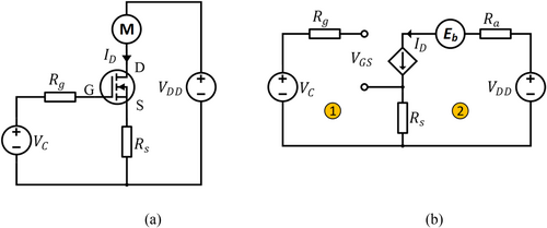

Figure 2 illustrates four load lines representing the load characteristics under full-load, no-load and with/without the shunt resistor The subscript denotes for no load operation of DC brushed motor, while signifies full-load operation. The superscript indicates the scenario without a shunt resistor, whereas represents the utilization of a shunt resistor. When the gate-source voltage is lower than its threshold voltage , the MOSFET operates in the cut-off region ( resulting in When increases to be greater than its threshold, say , the operating point of the MOSFET is at (saturation region), yielding the drain current . If the gate-source voltage is greater than a critical value , corresponding to and the operating point , such as , the MOSFET reaches the operating point (linear region) with the drain current For the maximum gate-source voltage , the MOSFET operates in the linear region with a drain-source voltage nearly zero and yields the drain current With the utilization of a shunt resistor, the drain current corresponding to yields a value of , which is lower than
For electrical current control applications using MOSFETs, it is expected that the drain current gradually increases as the controlled voltage is swept. However, it is proven that the drain current of MOSFETs dramatically increases in proportion to the square of the change in gate-source voltage in the saturation mode, while it only slightly increases in the linear mode. This prevents smooth current control through a load.
3 Case Study
A current control application using a Maxon DC brushed motor with the item code 133801, and an N-channel power MOSFET STB60NF10–1, is conducted to study the I-V characteristics of MOSFETs and develop a control circuit with suitable electronic components. The parameters of the DC motor obtained from the manufacturer's datasheet are specified in Table 1. It should be noted that these parameters concerning motor torque solely involve motor characteristics.
| Parameters | Value | Unit | Parameters | Value | Unit |
|---|---|---|---|---|---|
| Nominal voltage | 24 | V | Stall torque | 240 | mNm |
| No load speed | 9660 | rpm | Stall current | 10.3 | A |
| No load current | 37 | mA | Torque constant | 23.2 | mNm/A |
| Max. continuous torque | 28.4 | mNm | Speed constant | 412 | rpm/V |
| Max. continuous current | 1.46 | A | Rotor inertia | 10.3 | gcm2 |
| Nominal speed | 8330 | rpm | Speed/torque gradient | 41.2 | rpm/mNm |
| Armature inductance | 0.24 | mH | Armature resistance | 2.32 |
The motor torque can reach mN.m at full load while the angular velocity remains at rad/s. By using these data, one can calculate the damping coefficient corresponding to the case of full load, specifically (Nms/rad). Additionally, from the datasheet of STB60NF10–1, V, V, , A.
3.1 Theoretical Verification via Simulation Study
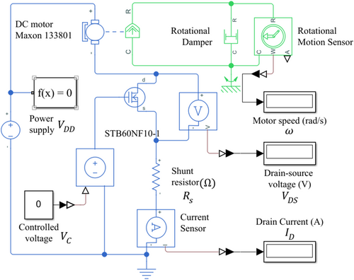
A Simscape model with electrical and mechanical domains was built in MATLAB to simulate the characteristics of MOSFETs driving the drain current flowing through the DC motor, as shown in Figure 3. The power supply is set to a fixed constant voltage of 24 V, while the controlled voltage can be adjusted by a constant block after each simulation iteration. The armature part of the DC motor is connected in series to the N-channel MOSFET, and a shunt resistor . The rotational mechanism of the DC motor is connected in parallel with a rotational damper. This damper acts as a damping coefficient , preventing the rotational motion of the combined motor shaft. The drain current, the drain-source voltage, and speed of combined motor shaft are measured by an ideal current sensor, ideal voltage sensor, and ideal rotational motion sensor, respectively, which do not affect the behavior of control circuits. The DC motor and the N-channel MOSFET in Simscape model capture the previously specified parameters, with the gate-source threshold voltage set to .
There are four simulation scenarios using the Simscape model, considering no load/full load and with/without shunt resistor. The controlled voltage is swept from to V with the incremental of 1 V, consistently for all iterations (Table 2). The shunt resistor and the damping coefficient (rotational damper) are set to zero for the first simulation iteration, with the results shown in Table 3.
| Mode | (rad/s) | |||
|---|---|---|---|---|
| 1 V | 24 V | Cut-off | 2.4 e−11 A | 1.9 e−5 |
| 2 V | 24 V | Cut-off | 2.4 e−11 A | 1.9 e−5 |
| 3 V | 24 V | Cut-off | 2.4 e−11 A | 1.9 e−5 |
| 4 V | 24 V | Cut-off | 2.4 e−11 A | 1.9 e−5 |
| 5 V | 10.66 mV | Linear | 36.98 mA | 1010 |
| 6 V | 5.31 mV | Linear | 36.99 mA | 1010 |
| 7 V | 3.54 mV | Linear | 36.99 mA | 1010 |
| 8 V | 2.65 mV | Linear | 36.99 mA | 1010 |
| 9 V | 2.13 mV | Linear | 36.99 mA | 1010 |
| 10 V | 1.77 mV | Linear | 36.99 mA | 1010 |
| Mode | (rad/s) | |||
|---|---|---|---|---|
| 1 V | 24 V | Cut-off | 2.4 e−11 A | 1.9 e−5 |
| 2 V | 24 V | Cut-off | 2.4 e−11 A | 1.9 e−5 |
| 3 V | 24 V | Cut-off | 2.4 e−11 A | 1.9 e−5 |
| 4 V | 24 V | Cut-off | 2.4 e−11 A | 1.9 e−5 |
| 5 V | 11.06 mV | Linear | 36.92 mA | 1010 |
| 6 V | 5.41 mV | Linear | 36.93 mA | 1010 |
| 7 V | 3.59 mV | Linear | 36.93 mA | 1010 |
| 8 V | 2.69 mV | Linear | 36.93 mA | 1010 |
| 9 V | 2.15 mV | Linear | 36.94 mA | 1010 |
| 10 V | 1.78 mV | Linear | 36.94 mA | 1010 |
It should be noted that when It can be seen that when is smaller or equal to , the MOSFET acts as an off switch, with the drain current nearly zero. The operating points of the MOSFETs for these iterations are in the cut-off region. As reaches V, the MOSFET conducts and operates in the linear region, resulting in a relatively small drain-source voltage mV and a no-load drain current of mA. With the change of from to V, the drain-source voltage decreases from to mV, while the drain current slightly changes by mA. It can conclude that the MOSFET transitions from the cut-off through the saturation to the linear region as the controlled voltage is in range of V.
Table 4 represents the simulation results of the MOSFET connected in series to the shunt resistor in driving the DC motor with no load. Compared to the previous scenario, the drain current is slightly smaller due to the presence of the shunt resistor. The larger the value of the shunt resistor, the smaller the drain current. The drain-source voltages of these two scenarios show insignificant differences because solely depends on as the MOSFET operates in the linear mode, regardless of the shunt resistor. Additionally, the MOSFET still transitions from the off-switch state to the on-switch state, ignoring the saturation duration, as the controlled voltage increases by 1 V from its threshold.
| Mode | (rad/s) | |||
|---|---|---|---|---|
| 1 V | 24 V | Cut-off | 2.4 e−11 A | 1.7 e−8 |
| 2 V | 24 V | Cut-off | 2.4 e−11 A | 1.7 e−8 |
| 3 V | 24 V | Cut-off | 2.4 e−11 A | 1.7 e−8 |
| 4 V | 24 V | Cut-off | 2.4 e−11 A | 1.7 e−8 |
| 5 V | 459 mV | Linear | 1.234 A | 872.5 |
| 6 V | 187.8 mV | Linear | 1.248 A | 882.6 |
| 7 V | 122.2 mV | Linear | 1.251 A | 885 |
| 8 V | 91.1 mV | Linear | 1.253 A | 886.2 |
| 9 V | 72.6 mV | Linear | 1.254 A | 886.8 |
| 10 V | 60.5 mV | Linear | 1.255 A | 887.3 |
When the rotational damper is set to a certain damping coefficient , it simulates the DC motor working with full load, preventing the acceleration of the combined motor shaft speed. The simulation results illustrate the characteristics of the MOSFET without a shunt resistor driving the DC motor with full load, as shown in Table 5. The drain current reaches the nominal current of the DC motor as the controlled voltage transitions from to V. This leads to an increase in the drain-source voltage, deviating from the no-load current. Once the MOSFET operates in the linear region, the drain current shows an insignificant increase of 21 mA when the controlled voltage is swept from to V.
| Mode | (rad/s) | |||
|---|---|---|---|---|
| 1 V | 24 V | Cut-off | 2.4 e−11 A | 1.7 e−8 |
| 2 V | 24 V | Cut-off | 2.4 e−11 A | 1.7 e−8 |
| 3 V | 24 V | Cut-off | 2.4 e−11 A | 1.7 e−8 |
| 4 V | 24 V | Cut-off | 2.4 e−11 A | 1.7 e−8 |
| 5 V | 14.42 V | Saturation | 0.477 A | 337.4 |
| 6 V | 651.1 mV | Linear | 1.163 A | 822.3 |
| 7 V | 198.2 mV | Linear | 1.185 A | 838.3 |
| 8 V | 124.1 mV | Linear | 1.189 A | 840.9 |
| 9 V | 90.8 mV | Linear | 1.191 A | 842 |
| 10 V | 71.8 mV | Linear | 1.191 A | 842.7 |
Table 6 represents the simulation results of the DC motor with full load driven by the MOSFET connected in series to the shunt resistor . It can be seen that the MOSFET transitions from the cut-off region to the saturation region as increases from to V, and it switches into the linear regime as reaches V. Additionally, it reveals that the drain current deviates by 714 mA when is in the range of V. There is a significant difference in the drain current between the presence and absence of the shunt resistor. It can be concluded that the slope in the characteristic line of the controlled voltage and the drain current decreases as the shunt resistor increases. However, this increase may cause overheating problems in the shunt resistor and prevent the upper limit of the maximum drain current.
| Step 1: Terminate AO-1 channel to set as zero; |
| Step 2: While!(Is detected): |
| Step 2.1: Increment with a small sufficient ; |
| Step 2.2: Acquire throught AI-2 channel; |
| Step 2.3: If : |
| is detected; |
| Set ; |
| Else |
| Repeat the step 2.1; |
| Step 3: Derive a desired current through AI-1 channel denoting as ; |
| Step 4: Obtain the actual current as ; |
| Step 5: Compute the current error as |
| Step 6: Modulate by a propotional—integral control algorithm using the current error with the assist of a saturation function. |
3.2 Design of Shunt Resistor
The previous simulation results showed that the MOSFET exhibits a linearized relationship between the controlled voltage and the drain current with the support of the shunt resistor. Leveraging this benefit, a driver circuit for DC brushed motor using power MOSFETs interconnected to a microcontroller to govern the load current should incorporate a shunt resistor to sense the drain current. However, the shunt resistor not only significantly affects the drain current but also may cause thermal issues. Therefore, its value must be accurately computed based on the specific application. First, the full load current of the DC motor () is determined to establish the basis for computation process. It is expected that the MOSFET operates in the saturation region (from to ) while keeping its drain current within the limit of the full-load current. The controlled voltage, deviating from the threshold gate-source voltage, making the MOSFET operate in the saturation region. Additionally, it should exploit the full-range of output voltage from the microcontroller's digital-analog-converter to enable high resolution of voltage–current control.
For specific parameter settings of A, , V, and V, the shunt resistor is computed according to the condition of Equation (20), yielding . Figure 4 illustrates simulation studies using the previously defined Simscape model, conducted with set as and , respectively. The relationship between the drain current and the controlled voltage for these four values of the shunt resistor are respectively represented in blue solid, dashed, dotted, and dot-dashed lines. The red lines show the relationship between the gate-source voltage and the controlled voltage, while the black lines depict the relationship between the drain-source voltage and the controlled voltage. It can be seen that when specifically 4 V, the MOSFET operates in the cut-off mode, resulting in no drain current. Consequently, the controlled voltage equals the gate-source voltage, and this behavior is consistent for all values of the shunt resistor.
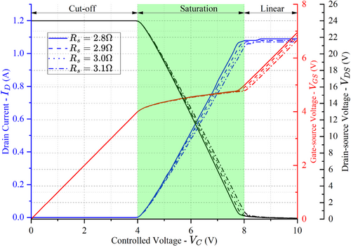
When exceeds V, the departure of the drain current from zero indicates that the MOSFET conducts. The drain current increases proportionally to the controlled voltage in the range of V to approximated V, depicting the saturation region. The larger the shunt resistor, the smaller the increment of the drain current with the increase in the controlled voltage. For the range of approximated to V in the controlled voltage, this voltage increases proportionally to the gate-source voltage due to a slight increase in drain current, indicating the linear region. It can be concluded that the saturation region of the MOSFET is expanded by using the shunt resistor for current sensing, enabling current control with a higher resolution of the controlled voltage. However, operating the MOSFET in the saturation region, which features a high voltage drop and high current flow, can lead to thermal issues for the MOSFET.
3.3 Design of Gate Driver
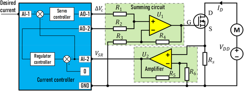
It should be noted that the MOSFET only conducts when exceeds its threshold . Therefore, the analog voltage produced by a microcontroller should be above the threshold gate-source voltage to enhance the resolution of the drain current with respect to the controlled voltage. However, the threshold gate-source voltage of each MOSFET varies, even within the same manufacturing lot. This study proposes synthesizing the controlled voltage for the MOSFET, which includes automatically adjusting the threshold gate-source voltage specific to each MOSFET, as well as the analog voltage produced by a microcontroller. This mechanism utilizes a non-inverting summing op-amp circuit with two inputs derived from the microcontroller's analog voltage outputs, as shown in Figure 5. The current controller consists of two sub-controllers: the servo controller, which tracks the desired current, and the regulator controller, which regulates the shunt current to zero, facilitating seamless operation and preventing dead band effects. The first channel analog output (AO-1) produces the analog voltage corresponding to modulated by the servo controller, while the second channel (AO-2) generates the threshold gate-source voltage (), specific to each MOSFET, to regulate the shunt current to zero. The servo controller drives the actual drain current, obtained by the second channel analog input (AI-2), to a desired current derived from the first channel analog input (AI-1). To this end, the drain current flowing through the shunt resistor yields a voltage drop that is elevated by a non-inverting amplifier with negative feedback provided by R5 and R6 then fed into the AI-2 channel.
| Datasheet | Tester device | Driver circuit | |
|---|---|---|---|
| MOSFET1 | |||
| MOSFET2 |
3.4 Experimental Testing
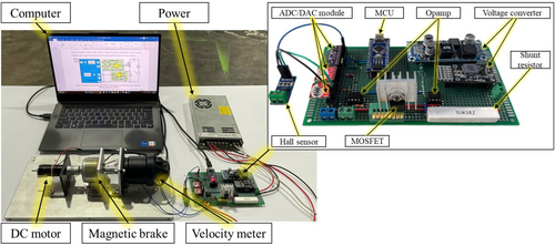
The experimental setup in Figure 6 is designed to study and evaluate the performance of the current control circuitry under various operational conditions. This test bench includes a Maxon 133,801 DC motor, a Magtrol HB-32-2 magnetic powder brake, and a Radio-Energie dynamo tachogenerator, enabling the creation of realistic test scenarios such as varying loads and controlling currents. The driver circuit is constructed according to the schematic shown in Figure 5. The power stage comprises an N-channel power MOSFET STB60NF10-1 connected in series with a cement shunt resistor. Two MCP4725 integrated circuits with 12-bit resolution act as buffer stages, converting two variable pulse width signals generated by an Atmega2560 microcontroller into two analog output channels, AO1 and AO2, spanning from 0 to 5 V. Meanwhile, two analog input channels, AI1 and AI2, are acquired by an ADS1115 analog-to-digital converter (ADC) with 16-bit resolution, interfacing with the microcontroller via the I2C protocol. Additionally, to address the challenges associated with current measurement without a shunt resistor, a Hall-effect-based linear current sensor ACS712 is employed to produce an analog voltage proportional to the drain current. This linear current sensor also facilitates the calibration of current measurements obtained from the voltage drop across the shunt resistor.
Firstly, the gate-source threshold voltage of MOSFETs used in the experimental test bench is determined using the driver circuit according to the strategy described in the pseudo-code. These experimental results are then compared to the direct measurements obtained using the FNIRSI LCR-P1 Multifunction Transistor Capacitor Tester. Table 7 indicates the gate-source threshold voltages of two MOSFETs, as per the manufacturer's datasheet, compared to the tester device and driver circuit measurements. The tester device indicates the gate-source threshold voltage as 3.43 and 3.14 V for MOSFET1 and MOSFET2, respectively, while the driver circuit gives 3.24 and 2.88 V. It is worth highlighting that the driver circuit shows the deviation of 5.5% and 8.2% compared to the tester device, and the deviation of 8% and 4% from the typical value.
Subsequently, these MOSFETs are used in experiments to control the current through the DC motor under various conditions of load in the presence and absence a shunt resistor. The experiment aims to demonstrate that the control range of is extended when a shunt resistor is employed.
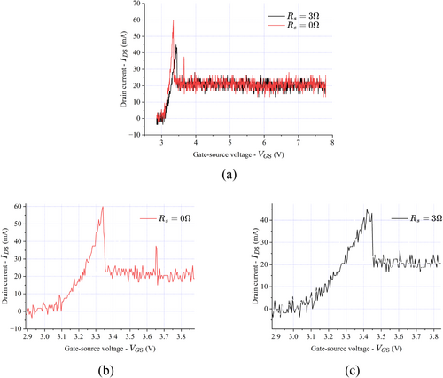
Figure 7a depicts the experimental result of the drain current through the DC motor under the test arrangement. The red curve represents the drain current without a shunt resistor (0 Ω), while that with a 3 Ω shunt resistor is expressed in black. During the experiments, the control voltage () is gradually increased while observing the corresponding current response () through the DC motor. During the startup phase, the motor requires a certain drain current to generate torque that overcomes the resistive torque caused by static friction. Once the motor runs, the drain current decreases to the steady state value, as shown in Figure 7b,c. Within this stage, the controllable range of the current is defined as , where is the maximum current required to sustain motor operation. It is clear to see that the inclusion of a 3 Ω shunt resistor provides a broader range of control voltage. This broader controllable range underscores the effectiveness of the shunt resistor in improving current regulation and operational stability of the DC motor under varying conditions.
Figures 8 and 9 illustrate the systems' behaviors under different load conditions, offering a broader perspective on the impact of load and shunt resistance () on the motors' electrical responses. During the startup phase, when no shunt resistor is presence (), the drain current () increases rapidly and exhibits pronounced oscillations at a lower range of the gate-source voltage () from approximately 4.3–4.7 V, as seen in Figures 8b and 9b. These oscillations are attributed to the absence of current-limiting resistance. In contrast, when is used, rises more gradually, and the oscillations are significantly suppressed, as observed in Figures 8c and 9c. It is worth noting that the occurrence of oscillations can be explained by examining the physical phenomena during motor startup. Initially, the motor is stationary, causing a large current to flow through the armature winding, due to the absence of substantial electromotive force (EMF) according to Faraday's Law. This drain current is generated to produce the torque that counteracts the resistive torque. It can be verified that a drain current of approximately 1.75 A is sufficient to make the motor run in both cases, with and without a shunt resistor. As the motor starts to rotate, the EMF increases, resulting in a rapid decrease in the drain current. Subsequently, it increases to overcome the load caused by the magnetic powder brake. By introducing , the inrush current is effectively controlled, minimizing the oscillatory behavior. This illustrates the critical role of the shunt resistor in mitigating instability and ensuring smooth operation during the motor's startup phase.
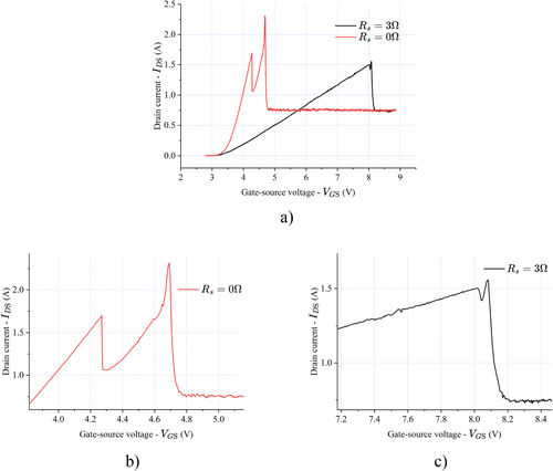
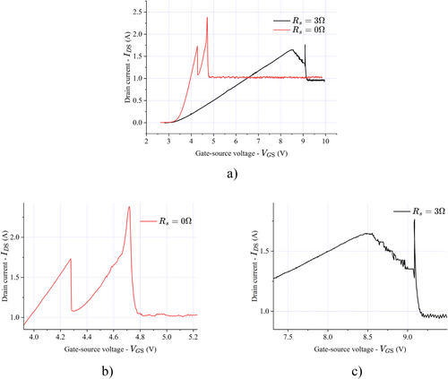
Table 8 illustrates that the controllable voltage range of is significantly extended when a shunt resistor is employed. This extension not only enhances the ability of the driver circuit to regulate current but also improves its sensitivity to small changes in current. Additionally, this improved sensitivity is particularly beneficial in applications requiring precise current control, as it enables more accurate adjustments and stabilization of the system's performance under dynamic conditions. The findings further validate the role of the shunt resistor in optimizing the overall control strategy.
| Controllable voltage range of | ||
|---|---|---|
| Load conditions | With a shunt resistor | Without a shunt resistor |
| No_load | ||
| Load_without brake | ||
| Load_with brake | ||
To validate the performance of the driver circuit, a current control for the DC motor using a Proportional-Integral (PI) algorithm was performed under varying conditions of reference drain current ( and changing loads. In the scenario involving control in drain current, illustrated in Figure 10a,b, the reference current () was adjusted according to a multi-level step function under constant load conditions. This experiment aimed to evaluate the accuracy of the proposed driver circuit in controlling the motor current. It is worth noting that the drain current rise sparkly (inrush current) to 1.0 A at 10-th second due to lack of a gate resistor to slow down the MOSFET's switching.
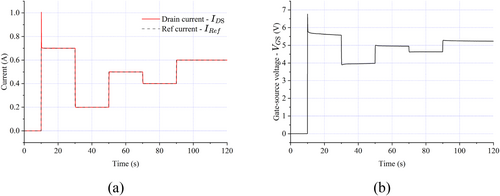
Using a multi-level step function to vary provides a robust framework for testing the system's responsiveness and stability across a wide range of operating points. The results demonstrate the circuit's capability to achieve precise current regulation, even when subjected to abrupt changes in reference current, thereby validating the effectiveness of the PI algorithm and the design's ability of the current control circuitry.
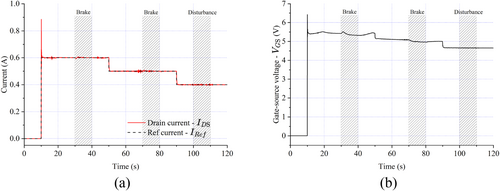
In the scenario involving load variations, as depicted in Figure 11a,b, the system was tested by activating the magnetic powder brake for a duration of 10 s while maintaining the control current at 600 and 500 mA, corresponding to the motor's dynamic operating states. Additionally, random disturbances were applied to the motor shaft for 10 s while the control current was set at 400 mA, sufficient to keep the motor in a stationary state. The experimental results demonstrated the capability of the proposed control circuit to maintain stable performance under various operating conditions. This included managing variations in control current and load as well as mitigating the impact of external disturbances.
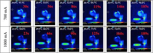
To verify the temperature development on the shunt resistor and the MOSFET over time, experiments were conducted to control the motor current at two levels: 700 mA and 1000 mA. During the test, the MOSFET was mounted with a heat sink to enhance heat dissipation, and the temperatures on the shunt resistor and the MOSFET were monitored using a Diacam2 Chauvin Arnoux C.A 1954 thermal camera.
Figure 12 presents thermal images captured at various time intervals, from 0 to 3 min. The results indicate that the MOSFET temperature increased rapidly during the initial phase and reached a saturation point of approximately at 700 mA and at 1000 mA. These values reflect a balance between the power dissipated by the MOSFET and the heat dissipation capacity of the system. Given that the operating temperature range of the MOSFET is , the measured temperatures confirm that the control circuit operates stably and within safe limits. This confirms that as long as the cooling system is designed efficiently, the current control circuitry can maintain long-term operation without overheating.
3.5 Extension of Proposed Method
The proposed method, originally developed for controlling load current in a single MOSFET configuration, can be extended to more complex circuit architectures, such as H-bridge circuits. This extension significantly enhances the applicability and flexibility of the method, allowing it to be adapted for various power electronics applications beyond DC motor control. By integrating the proposed approach into an H-bridge topology, the method can effectively manage current regulation in bidirectional motor drive systems, as well as in other applications requiring precise load current control.
To validate this extension, a simulation model was developed using Simscape, as illustrated in Figure 13, which simulates the MOSFET characteristics within an H-bridge configuration driving a DC motor. This simulation framework ensures that the proposed current control strategy remains effective even when applied to a more complex circuit structure. The results, presented in Table 9, confirm that the method operates successfully within the H-bridge circuit, demonstrating its potential for broader applications. Notably, the gate control voltage () required to achieve saturation, as previously analyzed in Tables 3–6, falls within the range of 4 V to 6 V, ensuring consistent operation within the desired region. These findings highlight that, depending on specific application requirements, the proposed method can be adapted for various purposes beyond DC motor control, extending its applicability to power regulation and current management systems.

| Rotation Direction | Mode | (rad/s) | |||||
|---|---|---|---|---|---|---|---|
| 4 V | 0 V | 10 V | 0 V | CW | Cut-off | ||
| 4.5 V | 0 V | 10 V | 0 V | CW | Saturation | 0.4362 | 390 |
| 5 V | 0 V | 10 V | 0 V | CW | Saturation | 0.9231 | 654 |
| 5.5 V | 0 V | 10 V | 0 V | CW | Linear | 0.9296 | 658.6 |
| 6 V | 0 V | 10 V | 0 V | CW | Linear | 0.9322 | 660.5 |
| 0 V | 10 V | 0 V | 4 V | CCW | Cut-off | ||
| 0 V | 10 V | 0 V | 4.5 V | CCW | Saturation | 0.1388 | −98.34 |
| 0 V | 10 V | 0 V | 5 V | CCW | Linear | 0.9146 | −648 |
| 0 V | 10 V | 0 V | 5.5 V | CCW | Linear | 0.9278 | −657.3 |
| 0 V | 10 V | 0 V | 6 V | CCW | Linear | 0.9314 | −659.9 |
4 Conclusion
This paper addresses the torque control problem of permanent magnet brushed direct current motors. Since the torque of a DC motor is naturally proportional to its armature current, this control challenge can be shifted into the domain of current control. Leveraging the transconductance of power semiconductors, the drain current of the MOSFET can be adjusted by the controlled voltage as it operates in the saturated region. Specifically, using a shunt resistor of sufficient value can enhance the sensitivity of the drain current concerning the controlled voltage. Furthermore, this study proposes a gate circuit to eliminate the deadband of the controlled voltage caused by the gate-source threshold voltage, thus enhancing the effective range of the controlled voltage to the drain current.
Experimental results confirmed that the controllable voltage range is significantly extended with the support of the gate driver when a shunt resistor is used. The controllable range can increase by 21% for the case of no load, 75% for the case with load and no brake, and 71.4% for the case with load and brake. Additionally, the armature current can seamlessly track a multi-level step function of the desired current with the support of the driver circuit under the control of the PI algorithm. These findings can benefit control practitioners in the domain of torque/current control for DC motors with a simple driver circuit. Future work will involve developing a multi-physic domain-based model that can monitor and estimate motor parameters in real time, serving as a digital twin for predicting the behavior of the control system.
Author Contributions
Huy Hung Nguyen: conceptual design, investigation, and writing. Quoc Minh Lam: coding and hardware implementation. Minh Nhat Huynh: data curation and Investigation. Trong Trung Nguyen: data acquisition and visualization. Van Tu Duong: validation, review, and editing. Tan Tien Nguyen: supervisor, analysis, and funding.
Acknowledgments
This research is funded by Vietnam National University Ho Chi Minh City (VNU-HCM) under grant number TX2024-20b-01. We acknowledge the support of time and facilities from the Key Laboratory of Digital Control and System Engineering (DCSELab), Ho Chi Minh City University of Technology (HCMUT), VNU-HCM for this study.
Disclosure
The authors have nothing to report.
Conflicts of Interest
The authors declare no conflicts of interest.
Open Research
Data Availability Statement
The data that support the findings of this study are available from the corresponding author upon reasonable request.


