High-Performance Inverted Perovskite Solar Cells with Sol–Gel-Processed Sliver-Doped NiOX Hole Transporting Layer
Abstract
Nickel oxide (NiOX) has been established as a highly efficient and stable hole-transporting layer (HTL) in perovskite solar cells (PSCs). However, existing deposition methods for NiOX have been restricted by high-vacuum processes and fail to address the energy level mismatch at the NiOX/perovskite interface, which has impeded the development of PSCs. Accordingly, we explored the application of NiOX as a hybrid HTL through a sol–gel process, where a NiOX film was pre-doped with Ag ions, forming a p/p+ homojunction in the NiOX-based inverted PSCs. This innovative approach offers two synergistic advantages, including the enlargement of the built-in electric field for facilitating charge separation, optimizing energy level alignment, and charge transfer efficiency at the interface between the perovskite and HTL. Incorporating this hybrid HTL featuring the p/p+ homojunction in the inverted PSCs resulted in a high-power conversion efficiency (PCE) of up to 19.25%, significantly narrowing the efficiency gap compared to traditional n-i-p devices. Furthermore, this innovative strategy for the HTL enhanced the environmental stability to 30 days, maintaining 90% of the initial efficiency.
1 Introduction
Employing metal halide perovskite materials is a promising route for converting sunlight into electricity due to their high absorption coefficient, extended diffusion distance, prolonged charge carrier life, and affordability.[1-6] The power conversion efficiency (PCE) of organic/inorganic hybrid perovskite solar cells (PSCs) has surpassed 25.8%, a remarkable improvement from 3.8%.[7] PSCs can typically divide into conventional (n-i-p) and inverted (p-i-n) structures based on the bottom layer type.[8, 9] Although n-i-p PSCs performed excellent efficiencies, inverted PSCs have also attracted worldwide attention with several advantages, such as a simple preparation process, low hysteresis, good compatibility with tandem solar cells, and potential applications in flexible devices.[10-12]
The hole transporting layer (HTL) is crucial while reviewing the advancement of high-performance inverted PSCs. The reported HTL can be broadly categorized into organic and inorganic materials. Organic HTLs, such as 2,2′,7′,7′-tetrakis(N,N-di-p-methoxyphenylamine)-9,9′-spirobifluorene (Spiro-MeOTAD), poly(3,4-ethylene dioxythiophene): poly(styrene sulfonate) (PEDOT: PSS), and poly(triarylamine) (PTAA), have shown impressive performance[13-15] but are prone to moisture absorption and liquefaction that can lead to degradation of PSCs.[16-19] In comparison to organic HTL, inorganic HTLs, such as copper thiocyanate,[20, 21] copper iodide,[22, 23] copper oxide,[24, 25] and nickel oxide (NiOX),[26-28] have several advantages, including good chemical stability, easy preparation, high light transmittance, and affordability. Among these materials, NiOX has received significant attention as HTL in inverted PSCs because of its appropriate work function (about 5.4 eV), wide band gap (>3.4 eV),[29-31] outstanding stability, and simple fabricating.[32] Nevertheless, the performance of NiOX-based PSCs generally has been affected by important issues. First, the energy level mismatch between NiOX and perovskite at their interface leads to an energy shift. Second, the low conductivity of NiOX leads to low charge extraction efficiency and increases the probability of recombination at the interface. Finally, the lattice mismatch between NiOX and perovskite affects the growth of the perovskite layer and reduces device stability. To address these issues, interface engineering through a metal doping strategy for optimizing the conductivity and hole transporting of the NiOX layer has been commonly used.[33] Single-element doping with Li,[34, 35] Ag,[36] Cu,[37-40] Cs,[41] and Co[42] and dual-element doping with Li-Ag[43] and Li-Cu[44] are commonly used. These reports have indicated that, under the metal doping process, the carrier mobility and concentration of NiOX can be aligned robustly.[45] However, the current doping strategy of NiOX HTLs is still far insufficient for PSCs. Introducing ion dopants to the NiOX lattice can result in significant lattice disorder and defects, decreasing charge carrier mobility and recombination.[46, 47] Hence, maintaining the balance between carrier concentration and mobility is crucial when doping semiconducting materials like NiOX.[48] For efficient PSCs, the NiOX-perovskite interface needs high mobility and conductivity. For example, Tan et al. utilized lithium doping to better match the band structure of NiOX to that of the perovskite. Additionally, the amino-functionalized polymer (PN4N) interfacial layer effectively reduces the density of interface defect states and trap-assisted recombination, resulting in an open-circuit voltage (VOC) of 1.14 V and an efficiency exceeding 20%.[35] Despite the optimized devices exhibiting appropriate energy levels and excellent defect passivation capabilities, the result of these strategies is primarily reflected in the increase of VOC, leaving the potential for enhancing fill factor (FF) by optimizing non-radiative recombination.[49]
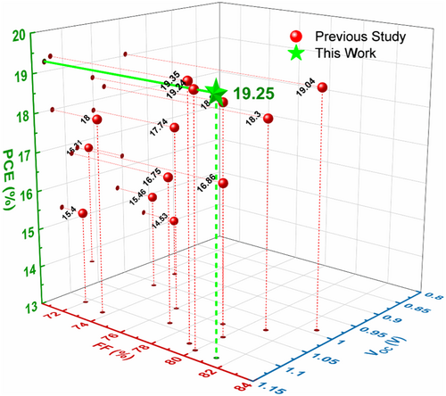
Herein, we demonstrated a hybrid silver doped-NiOX HTL executed homojunction to achieve high-performance inverted PSCs via a simple sol–gel solution process. The addition of Ag-NiOX increased the valence band maximum of the NiOX film from 5.40 to 5.46 eV. Furthermore, the hybrid NiOX film showed excellent driving force since the difference between Ag-NiOX and NiOX films' Ef was higher (0.09 eV) than that of the valence band bottom (0.06 eV). In contrast with previously reported doped NiOX-based HTL through sol–gel-processed for inverted PSCs, our work significantly improved all performance indicators of the inverted PSCs, as shown in Figure 1.[34, 36-39, 41-44, 50-54] Table S1, Supporting Information compares the parameters obtained in this work with previous reports. The optimized hybrid HTL greatly improves conductivity, carrier density, and ability to extract and transfer charge at the interface with the perovskite film.[55] The hybrid NiOX-based PSCs demonstrated a PCE of 19.25%, compared to the previous pristine NiOX-based PSCs' PCE of 16.2%. Additionally, the efficiency decay of hybrid NiOX-based PSCs was 90% lower than that of pristine NiOX-based PSCs (60%) under the 30-day environmental stability test. In conclusion, this innovative doping and homojunction introduction provides an effective approach for optimizing the interface engineering of the HTL in inverted PSCs, leading to significant improvement in various performance indicators.
2 Results and Discussion
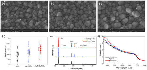
SEM imaging was used to examine the morphology of NiOX films before and after doping, as shown in Figure 2a–c. The films' morphology was uniform, continuous, and dense across all three types of films, with no cracks or holes observed. Small nanoparticles were visible on the surface, presumed to be NiOX, and likely formed due to solution contraction during annealing. SEM images of the various NiOX films indicated that their surface morphologies remained unchanged, implying that the introduction of Ag had no impact on the overall surface morphology of the films. As a result, uniform and dense NiOX films could be created.
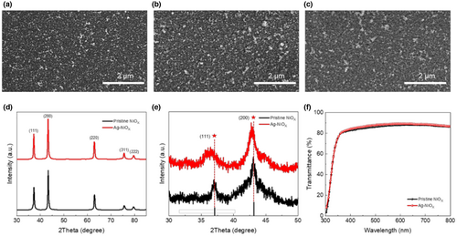
The synthesized NiOX and Ag-doped NiOX were first analyzed using XRD patterns to verify successful synthesis and identify any potential phase separation after doping. Figure 2d demonstrates that both NiOX and Ag-doped NiOX exhibited peaks at (111), (200), (220), (311), and (222) at angles of 37.09°, 43.1°, 62.8°, 75.6°, and 79.3°, respectively. Through comparison with the standard XRD card of NiOX (PDF#47–1049), indicating that NiOX was successfully synthesized through a sol–gel process. Without obvious peaks for silver components were found, and the diffraction of patterns of Ag-doped NiOX was similar to that of pristine NiOX, indicating Ag would not cause phase separation. However, as magnified patterns shown (Figure 2e), the diffraction peak shifts slightly towards smaller 2θ after Ag doped, suggesting the lattice was expended.[56] This is because the larger ionic diameter of Ag+ (1.15 Å) substituted the smaller ionic diameter of Ni2+ (0.69 Å), consistent with the Bragg equation: 2d sin θ = nλ.[57, 58] Additionally, all film samples exhibited high transmittance, with transmittance >80% in the wavelength range of 350–800 nm, as presented in Figure 2f. Interestingly, the transmittance level of the doped NiOX film was greater than that of the pure NiOX film due to the metal ion doping effect.[48]
The morphology of NiOX films is widely acknowledged to significantly influence perovskite film quality, hole transport, and electron-blocking effects. Figure S1, Supporting Information shows AFM images of different NiOX films, displaying smooth surfaces with densely clustered particles. The film types NiOX, Ag-doped NiOX, and Ag-doped NiOX/NiOX have root mean square (rms) values of 5.22, 5.50, and 5.89 nm. However, the difference in RMS values among the three films is not statistically significant, making it difficult to confirm that Ag doping alters the surface morphology and size of the NiOX film. Ag doping results in uniform, dense, and flat NiOX films that exhibit modified surface energy and crystallinity, potentially affecting both the growth and morphology of the perovskite film on the HTL, as revealed by XRD characterization. Control of the morphology of sol–gel-based prepared films can be challenging, but the study findings suggest that Ag doped in NiOX and hybrid treatment may substantially impact perovskite film quality, indicating the importance of exploring such treatments further.
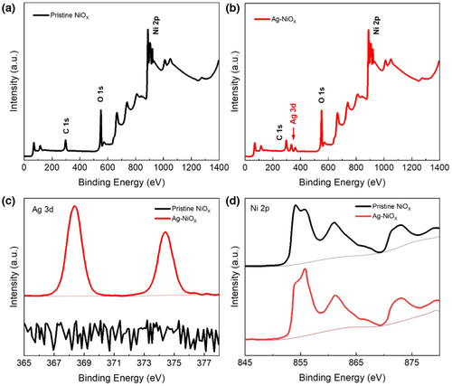
The chemical states of NiOX and Ag-doped NiOX were characterized using XPS analysis (Figure 3). Figure 3a,b present XPS data for NiOX and Ag-doped NiOX films, respectively. The emergence of a peak at 368 eV (Ag 3d5/2) and 374 eV (Ag 3d3/2) in the spectra confirms the successful doping of Ag in NiOX (Figure 3c), consistent with existing literature.[36, 45, 59] Figure 3d illustrates the Ni 2p XPS spectra of NiOX and Ag-doped NiOX. Using Lorentz-Gaussian functions (Figure S2, Supporting Information), we observed the appearance of two new peaks, including a main peak at 853 eV and a shoulder peak at 855 eV. These two peaks generally represent Ni2+ and Ni3+ peaks due to Ni2+.[60, 61] Notably, Ag doping led to a higher Ni3+/Ni2+ ratio in NiOX compared to undoped NiOX, thereby increasing the concentration of Ni vacancies. This, in turn, enhances the electrical conductivity of the film. These findings are consistent with the slight shift in XRD patterns and prior reports.[36, 43, 62]
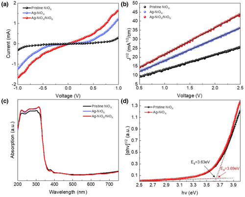
In this formula, represents the device area (4 mm2), and represents the thickness of the NiOX film (approximately 30 nm). We calculated the values of for various NiOX films with different concentrations of Ag doping, as shown in Table S2, Supporting Information. We observed that the σ0 of the NiOX films increased with increasing Ag doping concentration, but when the Ag doping concentration reached 4%, the conductivity tended to decrease. This decrease may be due to the low hole mobility caused by the high doping concentration. When the Ag doping concentration increased from 2% to 4%, more Ag+ ions replaced lattice Ni2+ sites, increasing the hole carrier concentration.
In this formula, represents the current density, is the vacuum permittivity, is the dielectric constant, and represent the hole mobility and thickness of different NiOX films, and represents the applied voltage. After fitting calculations, we observed that when the doping concentration reached 2%, μe reached a higher value of 2.1 × 10⁻² cm2 (V·S)−1. The values of μe were calculated for different concentrations of Ag doping, as shown in Table S2, Supporting Information. Similar to the explanation for the conductivity of different NiOX films, we observed that the carrier mobility of the film initially increased and then began to decrease when the doping concentration exceeded 2%. It is worth noting that the highest values for both hole conductivity (2.3 × 10⁻³ mS cm−1) and mobility (2.31 × 10⁻² cm2 (V·S)−1) are achieved in the NiOX hole transport layer with a hybrid structure, as shown in Table S3, Supporting Information. This improvement is attributed to forming a homojunction within the hybrid NiOX, which can further accelerate carrier mobility due to the built-in electric field.
The separation of photogenerated carriers and the resulting VOC of a solar cell device are primarily determined by the valence band offset between the hole transport layer and the perovskite layer. As such, it is essential to measure the work function. Figure 4c displays the UV–Vis of three different NiOX-based materials, while Figure 4d depicts the Tauc plots of pristine NiOX and Ag-doped NiOX films. These figures revealed that Ag doping increases the bandgap (Eg) of the film from 3.63 to 3.69 eV. Additionally, UPS analysis (Figure S3, Supporting Information) displays that the Fermi level (Ef) of NiOX and Ag-doped NiOX declines from 4.57 to 4.66 eV, leading to a higher VOC. Consequently, Ag doping reduced the valence band level of NiOX film from −5.40 to −5.46 eV, creating an improved energy level match between Ag-doped NiOX and the perovskite film, which boosted hole transport and reduced hole accumulation at the interface.[63] The band structure diagram in Figure 5a displays the calculated conduction band minimum (CBM) and valence band maximum (VBM), which determines the energy levels of the PSC.
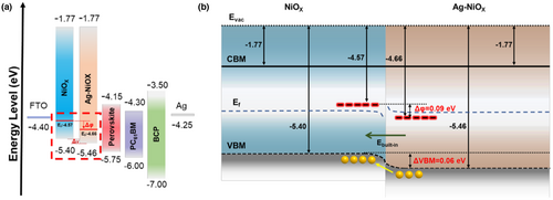
Figure 5b displays the energy bands of the functional layers relevant to the effect of the built-in electric field in hybrid NiOX on the device. Homojunction structures are well-known to improve carrier dynamics at interfaces. However, for both undoped and doped NiOX-based devices, charge separation driving forces are not outstanding, and there is no clear transport direction for photogenerated carriers, making undesirable electron–hole recombination more likely. Such recombination introduces non-radiative losses, which negatively impact device performance. The figure shows that the calculated VBM of Ag-NiOX is 0.06 eV lower than undoped NiOX. Nonetheless, when the hybrid NiOX structure is stable, the Fermi level of both doped and undoped NiOX is equivalent, inducing a band bending (Δφ = 0.09 eV) and forming a p/p+ homojunction structure. Consequently, from the surface to the bulk, the enhanced built-in electric field facilitates a favorable downward band bending in hybrid NiOX, providing a driving force for hole transport and promoting charge separation. Upon comparison with the energy level diagram of Ag-doped NiOX, it becomes evident that the energy level of Ag-doped NiOX is well-matched with the valence band energy level of the perovskite film, facilitating hole extraction and transport. This advantageous alignment of energy levels reduces charge recombination, ultimately leading to high-efficiency PSCs.
The morphology of the perovskite film is a key factor in determining the quality and performance of PSCs. To investigate the impact of Ag doping on the NiOX film, we used SEM to examine the surface morphology and size of perovskite films created on undoped NiOX, Ag-doped NiOX, and Ag-doped NiOX/NiOX films, as depicted in Figure 6a–c. The result shows that the perovskite films, with or without doping, adequately cover the HTL without any significant defects. However, the grain size of the perovskite film deposited on the doped NiOX-based layer was marginally larger than that of the undoped NiOX-based layer. The latter finding implied that the larger grain size of the perovskite film was beneficial for transferring both electrons and holes, while uniform and defect-free surface morphology favored the preparation of the upper electron transport layer.[18] Notably, the perovskite film is grown on the innovative hybrid NiOX film also had a larger grain size, supporting the view that this hybrid NiOX film exhibited a positive impact on perovskite film growth (Figure 6d). Furthermore, to investigate the crystallinity of the perovskite film, we performed XRD on the perovskite films grown on the three types of NiOX-based films mentioned earlier, as displayed in Figure 6e. The findings revealed that the perovskite film has significant peaks at 14.12°, 28.42°, and 31.78°, corresponding to its (110), (220), and (310) crystal planes. The perovskite films grown on Ag-doped NiOX and hybrid NiOX exhibited higher crystallinity than those grown on undoped Ag-doped NiOX, consistent with the SEM results. Meanwhile, the absorption spectra of the perovskite films grown on different NiOX-based films (Figure 6f) manifest strong light absorption in the ultraviolet to near-infrared wavelength range. Specifically, the perovskite film grown on Ag-doped NiOX film shows stronger absorption intensity, while the perovskite film grown on hybrid NiOX shows the most significant absorption intensity due to its higher crystallinity.[64] Thus, it is reasonable to conclude that incorporating Ag doping and improving the hybrid NiOX film result in a larger grain size of the perovskite film, which in turn enhances the UV-IR visible light absorption performance of the device.
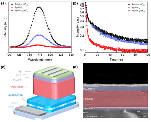
The fitted double exponential function of the curve is shown in Table S4, Supporting Information, with representing fast decay time, representing slow decay time, and representing the coefficient of decay amplitude. The observation shows that Ag doping increases the charge extraction ability of the perovskite film prepared on NiOX, resulting in a shorter carrier lifetime. Comparing the perovskite films on three different NiOX bases, the hybrid NiOX method generated the perovskite film with the shortest carrier lifetime and the strongest hole-extracting ability, indicating faster charge separation and transfer at the perovskite interface, minimizing the possibility of non-radiative recombination caused by defects.[67] Thus, achieving maximum improvement in the film.
To investigate the effect of Ag-doped NiOX and hybrid Ag-doped NiOX as HTLs on the performance of PSCs, inverted PSCs were fabricated with the structure FTO/three types of NiOX (30 nm)/Cs0.05 (FA0.83MA0.17)0.95 Pb(I0.83Br0.17)3 (450 nm)/PC61BM (70 nm)/BCP (6 nm)/Ag (50 nm). The PSCs' structure and cross-sectional SEM are depicted in Figure 7c,d. The optimal J–V curves of PSCs with different HTLs are shown in Figure 8a. Moreover, using hybrid NiOX as the HTL showed the highest short-circuit photocurrent density (JSC) (21.03 mA cm−2) and increased VOC, FF, and PCE. The increase in VOC (from 1.10 to 1.13 V) could be attributed to the increase in the valence band and the consequent increase in the built-in electric field, consistent with the results of UPS. Additionally, the device exhibiting hybrid NiOX as the HTL shows the best FF (76–81%) compared to the control group. This improvement could be attributed to the impact of the built-in electric field and the optimization of the HTL/perovskite film, which promotes charge transfer and extraction at the interface while inhibiting charge recombination. It is worth noting that using hybrid NiOX as the HTL resulted in the highest PCE (19.25%) among the inverted PSCs, which shows an 18.83% improvement compared with the PSC using undoped NiOX as the HTL. Table 1 summarizes the parameters of the PSCs using the three types of NiOX employed as HTLs.

| VOC (V) | JSC (mA cm−2) | FF (%) | PCE (%) | |
|---|---|---|---|---|
| Pristine NiOX | 1.10 | 19.32 | 76.35 | 16.20 |
| Ag- NiOX | 1.11 | 20.28 | 78.49 | 17.58 |
| Ag- NiOX/NiOX | 1.13 | 21.03 | 81.26 | 19.25 |
Figure 8b displays the IPCE and JSC curves for three NiOX-based PSCs. The JSC values obtained from the IPCE spectra match those from the J–V test. The IPCE curves of the three PSCs exhibit comparable trends, albeit with varying intensities. The hybrid NiOX-based PSC demonstrates the highest IPCE spectral intensity of 90% throughout the wavelength range, while Ag-doped NiOX-based PSC exhibits the second highest IPCE intensity. Furthermore, the hybrid NiOX-based PSCs display stronger IPCE intensity in the short and long wavelength range than undoped and Ag-doped NiOX-based PSCs due to the large built-in electric field within the innovative hybrid NiOX, which significantly reduces interface and bulk recombination. This, in turn, enhanced charge extraction and conversion rate at the Hybrid NiOX-Perovskite interface, providing suitable conditions for excellent crystallization of the perovskite layer.[68] Consequently, defects within the perovskite layer were effectively suppressed, thereby improving the IPCE of the PSC.
Figure 8c shows the hysteresis behavior of J–V curves of the three NiOX devices under different scan directions. The device parameters are listed in Table S5, Supporting Information. Undoped NiOX-based PSCs exhibit lower J–V curve overlap, unlike Ag-doped NiOX-based and hybrid NiOX-based PSCs. This is primarily due to the enhancement of the film conductivity, the reduction of the overall series resistance of the device after Ag-doping, and the introduction of the built-in electric field of hybrid NiOX. Therefore, the Ag-doping and hybrid NiOX-based PSCs exhibit higher J–V curve overlap, indicating greater stability and a lower tendency towards hysteresis.
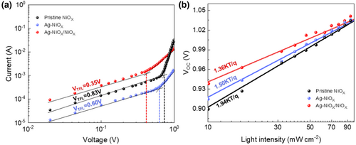
The stability of PSCs is an important benchmark for evaluating the effectiveness of optimization strategies and a decisive factor for achieving commercial production. To investigate the environmental stability of PSCs based on different architectures, the stability of inverted PSCs with pristine NiOX, Ag-doped NiOX, and hybrid NiOX as HTLs was compared at around 30% humidity and 25 °C. As shown in Figure S4, Supporting Information, the stability of the untreated NiOX-based PSC was the worst, with its efficiency dropping to only 70% of the initial value after 30 days. The Ag-doped NiOX-based PSC showed relatively stable performance but still exhibited some decay, with an efficiency of only 85% of the initial value. In contrast, the PSC based on hybrid NiOX as the HTL exhibited the highest stability, with an efficiency maintained at 90% of the initial value after 30 days. As shown in Figure S5, Supporting Information, light stability was observed. In contrast, after 260 h of exposure to a nitrogen environment, the PCE of a hybrid NiOX-based PSC remained steady at more than half of its initial efficiency. This indicates that this innovative strategy helps improve the interface layer between the HTL and perovskite, enhances the crystallinity of the perovskite film, and thus promotes the stability of PSCs.
3 Conclusions
We provide an innovative route for preparing a high-performance and stable inverted PSC based on Ag-doped NiOX/NiOX hybrid HTL via a sol–gel-based method. Compared with pristine NiOX, the Ag-doped NiOX film has higher conductivity, hole mobility, and a better-matched energy band structure with the perovskite layer. In addition, the homojunction in the Hybrid NiOX accelerates the extraction, transport, and reduction of carrier recombination at the interface. This innovative strategy effectively improves the crystallinity and morphology of the perovskite film. Compared with PSCs based on pristine NiOX (16.20%), the PCE of PSCs based on hybrid NiOX (19.25%) is 18.83% higher. Moreover, environmental stability has also been greatly improved. In summary, this innovative strategy of using Hybrid NiOX as the HTL in inverted PSCs provides an effective method for developing and commercializing high-efficiency and stable PSCs.
4 Experimental Section
Materials
Ethanolamine (C2H7NO, 99.5%), dimethyl sulfoxide (DMSO), N,N-dimethylformamide (DMF, 99.99%), γ-butyrolactone (GBL), N-methyl-2-pyrrolidone (NMP) and chlorobenzene (CB) was purchased from Alfa Aesar. Nickel nitrate hexahydrate (Ni(NO3)2·6H2O, 99.8%), silver nitrate (AgNO3, 99.9%), ethanol (C2H6O, 95.0%), and isopropyl alcohol (C3H8O, 99.7%) were purchased from Sigma-Aldrich. Lead iodide (PbI2, 99.99%), cesium iodide (CsI, 99.99%), lead bromide (PbBr2, 99.99%), methylammonium bromide (MABr), formamidine (FAI), bathocuproine (BCP), and phenyl-C61-butyric acid methyl ester ([6,6]-PC61BM, >99% purity) were purchased from Xi'an Polymer Light Technology Corporation, respectively.
Preparation of hole transporting layers
In order to prepare the NiOX precursor solution, Ni(NO3)2·6H2O (125 mg) was dissolved in 5 mL of isopropanol, followed by the addition of ethanolamine (with a Ni2+:C2H7NO molar ratio of 1:1). The solution was uniformly stirred at 50 °C and 500 rpm until completely dissolved to obtain a homogeneous and dispersed NiOX precursor solution. Different atomic ratios of AgNO3 (with Ag:Ni ratios of 1%, 2%, and 4%) were added to the NiOX precursor solution according to the specified proportions. These precursor solutions with different Ag-doped NiOx were diluted to a 50% concentration with deionized water and stirred uniformly at 50 °C and 500 rpm until completely dissolved.
To ensure consistent experimental results, a diluted precursor solution (50%) was first spin-coated onto a processed FTO substrate as the first layer (4000 rpm, 40 s), after which the substrate was dried at 100 °C for 10 min. The undiluted precursor solution was then spin-coated onto the substrate as the second layer, using the same spin-coating method. The resulting film was annealed at 350 °C for 60 min and transferred to a nitrogen-filled glove box. This same method was used to prepare the Ag-doped NiOX/NiOX hybrid film.
Fabrication of perovskite solar cells
FAI, PbI2, MABr, and PbBr2 (1:1, 1:0, 2:0.22 M ratio) were stirred in a DMF and DMSO mixture in a dry gas environment NMP (16:4:1) to prepare the perovskite active layer. DMSO solution with CsI (volume ratio 5:95) was added and placed in the first mixed solution at 60 °C for around 2 h. Next, the mixed perovskite precursor solution was spin-coated on the NiOX layer with a low-speed spinning at 1000 rpm for 10 s, followed by a high-speed spinning at 6500 rpm for 20 s. At the 25th second, chlorobenzene antisolvent was sprayed on substrates. The substrates were then annealed for 1 h at 100 °C. Then, a solution of PC61BM in chlorobenzene is prepared with a concentration of 2 wt% and stirred at room temperature for 1 h. The resulting mixture is filtered, and the PC61BM/chlorobenzene solution is spin-coated onto the perovskite film. The spin-coating process is performed twice: first at 1000 rpm for 5 s and then at 2500 rpm for 30 s. The substrate is annealed at 90 °C for 10 min on a hot plate after the spin-coating. Once the substrate has cooled, a thin layer of BCP is formed as a hole-blocking layer by dynamically spin-coating a BCP methanol-saturated solution onto the PC61BM substrate. The BCP is spin-coated at a rate of 1000 rpm for 5 s and 6000 rpm for 30 s, resulting in a thickness of 6 nm. Finally, a 50 nm-thick silver electrode is deposited onto the BCP layer through thermal evaporation in a vacuum with a pressure below 1 × 10⁻⁴ pa to form the back contact electrode.
Instruments
To analyze the X-ray diffraction (XRD) patterns, the Shimadzu XRD-7000 diffractometer with Cu Kα radiation was used. The Hitachi SU8220 was employed to observe the cells' surface morphology and cross-sectional thickness through atomic force microscopy (AFM) and scanning electron microscopy (SEM). Energy spectrum analysis of the materials was conducted through X-ray photoelectron spectroscopy (XPS) and ultraviolet photoelectron spectroscopy (UPS) using the ThermoFisher ESCALAB 250Xi spectrometer. To characterize the photoluminescence intensity and analyze the carrier lifetime of the thin film materials, the steady-state photoluminescence spectra (PL) and the transient photoluminescence spectra (TRPL) were obtained using the Edinburgh FS5 and FLS980 spectrometers, respectively. The devices' monochromatic light photoconversion efficiency (IPCE) was characterized using Newport Technology Company. The Varian Cary 300 UV–Vis spectrophotometer was utilized to measure the absorbance of the perovskite films. The PSCs' photovoltaic performance was analyzed by measuring J–V curves using a Keithley 2400 system and a 100 mW cm−2 AM 1.5 G standard Newport sun simulator.
Acknowledgements
This research was funded in part by the National Natural Science Foundation of China (62204210), the Natural Science Foundation of Jiangsu Province (BK20220284), the Natural Science Foundation of the Higher Education Institutions of Jiangsu Province (22KJB510013), the Natural Science Foundation of the Jiangsu Higher Education Institutions of China Program (19KJB510059), the Suzhou Science and Technology Development Planning Project: Key Industrial Technology Innovation (SYG201924), University Research Development Fund (RDF-17-01-13), and the Key Program Special Fund in XJTLU (KSF-T-03, KSF-A-07). This work was partially supported by the XJTLU AI University Research Centre and Jiangsu (Provincial) Data Science and Cognitive Computational Engineering Research Centre at XJTLU.
Conflict of Interest
The authors declare no conflict of interest.


