Atomic Level Insights into Metal Halide Perovskite Materials by Scanning Tunneling Microscopy and Spectroscopy
Abstract
Metal halide perovskite materials (MHPMs) have attracted significant attention because of their superior optoelectronic properties and versatile applications. The power conversion efficiency of MHPM solar cells (PSCs) has skyrocketed to 25.5 %. Although the performance of PSCs is already competitive, several important challenges still need to be solved to realize commercial applications. A thorough understanding of surface atomic structures and structure–property relationships is at the heart of these remaining issues. Scanning tunneling microscopy (STM) and spectroscopy (STS) can be used to characterize the surface properties of MHPMs, which can offer crucial insights into MHPMs at the atomic scale. This Review summarizes recent progress in STM and STS studies on MHPMs, with a focus on the surface properties. We provide understanding from the comparative perspective of several different MHPMs. We also highlight a series of novel phenomena observed by STM and STS. Finally, we outline a few research topics of primary importance for future studies.
1 Introduction
Early studies on metal halide perovskite materials (MHPMs) can be dated back to 1893.1 However, interest in the perovskite materials was still rather limited at that time. It was only in 2009 that MHPMs were first used as a photosensitizer material in dye-sensitized solar cells2 and began to attract the attention of the scientific community. MHPMs have a perovskite crystal structure with a stoichiometry of ABX3. The crystal structure consists of a 12-fold coordinated A cation occupying the site in the middle of the cube, which is surrounded by 8 corner-sharing [BX6]4− octahedra. The possible selection of A, B, and X site ions are governed by the Goldschmidt tolerance factor,3 which is an empirical rule for predicting the stability and lattice distortion derived from the close-packing of spherical hard ions. In general terms, the A-site is typically occupied by an organic or inorganic monovalent cation, such as CH3NH3+ (MA+), CH(NH2)2+ (FA+), Cs+, or a mixture of these cations; the B-site is occupied by a divalent metal cation, such as Pb2+, Sn2+, Ge2+, or a mixture of these cations; the X-site is occupied by a monovalent halide anion, such as I−, Br−, Cl−, or a mixture of these anions.4 As a consequence of their excellent properties, MHPMs have emerged as a class of semiconductors with a broad range of applications, such as photovoltaics,4a, 4d, 4e, 5 photodetectors,4j, 6 light-emitting diodes,7 and lasers.8 Recently, the power conversion efficiency (PCE) of PSCs has skyrocketed from the initial 3.81 % to 25.5 %, which is approaching the record of crystalline silicon solar cells (26.1 %).9 Although the performance of PSCs is already competitive, several important challenges still need to be solved to realize commercial applications, such as inadequate long-term stability and reproducibility,4i, 10 upscalable fabrication,11 and potential concerns about toxic lead leakage during operation.12 A thorough understanding of surface atomic structures and structure–property relationships is at the heart of these remaining issues.13 The chemistry and physics at the surfaces and interfaces in the complex architecture of PSCs have a profound impact on device performance (in terms of both PCE and stability). Although research on device applications of MHPMs has reached an impressive level, a fundamental understanding of this interesting class of materials is currently somewhat lagging behind, in particular regarding atomic-level insights into the surface and interface properties and their influence on device stability and performance.
The morphologies and compositions of MHPMs are often characterized using techniques such as X-ray diffraction (XRD), scanning electron microscopy (SEM), and transmission electron microscopy (TEM). Unfortunately, these techniques either lack atomic-level spatial resolution in real space or may cause severe damage to the MHPMs as a result of high-energy electron bombardment.14 Scanning tunneling microscopy (STM), which is based on the quantum mechanical effect of electron tunneling, is a powerful tool that can be used to characterize the surface topographic and electronic properties of specimens with atomic resolution in real space. As a metallic STM tip approaches a sample surface to within a distance of a few angstroms, the tip and sample wave functions overlap, and an electron has a non-zero probability to tunnel through the barrier. If a small bias voltage is applied, a tunneling current (typically nanoamperes) is generated between the tip and the sample surface. This tunneling current is a function of the height of the tip relative to the surface and the local density of states at the sample surface. One of the advantages of STM is that it usually does not cause damage to the sample because of the negligible tunneling current and nonphysical contact. As a result of its unique operation principles, STM shows powerful capabilities in many aspects. For example, STM can probe the topography of the surface and interface with atomic resolution. It also allows in situ real-time monitoring and characterization of material growth and evolution processes, surface dynamics, and surface chemistry. Scanning tunneling spectroscopy can precisely reveal the electronic structures of the surface at the atomic scale. Furthermore, STM can be combined with many other ultrahigh vacuum (UHV) techniques to provide comprehensive characterization of the sample surface. Compared with transmission electron microscopy (another powerful technique with the capability of atomic-resolution imaging), STM experiments can be considered non-invasive and the sample preparation is relatively straightforward. However, STM requires an atomically smooth and conductive surface and a sharp metallic tip. Although STM can offer crucial insights into the fundamental understanding of materials ultimately at the atomic scale,15 STM studies on perovskite materials are still relatively rare, presumably because of the technical difficulty in obtaining an immaculate and atomically flat sample surface.13a, 16 Recent findings indicate that the surface trap states in the perovskite layer can strongly influence the performance of the solar cell devices;7b, 17 however, the chemical and physical properties of atomic-scale defects and surface and interface properties are not well-understood. The investigation of surface phase transitions, surface defect dynamics, ion migration, and halide-substitution of MHPMs is still in its infancy.
In this Review, we first summarize the methods to prepare high-quality MHPMs for STM characterization. We then elucidate the basic properties of perovskite sample surfaces, including atomic-scale topography, surface electronic properties, surface phase transitions, surface defect dynamics, halide substitution, enhanced stability, and interfacial structures. Finally, by considering the impact of the surface and interface on device performance, we propose a few future research directions for STM studies on metal halide perovskites.
2 Sample Preparation
An atomically flat surface with reasonable conductivity is key to successful STM studies; therefore, the preparation of MHPMs is the first crucial step. To achieve STM characterization, considerable efforts have been devoted to the development of different approaches to prepare or synthesize high-quality perovskite thin films.18 These approaches can be mainly classified as “cleavage” and “deposition”. The cleavage method applies a steady force to precisely cleave the bulk crystal to yield a fresh crystal plane; the deposition method is based on the interaction of atoms or molecules with the substrate to form high-quality thin films on the surface by sublimating the precursors under vacuum.
2.1 Vacuum Cleavage
Mechanical cleavage is commonly used to prepare and study a variety of single-crystalline samples, including inorganic semiconductors19 and two-dimensional (2D) layered materials.20 However, the tetragonal/cubic structure of MHPMs does not have an easily cleavable crystal plane.21 Even though cleavage is nontrivial for MHPMs, several studies have been reported to overcome this barrier.18c-18e Qi and co-workers succeeded in cleaving MAPbBr3 single crystals with a remaining thickness of about 1–2 mm.18e A single crystal of MAPbBr3 was mounted on a sample holder and cleaved with a scalpel parallel to one of the facets of the crystal inside the UHV chamber (Figure 1 a). For some particular samples, such as Sr3Ru2O7 and Sr2RuO4 oxide-type perovskites, the cleavage process does not generate intrinsic defects, which is explained by the high formation energies of 4.19 eV and 3.81 eV for the Sr and O vacancies, respectively.22 As a comparison, the formation energies for the Br and MA vacancies in MAPbBr3 and the I and MA vacancies in MAPbI3 are relatively low in halide perovskites (Table 1), as determined by experimental and theoretical studies on halide perovskite surfaces.18e, 18f, 22, 23 In addition, the observed defects on as-cleaved surfaces may be caused by the bulk impurities.22, 24 After a period of weeks under UHV and dark conditions, the fresh surface of MAPbBr3 degrades and converts into PbBr2.18c In addition, the MAPbBr3 perovskite possesses a stable cubic phase at room temperature (RT) and the orthorhombic phase at a temperature below 144.5 K.25 The step height was determined to be (6.0±0.6) Å for the cubic and (5.3±0.4) Å for the orthorhombic phases.18c, 18e The main reason for choosing bulk MAPbBr3 single crystals as the sample is that they are easier to prepare compared to other MHPMs because of their relatively large crystal size and high stability.18d In general, the vacuum cleavage process is nontrivial, but this method provides a feasible strategy to expose the clean interface and study the nature of the surface properties of MHPMs.
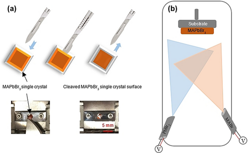
Illustration of sample preparation methods for STM. a) Vacuum cleaving of a MAPbBr3 single crystal. Adapted from Ref. 18e with permission. Copyright 2015 American Chemical Society. b) The dual-source vapor deposition set-up for MAPbBr3 films. Adapted from Ref. 18h with permission. Copyright 2014 The Royal Society of Chemistry.
MAPbI3 |
|
MAPbBr3 |
|
Sr2RuO4 |
|||||
|---|---|---|---|---|---|---|---|---|---|
VI [eV] |
VMA [eV] |
VMAI [eV] |
|
VBr [eV] |
VMA [eV] |
VMABr [eV] |
|
VSr [eV] |
VO [eV] |
0.08 [23a] |
0.16 [23a] |
0.23 [23b] |
|
2.39 [23f] |
3.32 [23f] |
1.96 [23f] |
|
4.19 [22] |
3.81 [22] |
0.29–0.87 [23c] |
−0.02–1.06 [23c] |
0.08 [23d] |
|
– |
– |
1.94 [18f] |
|
– |
– |
1.85 [23e] |
1.94 [23e] |
– |
|
– |
– |
– |
|
– |
– |
- [a] VX represents an “X” vacancy defect.
2.2 Vacuum Vapor Deposition
The vacuum vapor deposition method is a suitable technique for growing thin films, and has three advantages. Firstly, it is performed under a vacuum, so as-grown thin films have a high purity. Secondly, the films are grown at a controllable deposition rate, which is beneficial to ensure uniformity of the thin-film properties. Thirdly, it usually leads to a smooth surface. In general, an effective deposition process only occurs in a thermodynamically non-equilibrium state,26 which is strongly dependent on the free surface energy of the substrate and the adatoms, as well as the interfacial energy between them.27 In 2013, Snaith and co-workers succeeded in growing uniform flat and thin MAPbI3−xClx films with a thickness of approximately 330 nm on top of a glass surface coated by compact TiO2-coated fluorine-doped tin oxide (FTO) by using the dual-source co-evaporation method at 10−5 mbar.18g Two crucibles were loaded separately with MAI and PbCl2. The MAI source was then heated to about 120 °C, and PbCl2 was heated to about 325 °C.18g
Qi and co-workers focused on the preparation of MAPbX3 (X=Br or I) based perovskite thin films by dual-source co-evaporation in an UHV environment.18f, 18h-18k In the case of MAPbBr3, MABr and PbBr2 were evaporated at 361 and 498 K, respectively, for 10 min, while the clean Au(111) substrate was kept at 130 K during deposition to ensure the adhesion of the MABr molecules. The sample was then post-annealed at room temperature for 3 h. For MAPbI3, the MAI and PbI2 molecules were evaporated at 378 and 513 K, respectively, for 5 min, while the clean Au(111) substrate was kept at 130 K, and then the sample was post-annealed at room temperature over a period of approximately 120–180 min.18j, 18k Figure 1 b shows an illustration of a set-up for dual-source thermal evaporation deposition. By adjusting the evaporation time, MAPbBr3 perovskite thin films with different thicknesses could be prepared. Zhong and co-workers prepared MAPbI3 thin films on a Au(111) surface by co-deposition of MAI and PbI2 under UHV conditions.18m, 18n The height of the step edge of the MAPbI3 sheets is about 6.3 Å, which is half of the lattice constant of the orthorhombic MAPbI3 along the c axis, which indicates that these sheets consist of a monolayer thickness with an atomically smooth surface.28 As the deposition time was increased, a multilayer MAPbI3 film was obtained with a final nominal thickness of 10.8 monolayers on top of the substrate.18n This layer-by-layer growth method with well-defined surfaces allows precise elucidation of the structure–property relationships and is of crucial importance for the further development of MHPM solar cells. CsPbI3 and mixed halide perovskites such as MAPbBr3−yIy, MAPbBr3−zClz, and MAPbI3−xClx can also be fabricated by the vacuum deposition method.18i, 18j, 18o The CsPbBr3 perovskite films could also be prepared by using the single-source evaporation method.18r Different molar ratios of CsBr and PbBr2 powders were mixed and pressed into tablets as precursors. The TiO2-coated FTO-coated glass substrate was maintained at 300 °C, and simultaneously rotated during the deposition to obtain good homogeneity of the CsPbBr3 thin films. Triple-cation Cs0.5FA0.4MA0.1Pb(I0.83Br0.17)3 perovskite films were grown on the tin-doped indium oxide (ITO) coated glass substrate by using simultaneous multiple-source thermal evaporation, where the precursors were kept at about 425 °C for CsBr, 100 °C for MAI, 165 °C for FAI, and 295 °C for PbI2.29 Incorporation of inorganic Cs+ into MHPMs for the formation of multiple cation configurations is a common strategy to improve the performance, with better reproducibility and stability as well as higher efficiencies.10a, 30 The vacuum vapor deposition method could provide highly controllable thin perovskite films with a high quality, uniform morphology, and possibly reduced impurities and defects.
3 Characterization by STM-Based Techniques
3.1 Atomic-Scale Characterization of Various Metal Halide Perovskite Materials
The surface structures of MHPMs have been modeled by theoretical computations, and the surface reconstructions are usually found to originate from the instability of the surface layer as a result of perpendicular macroscopic polarization.31 Typically, the polar surface would be compensated by the surface reconstruction, which thus results in depolarization and the formation of the final stabilized layer. STM can be employed to determine the surface structures with high spatial resolution, which provides valuable insights into the fundamental understanding of perovskite materials.
3.1.1 MAPbBr3
Qi and co-workers successfully achieved the first atomic-level STM imaging of a vacuum-cleaved MAPbBr3 single-crystal surface.18e Since the STM measurements were performed at 4.5 K, the cleaved crystal exhibited an orthorhombic structure, and the lattice constant was calculated to be 7.87×12.02×8.79 Å3.32 A flat and smooth MAPbBr3 terrace was observed with a step height of half of the unit cell of MAPbBr3. High-resolution STM images showed the superlattice structure had two types of surface reconstruction configurations. As shown in Figure 2 a,b, bright protrusions could be distinguished in zigzag and dimer patterns. Both patterns co-existed in certain areas of the surfaces (Figure 2 c), which corresponded to the MABr-terminated surface based on first-principles density functional theory (DFT) calculations. Moreover, the PbBr-terminated (001) surface was also observed by STM, with a 2×2-like rectangular pattern (Figure 2 d).18d The STM measurements indicated that a few small areas were covered by the zigzag structure and that the prevalent structure is the dimer structure, which covered the majority of the surface.18d, 18f, 18i In addition, the dominant dimer structures tended to take <110> as the preferential directions. In contrast, the zigzag structures were formed by zigzag rows of Br anions aligned preferably along the [100] direction.18d With the support of DFT calculations, the bright protrusions were assigned to Br anions at the corner of the PbBr6 octahedra in the case of the MABr-terminated (001) surface of the orthorhombic crystal. These two distinct types of surface structures could be interpreted as two different in-plane orientation configurations of the MA cations. As presented in Figure 2 e,f, the zigzag structure was associated with a perpendicular arrangement of the MA cations, which resulted in a non-zero net dipole moment, while the dimer structure was associated with an antiparallel arrangement of the MA cations with a zero net dipole moment within the plane of the surface. The simulated STM images (Figure 2 e,f) were in good agreement with the experimental STM images (Figure 2 a,b). As a consequence of the strong electrostatic interaction between the MA cations and Br anions, reorientation of the MA cations within the plane of the surface would allow the Br anions to relax to another lower energy state, which might alter the position of the Br lattice. This is consistent with the results measured by the line profiles (Figure 2 g). A reorientation event was observed in the same row and this phenomenon is discussed in more detail in Section 3.3. In addition to the observed Br anions, the MA cations could be imaged with a reduced sample bias voltage (i.e. corresponding to a smaller tip–sample distance; see Figure 2 h), which showed additional protrusions corresponding to the MA cations, consistent with the calculation results (Figure 2 i).
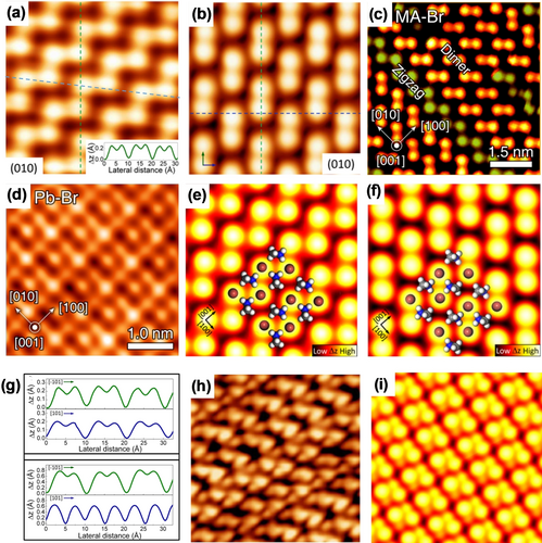
Atomic-scale characterization of the MAPbBr3 perovskite (001) surface. a) High-resolution STM image of a zigzag surface structure (31×31 Å2, U=−5 V, and I=0.1 nA). b) High-resolution STM image of the dimer surface structure (31×31 Å2, U=−9 V, and I=0.1 nA). Panels (a,b) are reprinted from Ref. 18e with permission. Copyright 2015 American Chemical Society. c) The two surface structures co-existing on the same terrace (U=−5.5 V and I=0.2 nA). d) High-resolution STM image of the PbBr-terminated (001) surface (U=−5.5 V and I=0.2 nA). Panels (c,d) are reprinted from Ref. 18d with permission. Copyright 2019 American Chemical Society. e,f) Simulated STM images of the zigzag and dimer structures. The Br and MA ions are overlaid. g) Line profiles along the dashed lines in (a) and (b) for the two different observed zigzag (top) and dimer (bottom) structures. h) High-resolution STM image of the MABr-terminated (001) surface under a low bias voltage (42×42 Å2, U=−3 V, and I=0.1 nA). i) Simulated STM image of the MABr-terminated (001) surface with a smaller tip–sample distance. Panels (e–i) are reprinted from Ref. 18e with permission. Copyright 2015 American Chemical Society.
3.1.2 MAPbI3
Zhong and co-workers revealed the surface structures of an ultrathin MAPbI3 film by STM and DFT calculations.18m, 18n The MAPbI3 films were grown on a Au(111) surface by dual-source co-evaporation, and in situ STM experiments were subsequently carried out at 78 K. The model of the orthorhombic MAPbI3 unit cell is shown in Figure 3 a. The large-scale STM image showed that the flat MAPbI3 films were formed on top of the Au(111) surface with a continuous sheet size of 100 nm (Figure 3 b). The height step of 6.3 Å, extracted from the STM image as shown in Figure 3 c, is equal to half the lattice constant along the c-axis. The zigzag and dimer structures can be clearly distinguished in the high-resolution images of Figure 3 d,e, with the lattice constants extracted from the STM image being a=(8.8±0.2) Å and b=(8.5±0.2) Å as well as a subtle height difference (see the height profile in Figure 3 f). This result is consistent with the experimental structure obtained by XRD.28 It can also be observed that two distinct structures were formed on the same terrace, where the dimer structure covered the majority of the surface. This finding indicates that the dimer structure is more stable than the zigzag one because the total energy per unit cell in the case of the dimer structure is reduced by about 34 meV.18m Complementary DFT calculations indicated that the bright spots correspond to the iodine anions at the MAI-terminated (001) surface. Similar results were reported by Qi and co-workers in their investigation of the CuPc-MAPbI3 interface structures,18k which will be discussed in more detail in Section 3.6.
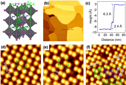
STM characterization of MAPbI3 thin films. a) Crystal structure of the orthorhombic MAPbI3 perovskite. b) Large-scale STM image of the MAPbI3 perovskite film surface (300×300 nm2, U=2.5 V, and I=30 pA). c) Height profile along the dashed line in (b). d–f) High-resolution STM images of the zigzag and dimer structures (43×43 Å2, U=2.5 V, and I=50 pA), with two structures coexisting in the same terrace (56×56 Å2, U=2.5 V, and I=50 pA). The unit cells are highlighted by dashed rectangles. Inset in (f): The height profile reveals a height difference of less than 10 pm. All panels are reproduced from Ref. 18m with permission. Copyright 2016 American Chemical Society.
3.1.3 Mixed-Halide Perovskites
Mixing the halide compositions of the MHPMs can have a significant impact on their properties and stability.33 It has been reported that the incorporation of a small amount of Cl in MHPMs can improve the stability,34 extend the lifetime of carrier recombination,35 and increase the open circuit voltage.36 However, only a few studies have explored the surfaces of mixed-halide perovskites,37 and the role of Cl in MHPMs remains elusive.38 In this case, direct characterization of the precise location of the incorporated Cl in mixed perovskites is the best way to clarify these issues. Qi and co-workers conducted STM investigations by incorporating a small amount of different types of halogen ions (I or Cl) into MAPbBr3 to unravel the role of the halogens in the mixed-halide perovskite.18i High-resolution STM images revealed MA–halogen surface terminations for the (001) surface of the pristine MAPbBr3 as well as the MAPbBr3−yI, and MAPbBr3−zClz mixed-halide perovskites (Figure 4 a–c). The STM topography images revealed bright and dark protrusions accompanied by different apparent heights and widths, which were different from the pristine MAPbBr3 surface, where all the Br anions had the same height and width (Figure 4 d). The apparent height of the bright protrusions was (40±10) pm greater than the surrounding Br ions, which are also larger in diameter, according to the line profile (Figure 4 e). In contrast, the dark protrusions were (20±10) pm lower than the neighboring Br ions (see Figure 4 f). The bright protrusions were assigned to I anions because their ionic radii are larger than those of Br anions, and the dark protrusions were assigned to the Cl anions because of their smaller ionic radii. It is noteworthy that these bright or dark protrusions were randomly distributed on the surface. Complementary information gained from fast Fourier transform (FFT) of the STM images clearly revealed a quasi-square unit cell that was consistent with the (001) plane of the orthorhombic structure. The FFTs of the STM images of MAPbBr3−yIy and MAPbBr3−zClz were similar to that of pristine MAPbBr3, which indicates no surface structure change and is in agreement with theoretical calculations.37b, 39 The calculations indicated that the substitution of Br by I (or Cl) is energetically favorable, and the corresponding simulated STM images exactly duplicated the results observed in the experiment (Figure 4 g–i), especially with the height differences of I and Cl ions relative to Br ions being calculated to be +0.35 Å and −0.24 Å, respectively. These values are in good agreement with the STM measurements.
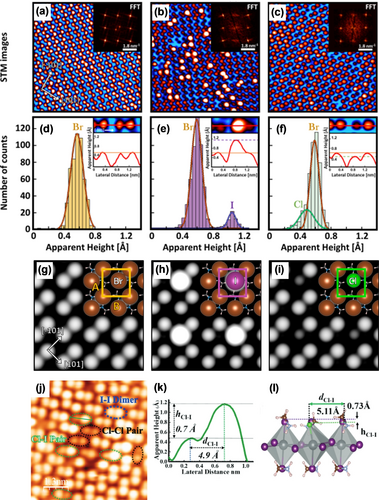
Detailed structural characterization of mixed-halide perovskites. High-resolution STM images of a) the pristine MAPbBr3 surface (10×10 nm2, U=1.3 V, and I=80 pA), b) the MAPbBr3−yIy surface (10×10 nm2, U=2.0 V, and I=120 pA), and c) the MAPbBr3−zClz surface (10×10 nm2, U=−2.0 V, and I=100 pA). The bright and dark protrusions are assigned to iodine and chlorine ions, respectively, which substitute Br ions at the surface. Inset: FFT images obtained from the corresponding topographic STM images. d–f) Histograms of the apparent height distribution of the local maxima (i.e. the ions). The major peaks correspond to the Br ions, while the minor peaks are associated with iodine and chlorine ions. Inset: typical profiles obtained for the different halides (Br, I, Cl) at the perovskite surface. g–i) Calculated (001) surface of g) pristine MAPbBr3, h) MAPbBr3−yIy, and i) MAPbBr3−zClz. Inset: the corresponding surface model and unit cell. Panels (a–i) are reprinted from Ref. 18i with permission. Copyright 2019 American Chemical Society. j) High-resolution STM images of the MAPbI3−xClx surface (14.5×14.5 nm2, U=−2.5 V, and I=50 pA). k) Line profile of the Cl-I pair along the green line in (j). l) DFT model for the Cl-I pair showing the height and length. Panels (j–l) are reprinted from Ref. 18j with permission. Copyright 2021 The Royal Society of Chemistry.
Qi and co-workers revealed the atomic-scale surface structure of the mixed-halide perovskite MAPbI3−xClx.18j In addition to I-I dimers, Cl-I pairs with different heights and widths can also be distinguished (Figure 4 j). The average height of the incorporated Cl ions is about 0.7 Å lower than the neighboring I ions (Figure 4 k,l). Unlike the case of the incorporation of Cl ions into the MAPbBr3 perovskite, Cl-Cl dimers were also observed in MAPbI3−xClx, thus indicating that the Cl-Cl dimer had a total energy similar to that of the Cl-I dimer, which was also confirmed by DFT calculations. Here three important points need to be emphasized: 1) the substitution reaction of an I ion by a Cl ion occurs not only in the dimer structure but also in the zigzag structure; 2) a certain amount of Cl ions can be mixed into MAPbI3, but most of the Cl ions incorporated on the surface prefer to be near the grain boundaries rather than at the center of the grains, and this inhomogeneous surface phenomenon has been reported previously;40 3) Cl ions are incorporated in both the surface and sub-surface layers of MAPbI3, which have a pronounced impact on the electronic properties and stability of the MAPbI3−xClx perovskite. These findings not only reveal the precise location of the Cl and I anions in the mixed halide perovskites but also provide an answer to the extent of their incorporation in the crystal lattice.
3.1.4 CsPbBr3
All-inorganic metal halide perovskites show better stability than the organic-inorganic metal halide perovskites;41 for example, they can withstand the flux of electrons required for electron microscopy. Although high-angle annular dark field (HAADF) imaging by scanning transmission electron microscopy (STEM) revealed the surface structure of CsPbBr3 single crystals with atomic resolution, the relatively weak signal of the Br-terminated CsPbBr3 surface led to difficulty in observing the surface Br ions in detail.42 Qi and co-workers for the first time reported the growth of ultrathin CsPbBr3 films with a thickness of approximately (4±1) nm on a clean Au(111) surface by dual-source evaporation.18o Similar to the organic-inorganic hybrid metal halide perovskites, two distinct surface rearrangement patterns co-existed on the same terrace. These two domains were observed in four different orientations rotated by ±45° and ±90° with respect to one another (Figure 5 a). To further understand these two different structures, DFT calculations were carried out. The bright spots were assigned to the Br anions of the CsBr-terminated (001) surface of the orthorhombic crystal structure with the Pnma space group. As a consequence of the lower density of states (DOS), the Cs cations could not be resolved in the STM images. Based on the STM observations and DFT calculations, the stripe pattern of the bright spots can be represented as a rectangular unit cell with lattice constants of A=7.3 Å and B=14 Å (Figure 5 b). In contrast, the armchair patterns consist of alternating rows of bright and dark Br pairs with lattice parameters of c=11.8 Å and d=11.6 Å (Figure 5 c) for the quasi-square unit cell. This alternating bright and dark surface reconstruction is caused by a change in the vertical position of the surface Br and Cs ions along the [101] direction (Figure 5 c). Interestingly, the spherically symmetric Cs+ ion would not lead to rearrangement of the surrounding Br− ions because of its nonpolarity. However, two distinct rearrangement patterns of the surface atoms can be distinguished clearly by STM. Moreover, the stripe structure is energetically more favorable than the armchair structure. This means that the stripe structure has higher surface stability than the armchair structure, which is consistent with the experimental observations that the stripe domains were found to be more abundant on the surface. Liang and co-workers revealed through DFT calculations that the nonpolar CsBr-terminated (001) surface showed the highest stability compared to the polar surface.43 This is consistent with the experimental observations by STEM and STM.
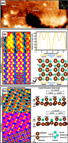
Surface structure of the CsPbBr3 perovskite. a) Large-scale STM image of the CsPbBr3 perovskite with the typical orientations of the stripe and armchair domains (29×12 nm2, U=2.17 V, and I=30 pA). Experimental high-resolution STM image (top), simulated STM image (middle), and crystal structure model (bottom) of b) the stripe structure (3.9×2.8 nm2, U=2.3 V, and I=50 pA) and c) armchair structure (5.2×4.2 nm2, U=2.0 V, and I=100 pA). The unit cells for the two structures are marked in a rectangular and quasi-square shape, respectively. The lattice parameters are consistent with the crystal structure model. Color code: Cs green, Br brown. All panels are reproduced from Ref. 18o with permission. Copyright 2020 American Chemical Society.
In the section above, we have discussed the nature of the surface structures of MHPMs. In the next section, we focus on their electronic properties, which greatly impact the performance of PSCs.
3.2 Electronic Structures and Fermi Level Position
Scanning tunneling spectroscopy (STS) is the method of choice to determine the local density of states (LDOS) at the surface. Ultraviolet photoemission spectroscopy (UPS) and inverse photoemission spectroscopy (IPES) can measure the energy positions of the valence band maximum (VBM) and conduction band minimum (CBM) at the surface of semiconductors. Figure 6 a presents a typical STS dI/dV spectrum for cleaved MAPbBr3 recorded at 4.5 K, which shows that the major contribution to the LDOS originates from the occupied state, while the unoccupied state does not show an appreciable differential conductance.18e This is in good agreement with the partial density of states calculations, which suggests that the DOS is derived from the orbitals of Br (major contribution) and the orbitals of the C and N atoms of MA (minor contribution; Figure 6 b). Special attention should be paid to the surface reconstructions and the variation of their electronic properties. The LDOS of zigzag (ferroelectric) and dimer (antiferroelectric) domains exhibited a small difference in the energy positions of the orbitals (for details see the inset of Figure 6 b). This small difference might have an impact on the local light-harvesting properties and interfacial coupling of perovskites.18e Figure 6 c presents the dI/dV spectra of the cleaved MAPbBr3 acquired at RT, which reveals the different onset of the valence and conduction bands. A strong increase in the signal intensity was observed under irradiation with light, which indicates the generation of additional free charge carriers and tunneling channels.18e Kahn and co-workers determined the band gap of MAPbBr3 films on top of a TiO2/FTO substrate to be 2.30 eV through a combination of UPS, IPES, and DFT calculations.44 The intensity peaks near the valence band were dominated by the contribution of the Br 4p orbital, with minor contributions from the Pb 6s and 6p orbitals. In the case of the unoccupied side, the bottom of the conduction band was dominated by the contribution of the Pb 6p orbital, with a minor contribution from the Br 4p orbital (Figure 6 d).44 This is similar to the results reported by Qi and co-workers,18e except that the Fermi level position in the band gap was found to be closer to the conduction band (CB) side, which may be caused by the different methods of sample preparation and the type of substrates.45 In a separate measurement of MAPbBr3 single crystals by angle-resolved photoemission spectroscopy (ARPES), Fauster and co-workers demonstrated that the phase transition from the orthorhombic to the cubic structure would directly affect the surface electronic structure.46 Interestingly, Rashba splitting was detected not only in the orthorhombic phase of MAPbBr3, but also in the cubic phase,46, 47 which may arise from surface polar reconstruction phenomena or induced by strain.13b, 48 The electronic structure of MAPbI3 and the position of the Fermi level has been reported by several research groups.18m, 44, 45, 49 The typical dI/dV spectra for deposited MAPbI3 presented in Figure 6 e,f were acquired at different sites of two types of surface structures.18m The position of the CBM is at 0.7 eV above the Fermi level (V=0), while the position of the VBM is at 1.0 eV below the Fermi level. This is different from the onset of the lowest binding energy for the valence band (VB) obtained by ARPES in the range of 1.3–1.4 eV,49a probably because of substrate effects. The electronic gap of MAPbI3 is about 1.7 eV, which is in good agreement with the UPS/IPES measurements44, 49b and photoluminescence (PL) measurements.50 The DOS is mainly composed of the I and Pb orbitals (Figure 6 g). Balberg and co-workers and Redinger and co-workers showed through STS measurements that the position of the Fermi level in the band gap of MAPbI3 could be changed by the different surface compositions obtained by using different synthesis routes.45c, 49c The surface inhomogeneities were revealed by the mapping image of the normalized dI/dV spectra, where two different types of local electronic signals were determined at the same crystal grains (Figure 6 h).37c, 49d The positions of the Fermi energy level of MAPbI3 films were also influenced by the substrates.45a, 45b
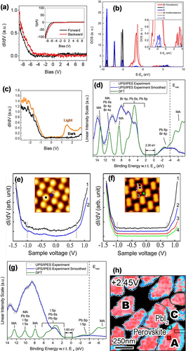
Electronic properties of perovskite materials. a) dI/dV spectra of orthorhombic MAPbBr3, obtained in the forward and backward directions. Inset: Corresponding I(V) spectrum. b) Comparison of density of states calculations on two different domains: polar (solid line) and nonpolar (dotted line). Inset: Enlargement of the energy region close to the Fermi level. c) dI/dV spectra of cubic MAPbBr3. The black line was obtained in the dark and the orange line obtained under irradiation with light. Panels (a–c) are reprinted from Ref. 18e with permission. Copyright 2015 American Chemical Society. d) UPS and IPES spectra of MAPbBr3 with DFT simulations. Reprinted from Ref. 44 with permission. Copyright 2016 American Chemical Society. The typical dI/dV spectra of MAPbI3 perovskite for the e) zigzag structure and f) dimer structure, which were acquired from different sites as marked in the inset of the STM images. Panels (e,f) are reproduced from Ref. 18m with permission. Copyright 2016 American Chemical Society. g) UPS and IPES spectra of MAPbI3 with DFT simulations. Reprinted from Ref. 44 with permission. Copyright 2016 American Chemical Society. h) dI/dV mapping of MAPbI3 perovskite (U=2.45 V) with point-to-point electronic dI/dV curves. Reprinted from Ref. 49d with permission. Copyright 2017 American Chemical Society.
A small amount of Cl incorporation would not change the band gap in the bulk of the parent perovskites, which has been confirmed by UPS/IPES measurements and theoretical calculations.18i, 37b, 49b However, the work function of the mixed halide perovskite decreases after Cl substitution, but remains unchanged with iodide incorporation (Figure 7 a).18i On the basis of the DFT calculations, the projected density of states (PDOS) of MAPbBr3−yIy was composed of the orbitals of Br and MA, as well as the I 5p states, while MAPbBr3−zClz was composed from the orbitals of Br and MA, as well as Cl 3p states (Figure 7 b).18i In contrast, the incorporation of a certain amount of Cl or I ions would effectively modulate the electronic characteristics of mixed-halide perovskites.51 The UPS/IPES results showed an increased band gap of the MAPbI3−xClx perovskite after incorporation of a certain amount of Cl ions (Figure 7 c).18j Moreover, MAPbI3−xClx was also found by UPS measurements to have a larger work function than pristine MAPbI3, which is consistent with the earlier UPS measurements performed by Kahn and co-workers.49b
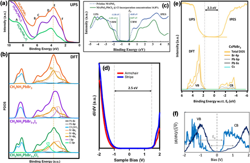
Determination of the electronic properties. a) Experimental UPS spectra of pure MAPbBr3 (orange) as well as mixed MAPbBr3−yIy (purple) and MAPbI3−xClx (green) perovskites. b) Calculated PDOS of pure MAPbBr3 (orange) as well as mixed MAPbBr3−yIy (purple) and MAPbI3−xClx (green) perovskites. The different colored lines indicate different contributions of orbitals. Panels (a,b) are reproduced from Ref. 18i with permission. Copyright 2019 American Chemical Society. c) UPS/IPES spectra of pristine MAPbI3 (dashed blue line) and mixed MAPbI3−xClx (solid green line). Reproduced from Ref. 18j with permission. Copyright 2021 The Royal Society of Chemistry. d) dI/dV spectra of CsPbBr3 perovskite for the stripe and armchair domains. e) Electronic structure of CsPbBr3 perovskite. Top: UPS-IPES spectra. Bottom: Calculated PDOS. The gray dashed lines indicate the positions of the valence band and conduction band edges. Panels (d,e) are reproduced from Ref. 18o with permission. Copyright 2020 American Chemical Society. f) dI/dV spectra of MA0.83FA0.17PbI3 perovskite. Reproduced from Ref. 54 with permission. Copyright 2020 American Institute of Physics.
The local electronic structure of the CsPbBr3 perovskite was characterized by Qi and co-workers using STS recorded at the Br ion of the stripe and armchair structure on the CsBr-terminated (001) surface.18o Surprisingly, the representative normalized dI/dV spectra for these two distinct type domains were similar (Figure 7 d). A well-defined band gap of 2.5 eV was derived from the dI/dV spectra based on the VB and CB edges. This gap is 0.2 eV larger than the value determined by UPS-IPES measurements (Figure 7 e).18o, 44, 52 Based on the exact atomic structure of CsPbBr3, DFT calculations were performed and revealed that the main contribution of the VBM originated from the Br 4p and Pb 6s orbitals, while the CBM was dominated by the Pb 6p and Br 4p orbitals (Figure 7 e), in agreement with the results of Kahn and co-workers.44
Recently, the LDOS of the mixed-cation lead halide perovskite MA0.83FA0.17PbI3 was studied by Nienhaus and co-workers. The normalized dI/dV spectra recorded in the positive forward direction and negative reverse direction were consistent with a band gap of 1.55 eV and 1.44 eV, respectively (Figure 7 f), which is closer to the optical gap of 1.6 eV measured by PL experiments.53 Interestingly, the sweep direction affects the type of perovskites, with an n-type character for MA0.83FA0.17PbI3 identified for the forward direction while a p-type character was identified for the reverse direction. Therefore, we can conclude that the type of perovskite is determined by the preparation methods, substrate effect, and voltage sweep directions, which are summarized in Table 2. A better understanding of the electronic properties of MHPMs is of paramount importance to improve the performance of perovskite solar cells.
Material |
Method |
Substrate |
Type |
Band gap [eV] |
WF |
Ref. |
||||
|---|---|---|---|---|---|---|---|---|---|---|
|
|
|
|
STS |
UPS/IPES |
XPS EF−EVBM |
DFT |
Optical |
[eV] |
|
MAPbBr3 |
cleavage |
single crystal |
p |
ca. 2.1 |
– |
– |
ca. 2.3 |
– |
– |
|
deposition |
Au(111) |
n |
– |
EF−EVBM=1.70 |
– |
– |
ca. 2.3 |
4.77 |
||
solution |
TiO2/ITO |
n |
– |
2.3 |
– |
2.3 |
– |
4.0 |
||
solution |
TiO2/FTO |
n |
– |
2.3 |
– |
– |
– |
4.0 |
||
solution |
PEDOT: PSS/ITO |
n |
– |
2.3 |
– |
ca. 2.3 |
– |
5.27 |
||
MAPbI3 |
deposition |
Au(111) |
n |
1.7 |
– |
– |
– |
– |
– |
|
solution |
TiO2/ITO |
n |
– |
1.6 |
– |
1.6 |
– |
4.0 |
||
solution |
glass |
n |
– |
EF−EVBM=1.43 |
– |
– |
1.62 |
4.21 |
||
solution |
Cu2O |
p |
– |
– |
0.9 |
1.85 |
– |
4.9 |
||
NiO |
n |
– |
– |
1.03 |
– |
4.49 |
||||
PEDOT:PSS |
n |
– |
– |
1.38 |
– |
4.43 |
||||
FTO |
n |
– |
– |
1.69 |
– |
4.22 |
||||
Al2O3 |
n |
– |
– |
1.7 |
– |
3.72 |
||||
ZnO |
n |
– |
– |
1.72 |
– |
4.64 |
||||
TiO2 |
n |
– |
– |
1.72 |
– |
4.03 |
||||
ZrO2 |
n |
– |
– |
1.77 |
– |
3.86 |
||||
solution |
sNiO/ITO |
p |
– |
1.7 |
– |
– |
– |
4.7 |
||
TiO2/ITO |
n |
– |
1.7 |
– |
– |
– |
4.0 |
|||
solution |
TiO2/FTO |
n |
– |
1.7 |
– |
– |
– |
3.99 |
||
solution |
ITO |
n |
1.58 |
|
– |
– |
– |
– |
||
solution |
TiO2/FTO |
p |
1.53 |
– |
– |
– |
1.60 |
– |
||
solution |
TiO2/FTO |
n |
1.50 |
– |
– |
– |
– |
– |
||
solution |
PEDOT:PSS/ITO |
n |
– |
1.7 |
– |
– |
– |
4.7 |
||
deposition |
Au(111) |
n |
– |
1.13 |
– |
ca. 1.2 |
– |
5.07 |
||
solution |
microcrystal |
n |
– |
EF−EVBM=1.15 |
– |
|
1.50 |
4.29 |
||
solution |
mp-TiO2/FTO |
n |
– |
EF−EVBM=1.33 |
– |
– |
1.57 |
4.02 |
||
solution |
ITO |
n |
– |
EF−EVBM=1.42 |
– |
– |
1.54 |
4.1 |
||
solution |
PEDOT: PSS/ITO |
n |
– |
1.59 |
– |
ca. 1.6 |
– |
4.42 |
||
MAPbBr3−yIy |
deposition |
Au(111) |
n |
– |
EF−EVBM 1.80 |
– |
<2.3 |
– |
4.79 |
|
MAPbBr3−zClz |
deposition |
Au(111) |
n |
– |
EF−EVBM=1.65 |
– |
ca. 2.3 |
– |
4.57 |
|
MAPbI3−xClx |
solution |
TiO2/FTO |
n |
– |
1.7 |
– |
– |
– |
4.14 |
|
deposition |
Au(111) |
n |
– |
1.62 |
– |
ca. 1.4 |
– |
4.76 |
||
MAPbBr3(Cl) |
solution |
TiO2/FTO |
– |
– |
– |
– |
– |
– |
4.5 |
|
solution |
PEDOT:PSS/FTO |
– |
– |
– |
– |
– |
– |
5.1 |
||
CsPbBr3 |
deposition |
Au(111) |
p |
2.5 |
2.3 |
– |
2.3 |
– |
4.72 |
|
solution |
TiO2/ITO |
n |
– |
2.3 |
– |
2.3 |
– |
4.1 |
||
solution |
ZnO/ITO |
p |
– |
EF−EVBM≈1.1 |
– |
– |
2.37 |
4.7 |
||
deposition |
ITO |
n |
– |
EF−EVBM=1.75 |
– |
– |
2.33 |
3.98 |
||
solution |
ITO |
– |
– |
EF−EVBM=1.18 |
– |
– |
– |
4.46 |
||
MA0.83FA0.17PbI3 |
solution |
ITO |
n |
1.55 (F)[b] |
– |
– |
– |
1.6 |
– |
|
MA0.83FA0.17PbI3 |
solution |
ITO |
p |
1.44 (R)[b] |
– |
– |
– |
1.6 |
– |
|
FA0.83Cs0.17PbI3 |
solution |
SnO2/FTO |
n |
– |
1.81 |
– |
1.57 |
– |
3.91 |
|
- [a] EF: Fermi level; EVBM: valance-band maximum; WF: work function; ITO: indium-doped tin oxide; FTO: fluorine-doped tin oxide; PEDOT: PSS: poly(3,4-ethylenedioxythiophene):polystyrene sulfonate; sNiO: sol-gel nickel oxide; mp-TiO2: mesoporous-TiO2. [b] F and R denote the forward direction and reverse direction of the dI/dV spectra.
3.3 Surface Structure Transition under External Stimuli
Using STM, surface reconstruction behavior was observed for MAPbBr3, MAPbI3, and CsPbBr3. The surface reorientation of Br dimers was revealed in sequential STM images for the deposited MAPbBr3, where the Br dimer rotated by 90° relative to its original orientation (Figure 8 a). This could be interpreted as the dissociation and reassociation of the Br− pair.18f The reason for this reorientation was essentially the realignment of the dipole of the MA+ group, which arises from an in-plane rotation of MA+ in response to an electric field. The rotation of MA+ led to dissociation of the Br dimer and further rotation resulted in the formation of the new dimer structure with other neighboring Br ions (Figure 8 b). Notably, MAPbBr3 was kept at a low temperature range of 4.6–180 K for STM observations. Even at such low temperatures, the surface reorientation was still observed, which indicates a low transition energy barrier. The calculations revealed that when Br− and MA+ moved together, the system energy did not change from a lower transition energy of 0.46 eV (Figure 8 c).18f This suggests that the surface reorientation of Br dimer is reversible. Similar to the case of MAPbBr3, two types of surface structures for MAPbI3—the dimer and zigzag domains—can be reversibly transformed by applying a voltage pulse (Figure 8 d–f).18m The phase transition energy barrier between two the distinct structural domains was calculated to be 0.18 eV per unit cell. The calculated value of the rotational barrier for the MA+ cation was around 50 meV. This relatively low energy barrier means that rotation can occur during the STM operation, which is consistent with the previously reported studies.55
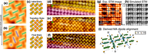
Surface reconstruction under external stimuli. a,b) Consecutive STM images of the MAPbBr3 perovskite, showing the shift in the dimer structure orientation (2.3×2.3 nm2, U=−9.0 V, and I=20 pA). c) Simulated reorientation of the dimer structure, including initial, transition, and final states. Color code: N blue, C gray, H white, Br brown. Panels (a-c) are reproduced from Ref. 18f with permission. Copyright 2019 American Chemical Society. d–f) Consecutive STM images of MAPbI3 showing the reversible transition between the dimer and zigzag structures: d) U=2.0 V, e) U=0.85 V, and f) U=−1.25 V (4.2×12.8 nm2, I=30 pA). Panels (d–f) are reproduced from Ref. 18m with permission. Copyright 2016 American Chemical Society. g,h) Experimental and simulated STM images of the (4×2) structure of MAPbBr3 under laser illumination. i) Model of the MA orientation pattern. Panels (g–i) are reproduced from Ref. 18d with permission. Copyright 2019 American Chemical Society.
In addition to external electrical stimuli, a photodriven molecule dipole reordering of the cleaved MAPbBr3 crystal surface was reported by Chiu and co-workers.18d The (2×2) dimer structure on the MAI-terminated (001) face was observed under dark conditions (Figure 3 e). This (2×2) dimer structure could be transformed into a new (4×2) surface structure under laser illumination (Figure 8 g,h). This new (4×2) structure was related to rearrangement of the dipole orientation of the MA cation. This phase transition was reversible, namely, when the illumination was removed, the (2×2) dimer phase was reformed, thus indicating that the laser illumination did not decompose the MA cations. With the support of DFT calculations, the underlying mechanism was proposed to be a photo-driven separation of electron–hole pairs in spatially displaced orbitals, which generates polarization fields that lead to the rearrangement of polarized MA cations (Figure 8 i). The tilting of the MA+ dipoles in the centers of the bright (B-B′) and dark (C-C′) stripes led to a change in the degree of dipole polarization, which in turn caused a difference in the repulsive or attractive force exerted on the Br ions. This difference resulted in the dipole negative siding up in the bright stripes (B-B′) and the positive siding up in the dark stripes (C-C′). In addition, the dipoles between the MA+ cations must be oriented in-plane and alternatingly point toward the B-B′ and C-C′ lines.
Although the two types of surface domains were observed on the CsBr-terminated (001) surface, the surface reorientation has not been observed for CsPbBr3;18o this indicates a more stable surface structure probably because of the stronger Coulomb interactions.56
3.4 Surface Defect Dynamics
Recent findings suggested that the role of defects is crucial for the further development of PSCs, because they would have a direct impact on the structural stability, carrier recombination, and charge-transfer properties.7b, 17, 57 The nature and formation mechanism of point defects in MHPMs have been studied using DFT calculations.23c, 23f, 58 However, investigation of these point defects experimentally remains difficult, and so far only a very few studies have been reported on this topic.18e, 18f, 18m, 57i Recently, the atomic-scale surface structure of deposited MAPbBr3 was characterized in detail by Qi and co-workers through STM combined with DFT calculations (Figure 9 a).18f Two distinct types of intrinsic point defects—unpaired Br anions and vacancies—were observed on the MABr-terminated (001) surface. The unpaired Br anion was frequently found in cases where there was a pair of mismatched orientations in the same row and they were isolated from each other (Figure 9 b). In contrast, if there was a vacancy adjacent to the Br anions, two adjacent unpaired Br defects could be formed (Figure 9 c). Various types of depression vacancies were observed, including single, double, and triple defects (Figure 9 d–f, respectively). DFT calculations showed that the formation of MABr vacancies was more energetically favorable compared to the Br anion vacancies. Similar results were also reported by Li and co-workers,23f where the simulated model (Figure 9 g) and STM image (Figure 9 h) are in good agreement with the experimental STM observations. For a single MABr vacancy, there is a nearby MA cation rotated 90°, with the positive nitrogen end of the dipole near the unpaired Br anion (Figure 9 i). In this case, the formation energy was calculated to be 1.94 eV for single MABr vacancies, 3.49 eV for double vacancies, and 5.26 eV for triple MABr vacancies.18f The presence of vacancies assisted the migration of ions and a lower transition energy barrier was expected when MABr ions migrated together in proximity to a vacancy.
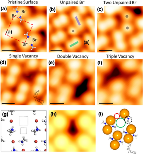
STM characterizations of surface defects. High-resolution STM image of a) pristine MAPbBr3 perovskite with MA+ overlaid to show the relative position (16×16 Å2, U=−9.0 V, and I=20 pA), b) an unpaired Br anion defect (20×20 Å2, U=−9.0 V, and I=20 pA), c) two adjacent unpaired Br anion defects with a vacancy (18×18 Å2, U=−9.0 V, and I=20 pA), d) a single vacancy defect (18×18 Å2, U=−3.0 V, and I=100 pA), e) double vacancy defects (17×17 Å2, U=−9.0 V, and I=20 pA), and f) triple vacancy defects (16×16 Å2, U=−9.0 V, and I=20 pA). Panels (a–f) are reproduced from Ref. 18f with permission. Copyright 2019 American Chemical Society. g) Calculated model of a MABr vacancy. The squares show the position of the missing Br and MA ions. Color code: N blue, C gray, H white, Br brown. h) Simulated STM image of a MABr vacancy. The STM image was calculated for a W(111) tip. Panels (g,h) are reproduced from Ref. 23f with permission. Copyright 2017 American Chemical Society. i) The model slab for a single vacancy defect. Color code: N blue, C gray, H white, Br brown. Reproduced from Ref. 18f with permission. Copyright 2019 American Chemical Society.
Similar surface defects were also observed by Qi and co-workers18e and Zhong and co-workers18m for cleaved MAPbBr3 and deposited MAPbI3 perovskite films, respectively. In general, mechanical cleavage does not create intrinsic defects,22 while the deposited perovskite thin films often contain atomic-scale surface defects.18f, 18m, 18n Significantly, the surface vacancies could act as adsorption sites for oxygen or H2O molecules, thereby resulting in decomposition.23f, 59
3.5 Halide Substitution and Its Impact on Surface Stability
The poor stability of MHPMs is one of the key influencing factors that hinder their commercialization.60 As mentioned above, the incorporation of a small amount of chlorine in MHPMs can enhance their performance, as shown mainly through studies on solar cell devices.33d-34, 35, 36, 37 However, a comprehensive understanding about the exact role of incorporated Cl remains elusive.33f, 38, 61 STM studies offer deeper insights into the role of halogen in the mixed halide perovskites. Qi and co-workers conducted STM characterizations to determine the exact locations of deposited I− and Cl− ions on the surface of MAPbBr3−yIy and MAPbBr3−zClz perovskites.18i The evaporation of PbI2 may produce Pb, I, and PbI2 molecules.18n DFT calculations simulated a variety of scenarios and revealed that the most energetically favorable was the substitution of Br anions by I or Cl anions at the surface of perovskites. Cl anions preferred to form isolated Cl-Br pairs rather than the single Cl-Cl pairs. A similar trend was also found in the substitution behavior of I anions, which was consistent with the STM observations of randomly distributed anion substitution. Based on the STM observations and DFT calculations, the substitution process can be described as an initial adsorption of evaporated PbI2 (or PbCl2) molecules on the perovskite surface, and then dissociation of these molecules. The substitution reaction then occurred between the halogen atoms, and the substituted atoms diffused or desorbed on/from the surface (Figure 10 a). The Br ions adjacent to the defects are more likely to be substituted as they are less coordinated, and the chemical bond at the defect is weaker than that in the crystal.62 When the substitution ratio is less than 25 %, the incorporation of Cl anions results in an increase in the decomposition energy, which indicates that the stability of MAPbBr3−zClz is enhanced (Figure 10 b). In contrast, when the substitution ratio exceeds this threshold, the decomposition energy decreases as the Cl content increases. The increase in the stability of MAPbBr3−zClz may be caused by the relatively stronger bond strength of Cl−Pb compared to that of Br−Pb.18i However, as the substitution ratio exceeds 25 %, the strain induced by the incorporation of the Cl ions would be increased and counteract the benefit of the Cl−Pb bond, thereby leading to poor stability. Time-evolution X-ray photoelectron spectroscopy (XPS) results indicated that the stability of the MAPbBr3 was significantly enhanced as the surface Br ions were partially substituted by Cl ions. As shown in Figure 10 c,d, MAPbBr3−zClz with 18 % Cl at the surface showed significantly higher stability than pristine MAPbBr3, where the Pb0 signal associated with the deterioration of the perovskite films emerged after 4 h of MAPbBr3 storage under an ultrahigh vacuum, while the Pb0 peak emerged after 116 h for MAPbBr3−zClz.18i
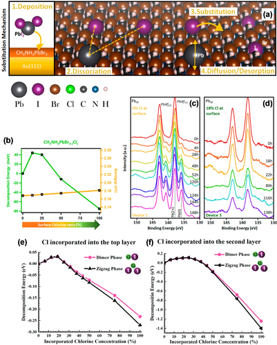
a) Schematic representation of the substitution mechanism using PbI2 as an example. b) Stability versus band gap change in the MAPbBr3−zClz perovskite. The Pb 4f core-level spectra of c) pure MAPbBr3 and d) MAPbBr3−zClz with 18 % Cl at the surface. Panels (a–d) are reproduced from Ref. 18i with permission. Copyright 2019 American Chemical Society. The calculated decomposition energy of e) the first layer and f) the second layer of MAPbI3−xClx. Panels (e,f) are reproduced from Ref. 18j with permission. Copyright 2021 The Royal Society of Chemistry.
Similarly, incorporation of a certain amount of Cl ions into MAPbI3 can enhance its stability. The optimal concentration of incorporated Cl ions was predicted to be about 18 % for the topmost layer and about 25 % for the second layer (Figure 10 e,f). Interestingly, the concentration incorporated into the subsurface layer is higher than that of the first layer, and the addition of Cl ions into the second layer seems to play a more important role in the stability of MAPbI3−xClx perovskites, which suggests that the adsorbed Cl ions not only diffuse on the surface but also migrate to the interior of the bulk by means of I vacancies. The decomposition energy of the MAPbI3−xClx perovskite exhibited a non-monotonic trend consisting of an initial increase followed by a decrease as a function of the concentration of incorporated Cl. These findings would have a great impact on the issue of perovskite stability, which is still one of the major challenges for the practical application of PSCs.
3.6 Atomic-Scale Investigation of Interfacial Structures
Modification and engineering of interfaces is useful for MHPM applications, especially since the surface topography and electronic properties of perovskite materials are highly correlated with their associated chemical and physical parameters, which can further affect the performance of the devices.5d, 16, 57i, 63 However, the fundamental understanding of the interface science of MHPMs is still at an early stage. The relationship between interfacial properties, film structure, and potential interactions has not yet been clarified. Obtaining a reliable and comprehensive picture of the interfaces would greatly help to guide film processing for achieving more efficient and stable PSCs. STM can directly provide an in-depth understanding of interface properties of MHPMs through the real-space view of atomic interface and electronic structure of heterostructures. Insight into the fundamental properties of interfaces is essential to guide the improvement and optimization of MHPMs for optoelectronics. Recently, Qi and co-workers investigated the interface properties of MAPbX3 (X=I or Br) and copper phthalocyanine (CuPc) at the atomic scale using a combination of STM and DFT calculations;18k in this case, CuPc was used as the hole transport layer (HTL) material.64 As shown in Figure 11 a, the majority of the surface was covered by MAPbI3, which exhibited characteristic surface reconstruction, while only a small area did not show this surface corrugation. A high-resolution STM image (Figure 11 b) shows a hexagonal moiré pattern with a lattice constant of 0.43 nm. This non-perovskite domain may be composed of excess precursors—either PbI2 or iodine adlayers.18n, 65 When the CuPc molecules were deposited onto the sample surface, these molecules formed a self-assembled layer with the α-polymorph structure on the MAPbI3 surface, as shown in Figure 11 c, where the bright striped domain can be observed in the lower middle part of the image; in contrast, the molecules adsorbed on the non-perovskite areas in a face-up orientation. The DFT calculations showed a weak interaction between CuPc and MAPbI3, which further revealed the importance of intermolecular interactions in the stabilization of the CuPc self-assembled layer. An enlarged view (Figure 11 d) showed that the CuPc molecules were arranged in a disordered flat-lying fashion on the non-MAPbI3 domains, rather than forming a preferential standing configuration, shown as bright stripes, which suggests a stronger interaction between the CuPc and the non-perovskite material than with MAPbI3. A similar result was obtained for CuPc on the MAPbBr3 surface, which indicates that changing the type of halide does not significantly affect the adsorption behavior of CuPc on the perovskite surface. The structurally different CuPc on non-perovskite and perovskite material would have a significant effect on the orbital overlap at the perovskite-HTL interface.18k In addition, the molecular orientation would strongly affect the device performance.66 The change of the highest occupied molecular orbital (HOMO) level of CuPc (Figure 11 e) can significantly impact the interfacial properties of the PSC, such as light absorption and interfacial charge transfer, as well as the energy level alignment at the interface. The characterization of the non-stoichiometric MHPM/CuPc interface at the atomic scale by STM is an opportunity to further understand the interfacial structure, interfacial properties, as well as the structure-interface-transport property relationship.
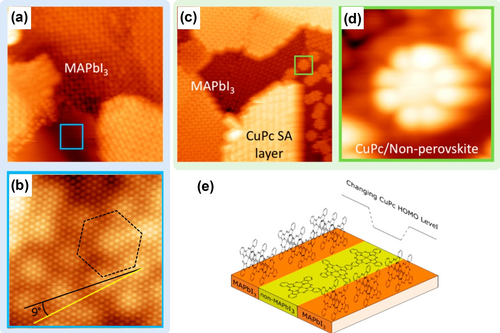
Interfacial structures and properties of CuPc on nonstoichiometric MHPMs. a) Large-scale STM image showing MAPbI3 and non-MAPbI3 (featureless area near the blue box) domains (17.6×17.6 nm2, U=−2.5 V, and I=100 pA). b) High-resolution STM image of the non-MAPbI3 domain showing a hexagonal superstructure (10.3×10.3 nm2, U=−2.7 V, and I=300 pA). c) CuPc deposited on the nonstoichiometric MAPbI3 surface showing the different adsorption behavior (26.4×26.4 nm2, U=−2.5 V, and I=100 pA). d) Enlargement of the face-on adsorbed CuPc on the non-MAPbI3 domain (3.3×3.3 nm2, U=−2.5 V, and I=100 pA). e) Schematic diagram of the CuPc HOMO energy level change. All panels are reproduced from Ref. 18k with permission. Copyright 2021 American Chemical Society.
4 Conclusion and Outlook
Even though the power conversion efficiency of PSCs has reached impressive levels, the fundamental understanding of these materials is still limited, in particular atomic-scale insights into the surface properties and their influence on device performance and stability. This Review highlights recent progress in the use of STM to study MHPMs and shine light on the basic surface properties of these materials. The surface structure and property studies using STM provide a deep understanding and enable optimization of the performance of perovskite-based devices. In this Review, we summarize the basic physical properties of perovskite crystal surfaces through in situ atomic and electronic visualizations using STM. We elucidate that the surface reconstruction of MHPMs is caused by two different MA+ in-plane orientations, as well as surface phase transition under different external stimuli. We discuss the various types of surface defects and their impact on the properties of MHPMs. Defects are one of key factors hindering the commercialization of PSCs. We determine the role of halogen ions and the exact location of them when incorporated into the perovskite crystal lattice, and also discuss that halogen ion incorporation has different effects on the electronic properties and stability of MHPMs; another focus of this Review is a discussion of the electronic properties of MHPMs. We show a summary of band gap values for MHPMs prepared by different methods and on different substrates, and discuss the determinants of Fermi level positions. Some of these insights can be generalized to assist in the rational design of new materials with desirable properties. As the field of PSCs is still rapidly growing, many new opportunities and challenges are still ahead of us.
In the following, we outline a few new research directions that warrant further investigations.
4.1 2D Halide Perovskites
As the efficiency of PSCs continues to increase, the stability of the devices has also improved significantly. In addition to the incorporation of a halogen anion in the X-site approach, a new strategy stands out amongst many other developments, namely, the generation of 2D MHPMs, which have a number of intriguing properties such as high-performance optoelectronic properties, fewer defects, suppression of anion migration, and higher stability.67 However, the fundamental properties of these 2D perovskite materials still remain to be fully understood. Vapor deposition methods are suitable for the synthesis and study of low-dimensional materials, and the STM technique with atomic resolution can provide a suitable platform for resolving and investigating these 2D structures. In particular, the study of surface structures, inherent defects, and the LDOS of 2D perovskite materials through STM/STS will provide insight into the surface properties and conversion-related optoelectronic properties.
4.2 Interface Properties
As discussed in Section 3.6, an in-depth understanding of the interface formed between the perovskite and the adjacent charge transport layer is essential for rational interface engineering and further device improvement. Although it has been recognized that the interface in PSCs devices is key to device performance and stability, dedicated interface studies are limited. STM-based techniques can provide a reliable and comprehensive picture of the interfaces between perovskites and the adjacent charge-transport layers. For example, it is possible to study the potential chemical reactions at the interface, the effects of ion migration, and measure a range of electronic characteristics of interfaces including charge transport, interfacial charge transfer, energy level alignment, and trap state population.
4.3 Understanding the Role of Defects
The presence of defects has a significant impact on the stability of the MHPMs. In the case of surface reactions, the surface defects act as reaction centers, which disrupt the structure and, therefore, have an impact on charge transport. On the other hand, defects may in turn favor the migration, dissociation, and diffusion of ions as well as the substitution of halogen ions, which may be desirable for a certain application. Comprehensive information is lacking on the nature, density, and origin of interfacial and surface defects. Hence, more studies, especially experimental, are required to better understand how defects affect MHPMs. STM can provide in situ observation of various defect types at the surface and interface of MHPMs, which will be useful for understanding the nature of defects, charge carrier dynamics, lifetime, and structural stability, and these results will help further determine the impact of defects and, thus, enable appropriate strategies to be pursued to improve the PCE of PSCs.
4.4 Degradation
An important consideration in practical applications is the degradation of perovskite absorbers. Degradation would lead to significant distortion of the structures or properties of the MHPMs. Suppressing the degradation reactions is an important way to improve the stability of MHPMs. To date, only a few in situ investigations have focused on this topic. STM allows in situ observation of degradation processes under a number of different external stimuli, such as exposure to oxygen, H2O, heat, and light. A better understanding of the degradation process in MHPMs could be used to improve the performance of PSCs.
4.5 Pb-Free Perovskites
The environmental impact of Pb in Pb-containing perovskite solar cells has led to consideration concerns. The discovery of new relevant materials to replace lead has redirected the prospects of perovskite materials. Currently, Sn-, Ge-, Sb-, and Bi-based MHPMs are considered as candidates for replacing Pb in perovskites. However, unfortunately, their applications are still limited due to their relatively low efficiency and poor stability. Therefore, it is imperative to find ways to determine the main factors that cause the relatively low efficiencies and to develop strategies to improve the performance of Pb-free perovskites. It is expected that STM could be used to reveal numerous key parameters and novel phenomena in Pb-free perovskites, which will help Pb-free perovskites achieve high efficiency and stability, eventually enabling the commercialization of Pb-free PSCs in the near future.
4.6 Atomic-Scale Dynamics
MHPM solar cells have shown extraordinary efficiencies; however, our understanding of the mechanisms of the photoelectric conversion process in perovskite solar cells is still far from complete. Dedicated mechanistic studies of the conversion process remain scarce, and the main reason for this is that it is very difficult to achieve high temporal resolution and atomic resolution simultaneously. The combination of STM with a laser provides a viable solution to in situ probing of various atomic-scale dynamics in MHPM, such as optical absorption, photoelectric conversion, charge dynamics, electron-phonon coupling, etc.13c, 13d, 18d, 18e, 50, 68 With this advanced technique, it is possible to gain insights into the internal mechanism of photovoltaics, which is of great importance for the development of PSCs, as this will provide useful guidelines for the design of high-efficiency MHPM-based photovoltaic devices.
4.7 STM Experiments under Closer to Actual Solar Cell Operating Conditions
Most of the STM studies discussed in this Review were performed under UHV and at low temperatures (e.g. liquid helium temperature or liquid nitrogen temperature). This is mainly because it is significantly more challenging to obtain stable STM operation with atomic resolution at higher temperatures and/or in an ambient air environment. On the one hand, from the point of view of obtaining a fundamental understanding, it is beneficial to study these interesting metal halide perovskite materials under low temperature and UHV conditions. On the other hand, to make stronger connections between STM results and actual materials under solar cell operating conditions, it would be helpful to study these materials under conditions closer to the real operation conditions of solar cells. In this regard, although we have seen some promising progress,18f, 53 more research efforts are needed.
4.8 Other Techniques
STM/STS studies provide fascinating opportunities to gain insight into MHPMs and has already yielded a series of exciting results. However, STM and STS have their own limitations, namely, these techniques can only probe a small surface area, and this may not be sufficient to fully characterize a larger area of a perovskite solar cell. Therefore, it is necessary to combine STM/STS studies with other characterizations to determine the microstructure of larger areas of a solar cell. MHPMs are sensitive to high-energy electron bombardment, but are more tolerant to low-energy electrons.14c, 18e, 18o Low-energy electron diffraction or other low-energy electron-based techniques can be used to characterize a larger area of a perovskite solar cell.
Acknowledgements
This work was supported by funding from the Energy Materials and Surface Sciences Unit of the Okinawa Institute of Science and Technology Graduate University, the OIST R&D Cluster Research Program, the OIST Proof of Concept (POC) Program, JSPS KAKENHI Grant Number JP18K05266, and JST A-STEP Grant Number JPMJTM20HS, Japan.
Conflict of interest
The authors declare no conflict of interest.
Biographical Information
Yabing Qi is Professor and Unit Director of Energy Materials and Surface Sciences Unit at the Okinawa Institute of Science and Technology Graduate University in Japan, and a Fellow of the Royal Society of Chemistry. He received his B.S., M.Phil., and Ph.D. from Nanjing University, Hong Kong University of Science and Technology, and UC Berkeley, respectively. His research interests include surface/interface science, perovskite solar cells, batteries, organic electronics, energy materials, and devices.


