Stimuli-responsive photoluminescent copper(I) halides for scintillation, anticounterfeiting, and light-emitting diode applications
Abstract
Highly sensitive stimuli-responsive luminescent materials are crucial for applications in optical sensing, security, and anticounterfeiting. Here, we report two zero-dimensional (0D) copper(I) halides, (TEP)2Cu2Br4, (TEP)2Cu4Br6, and 1D (TEP)3Ag6Br9, which are comprised of isolated [Cu2Br4]2−, [Cu4Br6]2−, and [Ag6Br9]3− polyanions, respectively, separated by TEP+ (tetraethylphosphonium [TEP]) cations. (TEP)2Cu2Br4 and (TEP)2Cu4Br6 demonstrate greenish-white and orange-red emissions, respectively, with near unity photoluminescence quantum yields, while (TEP)3Ag6Br9 is a poor light emitter. Optical spectroscopy measurements and density-functional theory calculations reveal that photoemissions of these compounds originate from self-trapped excitons due to the excited-state distortions in the copper(I) halide units. Crystals of Cu(I) halides are radioluminescence active at room temperature under both X- and γ-rays exposure. The light yields up to 15,800 ph/MeV under 662 keV γ-rays of 137Cs suggesting their potential for scintillation applications. Remarkably, (TEP)2Cu2Br4 and (TEP)2Cu4Br6 are interconvertible through chemical stimuli or reverse crystallization. In addition, both compounds demonstrate luminescence on-off switching upon thermal stimuli. The sensitivity of (TEP)2Cu2Br4 and (TEP)2Cu4Br6 to the chemical and thermal stimuli coupled with their ultrabright emission allows their consideration for applications such as solid-state lighting, sensing, information storage, and anticounterfeiting.
1 INTRODUCTION
Solid-state luminescent materials continue to attract the interest of industry and academic researchers due to the current and future technological needs. Especially in recent years, the search for advanced materials, often referred to as smart luminescent materials, has received significant attention owing to their switchable optical properties (e.g., emission wavelength and intensity) in response to various physical and/or chemical stimuli.[1, 2] These switchable and tunable optical properties can be obtained by achieving phase or structural change of the subject materials with the help of external stimuli such as light, pressure, temperature, magnetic field, X-ray radiation, chemical exposure, etc.[3-5] Therefore, smart luminescent materials may offer diversified potential applications in areas such as sensing, high-level security, information storage, anticounterfeiting, scintillation, etc.[6-9] In literature, organic dyes and polymers have been extensively studied as potential smart luminescent materials due to their structural versatility and tunability.[2, 5, 7, 10, 11] However, their weak photoluminescence (PL) efficiency, structural aggregation, and concentration quenching of organic entities limit their potential practical applications.[12-16] To address these shortcomings of organic molecules, luminescent metal-organic frameworks (MOFs), transition metal complexes, nanomaterials, rare-earth doped materials, various metal halides (e.g., containing Mn2+, Pb2+, and Sb3+), have been explored in the past decade.[1, 3, 4, 6, 8, 17, 18] Although some progress has been made, a few concerns relating to the materials developed so far still need to be addressed suitably, such as complex synthesis procedures and harsh reaction conditions (e.g., MOFs), aggregation (e.g., for quantum dots), rapid phase degradation (e.g., lead halide perovskites), high cost (e.g., rare-earth metal-containing materials), environmental toxicity (e.g., lead-based materials), lack of the tunability of emission wavelength (e.g., Mn(II) and Sb(III) based emitters), etc.
Among the candidate alternative luminescent materials are the copper(I) halides, which have attracted tremendous attention in the past decade due to their low cost, low environmental toxicity, earth-abundant elemental compositions, low-temperature solution processibility, tunable structural dimensionality, and very high-efficiency light emission properties. Although many copper(I) halides have been structurally known for decades,[19-23] there is a strong renewed interest in them due to recent discoveries of their outstanding photophysical properties. For example, all-inorganic copper(I) halides such as K2CuX3, Rb2CuX3, and Cs3Cu2X5 (X = Cl, Br, and I) were all recently found to be excellent blue light emitters, which ignited the ongoing research into this exciting new class of light-emitting materials.[24-27] These low-dimensional (0D–1D) copper(I) halides demonstrate large Stokes-shifted PL emissions with PL quantum yield (PLQY) values up to 100% at room temperature. Important for materials design, the structurally isolated copper-halide units in copper(I) halides facilitate increased charge localizations and a strong quantum confinement effect within these units. In turn, these promote the formation of room-temperature stable excitons upon photoexcitation, which results in the intrinsic deformation of a crystal lattice. Therefore, luminescent copper(I) halides usually demonstrate self-trapped exciton (STE) based emission with large Stokes shift values.[28-32] Noteworthy, the ultrabright light emission with high PLQY in all-inorganic copper(I) halides is insensitive to the substitution on the alkali metal and halogen sites, as copper 3d and 4s orbitals dominate the valence band maxima (VBM) and conduction band minima (CBM).[31] Moreover, some Cu(I) halides suffer from poor environmental stability due to the oxidation of copper (from Cu+ to Cu2+). The replacement of copper(I) with silver improves air stability; however, the emission efficiency of alkali silver halides is much lower than that of the copper(I) halides.[33, 34]
Another strategy for addressing the poor stability and lack of emission wavelength tunability issues of luminescent all-inorganic copper(I) halides is the replacement of alkali metal cations with organic cations to form hybrid organic-inorganic copper(I) halides. The resultant hybrid copper(I) halides demonstrate diverse structural building blocks, improved ambient air stability, and tunable photoemission properties.[28, 35-47] In hybrid Cu(I) halides, hydrophobic organic cations surrounding the inorganic anionic units can act as a protective layer, preventing copper oxidation and thereby improving their ambient air stability. Moreover, unlike all-inorganic copper(I) halides predominantly featuring tetrahedral CuX4 building blocks, the inclusion of structurally diverse organic cations prompts the formation of a variety of coordination environments around Cu(I), including but not limited to linear, trigonal planar, tetrahedral, and combinations thereof. The coordination environment preference in Cu(I) halides usually depends on the structural flexibility, size, and shape of the organic cations.[19] For example, the smaller methylammonium (MA) cation favors the formation of edge-sharing tetrahedral [Cu2Br6]4− units in (MA)4Cu2Br6, while the use of bulky tetraphenylphosphonium (TPP+) cation results in the formation of linear [CuBr2]− units to maintain the charge balance in (TPP)CuBr2.[41, 45] In addition, emission wavelength tunability from blue to orange can be achieved in these hybrid copper(I) halides mainly by modulating the anionic copper clusters, which can be done by using different organic cations. Although the relationship between the chemical content (e.g., organic cation choice), structure (e.g., the Cu(I) coordination environment) and optical properties is not well understood, investigations suggest that high emission efficiency is obtained when both VBM and CBM are dominated by the atomic orbitals of Cu(I).[28, 30] The ability of the structurally versatile organic cations to diversify the coordination geometry of Cu(I) is noteworthy, leading to the modulation of the emission wavelength of the materials, making the hybrid copper(I) halides fascinating platform for the in-depth exploration of environmentally friendly single component multi-responsive smart luminescent materials for desirable practical applications.
This study focuses on (TEP)2Cu2Br4, (TEP)2Cu4Br6, and (TEP)3Ag6Br9 featuring tetraethylphosphonium (TEP) cation. The use of TEP follows a hypothesis that adaptable and flexible organic cations (as opposed to rigid aromatic cations) may stabilize multiple structural building blocks resulting in structural diversity. Indeed, (TEP)2Cu2Br4 has been previously reported to feature an unusual dimeric [Cu2Br4]2− anions in the structure.[23] The structural work conducted in this study confirms that (TEP)2Cu2Br4 has a 0D crystal structure featuring TEP+ cations and isolated [Cu2Br4]2− anions made of edge-sharing trigonal planar units. The newly discovered (TEP)2Cu4Br6 also has a 0D structure but features a unique star-shaped [Cu4Br6]2− inorganic cluster unit. On the other hand, the new compound (TEP)3Ag6Br9 possesses a 1D crystal structure containing isolated 1D chains separated by TEP+ cations. While (TEP)3Ag6Br9 is found to exhibit quenched PL, (TEP)2Cu2Br4 and (TEP)2Cu4Br6 demonstrate ultrabright greenish-white and orange emissions, respectively, with near unity PLQYs. To understand their emission mechanism, the experimental studies of the optical properties of these compounds are supported by our computational work. In addition to efficient PL emission, (TEP)2Cu2Br4 and (TEP)2Cu4Br6 demonstrate promising radioluminescence (RL) at room temperature under both X- and γ-rays exposure, suggesting their potential for scintillation applications. (TEP)2Cu2Br4 and (TEP)2Cu4Br6 are found to melt congruently, which can enable their melt-processing, with quenched light emission in their liquid states. Interestingly, (TEP)2Cu2Br4 and (TEP)2Cu4Br6 can also be converted into one another, accompanied by the switching of their emission colors, in the presence of different solvents or by reverse crystallization. The high sensitivity of these materials to external chemical and thermal stimuli makes them candidate smart materials with potential applications in anticounterfeiting, information storage, high-level security, sensing, etc. Prospects of these materials in various applications are discussed together with a proof-of-concept demonstration of their use in solid-state lighting. Importantly, this work provides materials design strategies for the preparation of melt- and solution-processable, low-cost, and environmentally friendly copper(I) based luminescent smart materials.
2 RESULTS AND DISCUSSION
2.1 Synthesis and structure
(TEP)2Cu2Br4, (TEP)2Cu4Br6, and (TEP)3Ag6Br9 single crystals (up to 2, 1, and 0.3 cm long, respectively) can be grown via the solvent evaporation of the saturated solution of starting materials in DMF (see the experimental section). While (TEP)2Cu2Br4 and (TEP)3Ag6Br9 crystals are colorless, (TEP)2Cu4Br6 crystals are light yellowish (Figure 1G–I and Figure S1) under ambient light. The phase purity and crystallinity of the as-synthesized samples were confirmed by the room-temperature powdered X-ray diffraction (PXRD) measurements (Figure S2).
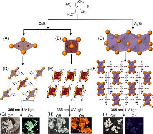
In comparison, (TEP)3Ag6Br9 adopts orthorhombic space group Pnma featuring 1D chains separated by the TEP+ cations (see Figure 1C,F). The the chain contains three crystallographically unique Ag positions, where each Ag atom is coordinated with four Br– in a slightly distorted tetrahedron. Three AgBr4 tetrahedra join by sharing edges to form an Ag3Br6 building block, further assembled into a double chain extending along the a-axis via edge-sharing connections (see Figure S6). The Ag–Br bond distances and Br–Ag–Br bond angles vary from 2.633 to 2.821 Å and from 95.39° to 124.253°, respectively. Notably, edge-sharing connectivity of AgBr4 tetrahedra in the double chains results in short Ag···Ag distances (see Figure S6 and Table S5). In this system, the Ag···Ag distances range from 3.349 to 3.595 Å, which are comparable to the sum of the van der Waals radii of two Ag atoms (3.44 Å).[53] These Ag···Ag short distances indicate the existence of argentophilic interactions and may facilitate the intramolecular electronic transitions along the polymeric chain.[54, 55]
2.2 Optical and electronic properties
The optical properties of the prepared materials have been investigated by solid-state diffuse reflectance, steady-state photoluminescence excitation (PLE), and emission (PL) measurements (see Figure 2 and Figure S7). (TEP)3Ag6Br9 is a very weak emitter (Figure 1I), and the obtained absorption, PLE and PL spectra for this compound are largely similar to that of the precursor organic salt (see Figure S7). Therefore, photoemission in (TEP)3Ag6Br9 is tentatively assigned to the organic structural component (see SI for further discussion).
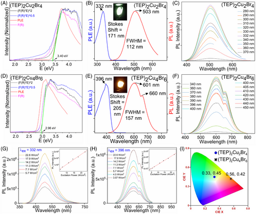
The experimental bandgaps of (TEP)2Cu2Br4 and (TEP)2Cu4Br6 from the corresponding Tauc plots (Figure 2A,D) are 3.40 and 2.96 eV (fit for a direct transition), respectively. The small bandgap of (TEP)2Cu4Br6 is also corroborated by the light yellowish color of its single crystals under daylight. The bandgaps of the Cu(I) halides are significantly smaller than the 4.28 eV bandgap of TEPBr (see Figure S7). This suggests that orbitals of inorganic units in these two-hybrid copper(I) halides have a higher band edge contribution compared to the organic molecules. Noticeably, the experimental absorption edges of both compounds are closer to their excitation peak maxima (Figure 2A,D). The single crystals of (TEP)2Cu2Br4 and (TEP)2Cu4Br6 emit ultrabright greenish-white and orange light under 365 nm UV light irradiation (see Figure 1G–H). The corresponding Commission Internationale de l'Eclairage (CIE) color coordinates of (TEP)2Cu2Br4 and (TEP)2Cu4Br6 are (0.33, 0.45) and (0.56, 0.42), respectively, as determined from the emission spectra of the compounds (Figure 2I). (TEP)2Cu2Br4 single crystals produce a broad emission peak with maximum (PLmax) at 503 nm (2.47 eV), full width at half-maximum (FWHM) of 112 nm, and a large Stokes shift of 171 nm for the excitation (PLEmax) at 332 nm (3.73 eV) (Figure 2B). The emission spectrum of (TEP)2Cu4Br6 single crystals is characterized by a broad peak with PLmax at 601 nm (2.06 eV), FWHM of 157 nm, and a large Stokes shift of 205 nm for the excitation at 396 nm (3.13 eV) (Figure 2E). The large Stokes shifts result in negligible self-absorbance, contributing to the high emission efficiency of the hybrid materials. These types of broadband emissions with large Stokes shift and FWHM are typically attributed to the radiative recombination of STEs. The large exciton binding energy and strong quantum confinement effect due to the presence of structurally isolated copper(I) halide units lead to intrinsic structural distortions upon photoexcitation and facilitate the formation of midgap STEs. STE-based emissions are also observed in other all-inorganic and hybrid organic-inorganic luminescent copper(I) halides.[24-26, 28, 39, 41, 42, 47, 56]
The photoemission in Cu(I) halides is found to be sensitive to the Cu···Cu distances as distortion can involve the mixing between adjacent Cu-4s orbitals and result in a significant shortening of the Cu···Cu distances, even in Cu-Cu bonds.[28, 57] The lower energy emission in (TEP)2Cu4Br6 compared to (TEP)2Cu2Br4 can be attributed to the structural differences between the two, specifically, shorter Cu···Cu distances and the greater orbital overlaps in the [Cu4Br6]2− clusters.[50] Moreover, the PL emission of (TEP)2Cu4Br6 is noticeably broader, which can be attributed to its more complex [Cu4Br6]2− cluster structural unit and presence of higher numbers of distortions compared to [Cu2Br4]2−. Another notable difference is the emission spectrum of (TEP)2Cu4Br6 contains the main peak at 601 nm and a shoulder replica at 660 nm. These features belong to the same excited state as the PL emission peak positions and shapes for (TEP)2Cu4Br6 remain unchanged with different excitation wavelengths (see Figure 2F and Figures S8 and S9). In the meantime, excitation peak positions and shapes are also consistent for different emission wavelengths. These observations further support that the two humps in the emission spectra of (TEP)2Cu4Br6 are linked together and accompanied by the relaxation of the same excited states.[24, 25, 28] Similarly, the unchanged excitation-dependent PL and emission-dependent PLE spectra of (TEP)2Cu2Br4 indicate that greenish-white emission also originates from the same excited states. Moreover, the possibility of the permanent defect-induced PL in these two copper(I) halides can be excluded as both compounds show a linear relationship between emission intensity and the excitation power density (Figure 2G,H).[24, 27, 28] The visibly bright emissions of (TEP)2Cu2Br4 and (TEP)2Cu4Br6 are corroborated by high PLQY values of 92% and 98%, respectively, under the irradiation at their PLEmax, which are among the highest values reported for hybrid metal halides (Table S7).[36, 39-42, 44, 46, 47, 49, 50] The remarkably high PLQY values of (TEP)2Cu2Br4 and (TEP)2Cu4Br6 could be attributed to their unique crystal and electronic structures that enable the formation of highly stable STEs.[28-31, 43, 58]
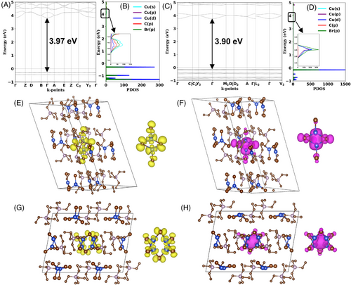
To gain insights into the PL mechanism and electronic structures, density functional theory (DFT) calculations have been carried out for (TEP)2Cu2Br4 and (TEP)2Cu4Br6. To calculate the accurate fundamental bandgaps for hybrid materials, HSE06 hybrid functional has been employed.[59] The valence bands consist of a series of flat bands in the band structures of (TEP)2Cu2Br4 and (TEP)2Cu4Br6 (Figure 3A,C), suggesting the presence of highly localized charge carriers. The calculated bandgap values are 3.97 eV and 3.90 eV for (TEP)2Cu2Br4 and (TEP)2Cu4Br6, respectively. The calculated projected density of states (PDOS) demonstrates that localized electronic states from [Cu2Br4]2− and [Cu4Br6]2− units contribute predominantly to both VBM and CBM of (TEP)2Cu2Br4 and (TEP)2Cu4Br6, respectively (Figure 3B,D and Figure S10). In both compounds, the VBM solely consists of Cu 3d and Br 4p orbitals, while Cu 4s and Br 4p antibonding orbitals dominate CBM. The orbital contribution of organic components is negligible in the band edges of these compounds, which is particularly true in the case of (TEP)2Cu4Br6. Moreover, the partial charge distribution density maps (Figure 3E–H) also demonstrate that electrons and holes are localized on discrete [Cu2Br4]2− and [Cu4Br6]2− anions. The contribution of inorganic units in the photophysical process of (TEP)2Cu2Br4 and (TEP)2Cu4Br6 was further validated by investigating the optimized ground state and excited state properties. As shown in Figures S11 and S12, both [Cu2Br4]2− and [Cu4Br6]2− inorganic units undergo large structural distortions in the excited state, demonstrated by the significant changes in bond lengths and angles. As a result of this structural distortion in the excited state, the Cu···Cu distances in the discrete inorganic units are shortened by ∼12% and 9% in (TEP)2Cu2Br4 and (TEP)2Cu4Br6, respectively, compared to the ground state. This is also evident in the partial charge density plot (Figure 3F,H), where electron clouds are mostly localized around the Cu atoms. The localized excitons and strong structural distortions are found to be significant in trapping the exciton, leading to the formation of highly stable STEs and strong electron–phonon coupling in these copper(I) halides. These self-trapped states result in midgap emission in (TEP)2Cu2Br4 and (TEP)2Cu4Br6 with calculated Stokes shift values of 0.33 and 0.64 eV, respectively (Table S8). The calculated emission energies of 2.92 and 2.76 eV for (TEP)2Cu2Br4 and (TEP)2Cu4Br6 are in reasonable agreement with the experimental values of 2.46 and 2.06 eV, respectively. The calculated results also agree with the experimental lower energy orange emission of (TEP)2Cu4Br6 compared to the greenish-white emission of (TEP)2Cu2Br4. The higher charge localization in the cluster centric [Cu4Br6]2− effectively reduces the energy of its STE state compared to [Cu2Br4]2−. The reduced effective mass calculation () of the exciton pair in (TEP)2Cu4Br6 is determined to be 1.6 times larger than that of (TEP)2Cu2Br4 (Table S8). This suggests that the former system has the potential for a higher radiative recombination rate, as supported by its higher measured PLQY value. The careful analysis of the experimental and theoretical results presented above validates the STE-originated bright emission in these two-hybrid copper(I) halides and illustrates their excited state configurational changes.[24, 27]
Based on our combined experimental and computational work, the following configuration coordinate diagram model is proposed for the broadband bright PL emission in (TEP)2Cu2Br4 and (TEP)2Cu4Br6 (Figure S13).[27, 50] Upon photoexcitation, electrons transition from the ground states of the inorganic copper(I) halide units to the excited state, where strong structural distortions occur. The structural distortion is accompanied by the relaxation of electrons from the singlet excited state to a low energy triplet STE state via intersystem crossing (ISC), aided by the strong electron–phonon coupling effect. Eventually, the radiative recombination of triplet STEs results in the observed large Stokes-shifted broadband ultrabright light emission in these hybrid copper(I) halides.
2.3 Stability
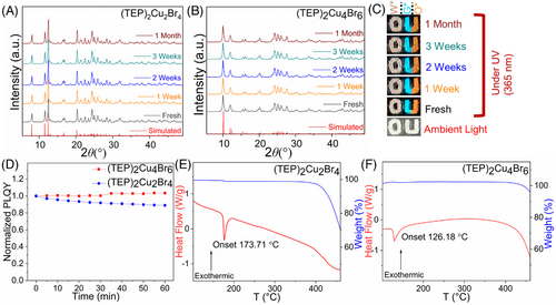
The highly efficient light emission of (TEP)2Cu2Br4 and (TEP)2Cu4Br6 are indicative of their potential for practical applications. For practical applications, it is important to ensure the stability of these compounds. Periodic PXRD measurements were performed on the as-synthesized samples of (TEP)2Cu2Br4 and (TEP)2Cu4Br6 for 30 days under ambient laboratory conditions (relative humidity of 30% and room temperature of 20°C). The unchanged PXRD data and visible light emission of the powder samples under UV exposure (see Figure 4A–C) suggest the improved air stability of these compounds. Moreover, both compounds demonstrate improved photostability with no significant loss of PLQY under 60 minutes of continuous irradiation of UV light at their PLEmax. It is evident from Figure 4D that (TEP)2Cu4Br6 has better photostability compared to (TEP)2Cu2Br4. Furthermore, (TEP)2Cu2Br4 and (TEP)2Cu4Br6 show markedly improved thermal stability with no significant weight loss up to 400°C, after which the compounds start to decompose (see Figure 4E,F). Interestingly it is noticeable that (TEP)2Cu2Br4 demonstrates higher thermal stability compared to the structurally similar ammonium copper halide (TEA)2Cu2Br4 which decomposes at 265°C (TEA = tetraethylammonium).[44] The larger size and greater nucleophilicity of phosphonium cations compared to the corresponding ammonium cations contributed to the improved thermal as well as overall stability of (TEP)2Cu2Br4, compared to (TEA)2Cu2Br4.[60] The silver analog, (TEP)3Ag6Br9, is also found to be stable with no weight loss up to 400°C (Figure S14). These results suggest the considerable improvements of air, thermal, and photo-stability of (TEP)2Cu2Br4 and (TEP)2Cu4Br6 compared to other luminescent inorganic and hybrid copper(I) halides such as Rb2CuX3, (TEA)2Cu2Br4, (TPA)CuX2, (TPA)2Cu4Br6, (TBA)CuX2 (X = Cl, Br), [ETPP]CuBr2, [ETPP]2Cu4Br6, (Bmpip)2Cu2Br4, etc.[25, 37, 39, 42, 44, 47, 49, 50] In combination, the ultrabright luminescence and improved stabilities make (TEP)2Cu2Br4 and (TEP)2Cu4Br6 potential candidates for practical optical applications.
2.4 Applications
2.4.1 Melt-processed thin films
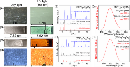
Interestingly, differential scanning calorimetry (DSC) measurements suggest endothermic thermal events at 173.71 and 126.18°C for (TEP)2Cu2Br4 and (TEP)2Cu4Br6, respectively. These thermal events correspond to their melting transitions with the formation of colorless liquids, confirmed by the melting point measurements. These observations were further supported by the reversible occurrences of these thermal events in the heating and cooling cycles of DSC, with no weight loss in thermogravimetric analysis (TGA) measurements within the 270°C range (see Figure S15). The small difference between these transitions of heating and cooling cycles is related to the heat capacity of the materials.[61] The sample purities before and after heating at 200°C were confirmed by the PXRD measurements (Figure S16). Subsequently, both compounds undergo photoluminescence on and off states under thermal simulation when they solidify and melt, respectively (see Figure S17). Moreover, the low-temperature congruent melting behavior of these hybrid copper(I) halides could be crucial for the melt-processing of these materials (e.g., as thin films). Obtaining thin films of 0D metal halides with uniform substrate surface coverage is challenging because of their ionic nature and well-separated 0D organic and inorganic structural units. Typically, thin film preparation for various hybrid metal halides involves solution processing, for example, spin-coating by dispersing polar solution or the polymer colloidal solution of the subject materials on a solid substrate surface.[38, 50, 62] For certain materials, solution deposition may have disadvantages, such as the lack of control of the crystal growth and poor substrate surface coverage or the interference of the polymer matrix in the optical properties of the subject materials. On the other hand, the melt-processability provides a toxic solvent-free, cost-effective alternative approach for thin film deposition.[63, 64] Moreover, this technique facilitates control over the size and orientation of the crystalline domains and thickness of the film.[65] Utilizing the congruent melting behavior of (TEP)2Cu2Br4 and (TEP)2Cu4Br6, uniform thin films with good coverages have been prepared by melting and pressing the molten liquids of their respective powder samples (approximately 50 mg) sandwiched between two microscopic slides (Figure 5A–D).[66, 67] A visual comparison of the thin films made by spin coating[38] and melt processing (see Figure 5A–D and Figure S18) suggests a better quality of films obtained through the latter method. Noteworthy, the as-prepared unoptimized melt-processed thin films showed identical XRD data and PL profiles as that obtained for (TEP)2Cu2Br4 and (TEP)2Cu4Br6 single crystals (Figure 5E–H). Further optimization of melt processing may have yielded even better results for potential practical applications,[68] such as enabling flexible and wearable optoelectronic devices.
2.4.2 Scintillation properties
The processing flexibility, improved stability, ultrabright luminescence with near-unity PLQY, and negligible self-absorption (due to the large Stokes shift values) of (TEP)2Cu2Br4 and (TEP)2Cu4Br6 motivated us to investigate their potential practical applications. In literature, several light-emitting metal halides have been reported as promising candidates for radiation detection applications, therefore, we first focused on radioluminescence (RL) and scintillation properties of (TEP)2Cu2Br4 and (TEP)2Cu4Br6. The absorption coefficients of (TEP)2Cu2Br4 and (TEP)2Cu4Br6 have been calculated for a broad range of photon energy from soft X-rays to high-energy gamma-rays and compared with other reported scintillator materials (based on the XCOM photon cross section database). The absorption coefficients of (TEP)2Cu2Br4 and (TEP)2Cu4Br6 are comparable with that of CdTe, CsPbBr3, MAPbBr3, (EDBE)PbCl4 and (TEA)2Cu2Br4, which indicate the potential attenuation capacity of these compounds for X-ray scintillation (see Figure 6A). It is noteworthy that hybrid organic–inorganic compounds deliver lower absorption to X-rays than all-inorganic materials due to the lack of heavy elements and lower material density. Here, although (TEP)2Cu2Br4 and (TEP)2Cu4Br6 have lower absorption than the commercial scintillator CdTe, they still deliver sufficient absorption compared to other reported metal halide scintillator materials. Single crystals of (TEP)2Cu2Br4 and (TEP)2Cu4Br6 exhibit bright greenish-white and orange emissions, respectively, under 30 kV (0.1 mA) X-ray irradiation corresponding to their RL emission spectra (see Figure 6B and Figure S19–S22). The broad emissions with peak positions at 519 nm and 622 nm are registered for (TEP)2Cu2Br4 and (TEP)2Cu4Br6, respectively. Notably, the RL emissions of both compounds appear at the same spectral region as their corresponding PL emissions at room temperature, suggesting an STE-based emission mechanism under X-ray irradiation.

High energy gamma (γ) photons (∼50 keV–10 MeV) are emitted from the decay of most radioactive isotopes. Low-cost, highly sensitive, and room-temperature solid-state gamma radiation detectors are in high demand for numerous applications in medicine, defense, and as well as in research.[69, 70] Therefore, the development of solution-grown hybrid organic–inorganic metal halides, in contrast to the all-inorganic scintillators, propelled great interest in this field.[71, 72] The noticeable absorption of (TEP)2Cu2Br4 and (TEP)2Cu4Br6 in the high energy gamma ray region (∼50 keV to 10 MeV) relative to the other above-mentioned scintillator materials (Figure 6A) inspired us to demonstrate their potential for gamma-ray detection. The absolute light output of 2800 photons/MeV and 15,800 photons/MeV were determined using the single photon technique from the pulse height spectra of (TEP)2Cu2Br4 and (TEP)2Cu4Br6 single crystals, respectively, excited with 662 keV γ-rays of 137Cs. The calculated energy resolution values from the photopeak of (TEP)2Cu2Br4 and (TEP)2Cu4Br6 are 13.2% and 10.9%, respectively. It must be noted that the maximum pulse shaping time of our setup is 10 µs for integration of the scintillation pulses. Considering the absence of the scintillation decay component(s) with a lifetime of less than 10 µs we can conclude that the observed light yield and energy resolution values are less than they would be in the case of integration time covering the whole decay curve. The room temperature light yields and energy resolution values reported here for (TEP)2Cu2Br4 and (TEP)2Cu4Br6 are comparable to that of the other hybrid perovskite-derived scintillator materials such as (C6H5(CH2)2NH3)2PbBr4 (10,000 photons/MeV), (EDBE)PbCl4 (9000 photons/MeV, EDBE = 2,2′-(ethylenedioxy)bis(ethylammonium), (BA)2PbBr4 (7000 photons/MeV, BA = butylammonium), MAPbI3 (< 1000 photons/MeV and 6.8%, MA), MAPbBr3 (< 1000 photons/MeV), and Gua3SbCl6 (1800 photons/MeV, Gua = N,N'-diphenylguanidinium).[72-76] However, note that direct comparisons of different scintillator materials have to be done with caution, as the results depend on many factors including applied X-ray irradiation energy, dose rate, radiation source and measurement techniques, etc.[43, 46, 77] Moreover, not many examples are available in the literature that reported energy spectra from γ-ray for hybrid scintillator materials.[71, 72, 78] Notwithstanding these issues, the experimentally measured scintillation properties suggest that (TEP)2Cu2Br4 and (TEP)2Cu4Br6 promising for X- and γ-rays scintillation applications.
2.4.3 Interconversion and information storage
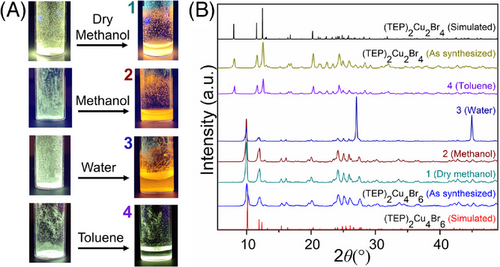
The identical chemical makeups (TEPBr and CuBr), but different compositions and crystal structures in (TEP)2Cu2Br4 and (TEP)2Cu4Br6 inspired us to investigate the possibility of structural transformations between the two compounds, which could enable their use as smart luminescent materials. Interestingly, the greenish-white emitting (TEP)2Cu2Br4 transformed to a bright orange emitter (under the irradiation of 365 nm UV light) immediately in contact with water (Video S1 and Figure 7). Consequently, the XRD patterns of the samples before and after soaking in water confirmed the transformation of (TEP)2Cu2Br4 to (TEP)2Cu4Br6 in the presence of water. Notably, this transformation was also observed in the presence of other polar solvents such as methanol (Video S2) and dry methanol. In the next step, we investigated the chemo-response of (TEP)2Cu2Br4 to relatively nonpolar solvents like toluene. Interestingly, as shown in Figure 7 and Video S3, (TEP)2Cu2Br4 retained its luminescence color and XRD pattern after soaking in toluene. To further shine a light on these phenomena, the response of precursor reagents, TEPBr and CuBr, with these solvents was tested. Noteworthy, CuBr is insoluble in all the solvents under the experiment, while TEPBr only dissolves in the solvents that facilitated the transformation of (TEP)2Cu2Br4 to (TEP)2Cu4Br6. These results suggest that the transformation only occurs when TEPBr can be released from (TEP)2Cu2Br4 in the presence of the solvent, depending on its solubility in that solvent and the process can be represented as the following Scheme 1.

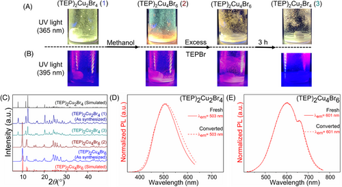
Based on these results, it is valid to assume that providing extra precursor organic salt (TEPBr) in the solution of (TEP)2Cu4Br6, may force its transformation back to (TEP)2Cu2Br4 by reverse crystallization. As a proof of concept, the PXRD and PL measurements have been performed before and after the addition of access to TEPBr. As shown in Figure 8A,B, the greenish-white color emission (1) of (TEP)2Cu2Br4 turned to orange color (2) by the addition of methanol and the PXRD pattern and PL spectra of the transformed sample (2) fitted well with the freshly prepared (TEP)2Cu4Br6 (Figure 8C,E). This bright orange emission color (2) starts to fade away after the addition of excess TEPBr in the solution and the greenish white emission (3) returns after stirring the resultant solution for 3 hours. Consequently, the PXRD pattern and PL spectra of the transformed sample (3) are in good agreement with the freshly prepared (TEP)2Cu2Br4 (Figure 8C,D). These observations confirm that (TEP)2Cu2Br4 and (TEP)2Cu4Br6 can undergo reversible interconversions along with their designated PL emission properties, by the stimulation of a suitable solvent or reverse crystallization. The complete interconversion can be represented as the following Scheme 2.

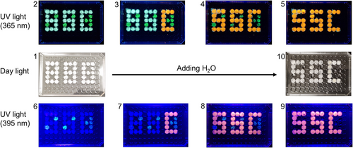
Remarkably, the unique interconvertible photoluminescence properties of these hybrid copper(I) halides open up a promising avenue for their potential applications in chemo-sensing, information storage, anti-counterfeiting, etc. As proof of concept, a three-digit encrypted pattern ‘888′ has been fabricated on a transparent plastic culture plate, with the powder samples of (TEP)2Cu2Br4 and a freshly made green-emitting hybrid manganese halide phosphor (based on TEP+). Figure 9 represents the pattern plate under daylight (1 and 10), 365 nm UV light (2–5), and 395 nm blue light (6–9). The as-fabricated pattern looks white under daylight (1), green under 365 nm UV light (2), and dark under 395 nm blue light (6). The blocks made of (TEP)2Cu2Br4 turned orange color (2–4 and 6–8) with the addition of water. Interestingly, the pattern plates 3 and 7 suggest that (TEP)2Cu2Br4 and (TEP)2Cu4Br6 can be used as two different phosphors to store information, where the code ‘C’ stands out only under 395 nm blue light. Finally, the green emission from manganese phosphor disappeared in contact with water and the well-defined stabilized orange secret pattern ‘SSC’ (5 and 9) (SSC = Solid State Chemistry) emerges. Based on this demonstration, low-cost and low toxicity (TEP)2Cu2Br4 and (TEP)2Cu4Br6-based effective encryption could be realized easily following permutation and combination strategy.
2.4.4 Anticounterfeiting and latent fingerprinting
(TEP)2Cu2Br4 and (TEP)2Cu4Br6 are versatile materials and demonstrate potential for other luminescent-based applications as well. Thus, luminescent inks based on both materials have been prepared by dispersing micron-size powder samples in toluene or polymer-based matrices. First, ‘OU’ graffiti has been drawn on different surfaces (glass slide, Teflon sheet, paper) and different background color papers (Figures S23–S25). Interestingly, both compounds showed distinguishable colors in all the cases in this experiment, suggesting the possibility of creating multicolor patterns on any color surfaces for anti-counterfeiting. In addition to their potential anti-counterfeiting applications, the as-prepared luminescent inks were used to demonstrate fingerprints (FPs) applications. The hybrid copper(I) halides studied in this work, have added advantages over other commonly used lead-based luminescent inks, due to their earth-abundant and low-toxicity elemental compositions.[28, 30, 79] As a proof of concept, a (TEP)2Cu2Br4 polymer ink-based FP has been deposited on black paper. Visualizing a high-resolution luminescent FP with the naked eye confirms the durability and affinity of this ink to the substrate surface (Figure 10A). The clear visualization of different latent features of FPs (LFPs) is essential for the reliable identification of individuals for various purposes, such as medical diagnosis, forensic investigations, control of access, and national security.[80-82] As shown in Figure 10A, high-level latent features, namely, island and pore that are essential for the identification of individuals, were easily identified in the (TEP)2Cu2Br4 ink-based FP.[80, 83] These results suggest the high reliability and sensitivity of (TEP)2Cu2Br4-based luminescent ink for LFP visualization and detection.

2.4.5 Phosphor for LEDs
Yet another potential application of luminescent metal halides is their use as phosphors in solid-state lighting, including white light emitting diodes (WLEDs) and displays. The well-known methods to construct WLEDs require fabricating the LED chips with multiple layers of blue, yellow, and red phosphors in a particular ratio to cover the entire region of the visible light spectrum.[84, 85] The efficient broadband greenish-white and orange-red emissions from (TEP)2Cu2Br4 and (TEP)2Cu4Br6 phosphors that are prepared using the same starting materials make them promising candidates for the construction of WLEDs. Moreover, their earth-abundant, low-cost, and low-toxicity elemental compositions are advantageous as compared to the traditional rare-earth metal-based phosphors for lighting applications.[28, 30, 84-86] As a proof of concept, (TEP)2Cu2Br4 and (TEP)2Cu4Br6-based UV-pumped LEDs have been fabricated to demonstrate their suitability for solid-state lighting. Interestingly, distinguishable cool white and warm white luminous emission can be realized by coating (TEP)2Cu2Br4 and (TEP)2Cu4Br6 luminescent inks, respectively, on commercial UV LED chips (365 nm) (see insets in Figure 10B,C). The calculated spectral parameters of the fabricated phosphor-converted (pc)-LEDs are shown in Table S9. Subsequently, a color rendering index (CRI) value of 67 and CIE value of (0.26, 0.36) have been calculated for (TEP)2Cu2Br4-based LED. The broadband orange emission of (TEP)2Cu4Br6 allows the fabrication of warm white LED with a much higher CRI value of 80 and lower correlated color temperature (CCT) of 2382 K than the widely used fluorescent bulbs (∼72 and 3000 K) in the market, suggesting its potential for indoor lighting applications.[85, 87] As shown in Figure 10B, the emission spectra of both pc-LEDs cover the wide range of the visible spectrum, suggesting their potential for the construction of WLEDs with neutral white light chromaticity and high color purity.[84, 86] Further optimization of WLEDs is possible through the addition of secondary phosphors, adjusting proportions of both phosphors, and device engineering. For instance, the inset of Figure 10C shows a photograph of the powder samples of both hybrid copper(I) halides, where the letters “C” and “u” represent two single phosphors and “X” represents the white color emission from the mixture of both phosphors. All these above results demonstrate that (TEP)2Cu2Br4 and (TEP)2Cu4Br6 have excellent potential for solid-state lighting applications.
3 CONCLUSION
In summary, this work reports the synthesis and optical characterization of three hybrid metal halides (TEP)2Cu2Br4, (TEP)2Cu4Br6, and (TEP)3Ag6Br9. (TEP)3Ag6Br9 possesses a 1D crystal structure and demonstrates very weak PL emission with a similar profile to that of the organic precursor salt TEPBr. In contrast, (TEP)2Cu2Br4 and (TEP)2Cu4Br6 demonstrate distinct 0D crystal structures containing [Cu2Br4]2− and [Cu4Br6]2− inorganic anionic units, respectively. The strong quantum confinement effect in the molecular structures of (TEP)2Cu2Br4 and (TEP)2Cu4Br6 and negligible self-absorption result in their ultrabright greenish-white and orange emissions, respectively, with near unity PLQY for both compounds. In addition, efficient radioluminescence is observed under both X- and γ-rays irradiation, suggesting the potential of (TEP)2Cu2Br4 and (TEP)2Cu4Br6 for scintillation applications. Considering the high atomic concentration of hydrogen in these compounds (60 at. % and 55 at. % for (TEP)2Cu2Br4 and (TEP)2Cu4Br6, respectively), these compounds may also be interesting for application in fast neutron threshold detectors. Based on our combined optical (PL and RL) spectroscopy and computational studies, photoemission in (TEP)2Cu2Br4 and (TEP)2Cu4Br6 is attributed to STEs localized on the copper-halide molecular units, distortions of which upon photoexcitation determines the Stokes shift values for each compound.
(TEP)2Cu2Br4 and (TEP)2Cu4Br6 demonstrate improved air-, thermal- and photo-stability, which in combination with their outstanding optical properties, make them candidates for several practical applications. In this work, we demonstrated the interconversion and reversible luminescence on-off switching for (TEP)2Cu2Br4 and (TEP)2Cu4Br6, with the aid of external chemical and thermal stimuli, which can be realized for sensing, high-level security, information storage, and anticounterfeiting applications. Furthermore, proof-of-concept demonstrations of the use of these materials in security screening and solid-state lighting yielded promising results. This work shows that low-dimensional Cu(I) halides have remarkable structural diversity and intricate details of individual structures impact their photophysical properties. Additional work in the field with the aim of an in-depth understanding of the structure-property relationships in this materials class will provide rational materials design ideas for the preparation of low-cost and environmentally friendly copper(I)-based multifunctional smart materials for next-generation practical applications.
4 EXPERIMENTAL SECTION
4.1 Materials
Copper(I) bromide (> 99%, Alfa Aesar), silver bromide (99%, Alfa Aesar), TEP bromide (TEPBr) (> 98%, TCI), N,N-dimethylformamide (DMF) (anhydrous, Sigma-Aldrich), hypophosphorous acid (50 wt%, Alfa Aesar) were purchased and used as received with no further purification. Reactions containing silver reagents were performed by wrapping the glass scintillation reaction vials with aluminum foil. All syntheses procedures were carried out in a nitrogen-filled glovebox unless otherwise stated.
4.2 (TEP)2Cu2Br4 synthesis
A mixture of 0.454 g (2.00 mmol) of TEPBr and 0.287 g (2.00 mmol) of copper(I) bromide were dissolved in 1.5 mL of DMF (anhydrous) at room temperature of 20°C to form a clear colorless precursor solution in a nitrogen-filled glovebox. The solvent was slowly evaporated at room temperature over a 5-day period and up to 2.0 cm long colorless block crystals of (TEP)2Cu2Br4 were collected. The crystals were stored in a nitrogen-filled glovebox for further optical characterizations.
4.3 (TEP)2Cu4Br6 synthesis
A mixture of 0.454 g (2.00 mmol) of TEPBr and 0.574 g (4.00 mmol) of copper(I) bromide were dissolved in 1.5 mL of DMF (anhydrous) at room temperature of 20°C to form a clear yellowish precursor solution in a nitrogen-filled glovebox. The solvent was slowly evaporated at room temperature over a 5-day period and up to 1.0 cm long colorless block crystals of (TEP)2Cu4Br6 were collected. The crystals were stored in a nitrogen-filled glovebox for further optical characterizations.
4.4 (TEP)3Ag6Br9 synthesis
A mixture of 0.114 g (0.500 mmol) of TEPBr and 0.093 g (0.500 mmol) of silver bromide was dissolved in 3.5 mL DMF (anhydrous) at 80°C to form a clear colorless precursor solution. The solvent was slowly evaporated at 40°C over a 3-day period and up to 0.3 cm long colorless block crystals were collected and stored in ambient air.
4.5 Preparation of luminescent inks using (TEP)2Cu2Br4 and (TEP)2Cu4Br6
Two grams of polymethylmethacrylate (PMMA) were added to 6 mL of toluene and stirred at room temperature until PMMA was completely dissolved. Solution-grown single crystals of the title compounds were ground into a microcrystalline powder sample, from which 300 mg was used for the ink preparation; the powder sample was dispersed into the PMMA solution by stirring for 1 day. This luminescent ink was used for printing latent FPs, graffiti, and coating commercial UV LED chips to fabricate white light-emitting diodes.
4.6 PXRD measurements
PXRD measurements were carried out at room temperature for polycrystalline samples using a Rigaku MiniFlex600 system equipped with a Ni-filtered Cu Kα radiation source. PXRD scans were performed in the 3–90° (2θ) range with a step of 0.02°, and the XRD patterns were analyzed using a PDXL2 software package. To test the air-stability of the named materials, powder samples were left on a laboratory bench under ambient air conditions (20°C and 30% relative humidity) for 30 days during which periodic PXRD measurements were performed.
4.7 SCXRD measurements
SCXRD measurements were performed using a Bruker D8 Quest Kappa-geometry diffractometer with an Incoatec Iµs microfocus Mo K X-ray source and a Photon II area detector. The data were corrected for absorption using the semi-empirical method based on equivalent reflections, and crystal structures were solved by intrinsic phasing methods as embedded in the APEX3 v2015.5-2 program. Site occupancy factors were checked by freeing occupancies of each unique crystallographic position. Details of the data collection and crystallographic parameters are given in Table S1. Atomic coordinates, equivalent isotropic displacement parameters, selected interatomic distances, and bond angles are provided in Tables S2–S5. CCDC 2312764–7312765 contains the supplementary crystallographic data for this paper. These data can be obtained free of charge from The Cambridge Crystallographic Data Centre via www.ccdc.cam.ac.uk/data_request/cif.
4.8 TGA/DSC measurements
Simultaneous TGA/DSC were measured on ∼10 mg single crystal samples of the respective title compounds on a TA Instruments SDT 650 thermal analyzer system. Crystals were heated up from 25 to 475°C under an inert nitrogen gas flow at a rate of 100 mL/min, with a heating rate of 5°C/min.
4.9 PL measurements
Room-temperature PL emission and PLE measurements were carried out on single crystal samples of the respective title compounds using HORIBA Jobin Yvon Fluorolog-3 spectrofluorometer with Xenon lamp source and Quanta- integrating sphere. Data were collected using the two-curve method in a varied range from 250 to 750 nm. The Commission Internationale de l'Eclairage (CIE) color plots were generated using GoCIE software. For the photostability measurement, the single crystals of the respective title compound were placed inside the Quanta-φ integrating sphere on the Jobin Yvon Fluorolog-3 spectrofluorometer. The sample was then exposed to the full power of the Xenon lamp at its PL excitation maximum wavelength. Periodic PLQY measurements were taken every 5 min under these conditions for a total of 60 minutes.
4.10 Diffuse reflectance measurements
UV-vis diffuse reflectance data were collected on powder samples of the title compounds using a PerkinElmer Lambda 750 UV-vis-near-infrared spectrometer with a 100 mm Spectralon InGaAs Integrating Sphere over a range of 250–1100 nm. Diffuse reflectance data were then transformed to pseudo-absorption spectra utilizing the Kubelka-Munk function , where is the absorption coefficient, S is the scattering coefficient, and R is the reflectance.
4.11 Radioluminescence measurements
The approximate sizes of the investigated crystals of (TEP)2Cu2Br4 and (TEP)2Cu4Br6 are ∼ 2×2×10 mm3 and 4×4×2 mm3, respectively. Samples were submerged in mineral oil to limit moisture exposure. Room-temperature radioluminescence (RL) measurements were done under continuous 30 kV (0.1 mA) X-ray irradiation using a CMX003 X-ray generator. The emission spectra were recorded in reflection geometry using a 150 mm focal length monochromator over a wavelength range of 200 to 900 nm. The pulse height of the samples with 137Cs sealed sources was collected for light yield measurements using a standard Hamamatsu R2059 photomultiplier tube (PMT) connected to Canberra 2005 pre-amplifier, Ortec 672 spectroscopy amplifier, and a Tukan 8K multichannel analyzer. The Hamamatsu R6231-100 super bialkali PMT was used for energy resolution measurements. The oil-filled container was Teflon-wrapped and mated to the PMT. The energy resolution was calculated from the ratio of the full width at half maximum of the photopeak to its centroid (ER): ER = ΔE(FWHM)/E. A maximum pulse shaping time of 10µs was used to ensure complete integration of the scintillation pulses. The absolute light yield in photons per MeV (photons/MeV) was measured via the single photoelectron technique using a factory-measured quantum efficiency PMT. The Hamamatsu H3177-50 PMT coupled to the NI USB 6009 data acquisitor with a sampling rate of 4000 Hz was used for afterglow measurements. The sample in the oil-filled container was mounted in front of the PMT. After 10-sec irradiation of the sample with a CMX003 X-ray generator (35 KeV, 0.1 mA), the X-ray was turned off and the afterglow was registered.
4.12 DFT calculations
The DFT computations were carried out using the Vienna Ab-initio Simulation Package software with the projector-augmented-wave method.[88-92] The exchange-correlation is treated using the Perdew-Burke-Ernzerhof (PBE) functional within the generalized gradient approximation.[93] For (TEP)2Cu4Br6, four crystallographic disordered Cu atoms are removed manually, and the remaining four Cu atoms are assigned to unity occupancy, and the resultant model is used in the present work. A kinetic energy cutoff of 500 eV is used to generate a plane-wave basis set. For Brillouin Zone sampling a 2×3×2, and 3×3×2 gamma-centered k-points mesh is used for (TEP)2Cu2Br4, and (TEP)2Cu4Br6, respectively. The lattice parameters were held constant at experimentally measured values. For the geometry optimization, the threshold criteria for self-consistent field (SCF) energies and the residual forces on each atom are set as eV and 0.02 eV , respectively. To accurately determine the bandgap values, hybrid Heyd-Scuseria-Ernzerhof 2006 (HSE06)[94] functional with 25% Hartree-Fock exact exchange ( was employed.
We employed the widely used ΔSCF method to assess the excited state properties.[95] This method involves manually altering the electron occupancy of specific energy bands to mimic the transition to an excited state. To illustrate charge localization, a supercell was created by repeating the unit cells twice in both the x and y directions. In line with the Franck-Condon principle, the energy differences between the excited and ground states were calculated to determine optical excitation and emission energies. However, optimizing the supercell for both ground and excited states using the HSE06 functional presents computational challenges. Therefore, we opt for the more cost-effective hybrid PBE0 functional.[96] To better account for long-range electron-electron interactions, and to keep all the calculations on equal footing, a one-step HSE06 calculation was performed, following the PBE0 optimization. The range-separated nature of the HSE06 functional makes it particularly suitable for properties like bandgap and excitation energy in extended systems.[97]
ACKNOWLEDGMENTS
This work was supported by the National Science Foundation (NSF DMR-2045490). We thank Dr. Douglas Powel for the help with SCXRD measurements (supported by NSF grant CHE-1726630). Computational work (Yashpal Singh, John M. Lane, and Neeraj Rai) was supported by the NSF under Grant No. 1757220. This work used Stampede 2 at Texas Advanced Supercomputing Center (TACC) through allocation CHE140141 from the Advanced Cyberinfrastructure Coordination Ecosystem: Services & Support (ACCESS) program,[98] which is supported by National Science Foundation grants #2138259, #2138286, #2138307, #2137603, and #2138296. Part of this work was performed on computational resources at HPC2 (High-Performance Computing Collaboratory) at Mississippi State University. Financial support was provided by the University of Oklahoma Libraries' Open Access Fund.
CONFLICT OF INTEREST STATEMENT
The authors declare no conflicts of interest.
Open Research
DATA AVAILABILITY STATEMENT
The data that support the findings of this study are available from the corresponding author upon reasonable request.


