Optimized Design and Implementation of CRYSTALS-KYBER Based on MLWE
Abstract
CRYSTALS-KYBER is a postquantum key exchange mechanism based on the MLWE problem. At present, it is a major challenge to realize CRYSTALS-KYBER with high-performance and low-resource consumption on the FPGA platform. The design proposed in this paper aims at the high efficiency implementation of CRYSTALS-KYBER based on the MLWE scheme. In this work, multipath delay commutator–number theoretic transform (MDC-NTT) and area-optimized hash unit are employed to optimize the overhead and clock cycle occupancy of the whole implementation. The CRYSTALS-KYBER public-key encapsulation circuit requires only 5551 clock cycles to execute, reducing the latency by 38.9% compared to the best existing iteration NTT designs and improving hardware efficiency by 1.6–1.9 times. The maximum operating frequency also reaches up to 225 MHz.
1. Introduction
With the rapid development of information technology and the internet, ensuring the security and confidentiality of information transmission has always been a key issue in the field of information technology. In current cryptographic systems, classical public-key cryptographic algorithms such as RSA [1] and elliptic curve cryptography (ECC) [2] are mainly used. However, in 1994, Peter Shor proposed an algorithm that can factorize integers in polynomial time [3]. It can be run on a quantum computer, posing a serious threat to current traditional cryptography. Two solutions have been proposed: postquantum cryptography (PQC) and quantum cryptography. PQC is a new standard for classical cryptographic algorithms, while quantum cryptography utilizes the properties of quantum mechanics to protect data. Both schemes may have a place in future cryptographic systems, but their algorithm principles are fundamentally different. As a current research hot spot, PQC is similar to the cryptographic algorithms we currently study. Based on difficult mathematical problems, POC schemes avoid being as vulnerable to quantum attacks as traditional algorithms, such as integer factorization [4] and discrete logarithm algorithms [5].
The National Institute of Standards and Technology (NIST) in the United States began researching PQC in 2012 and initiated the largest and most influential cryptographic standardization competition to date. After nearly 11 years, on August 24, 2023, NIST officially published draft standards for three algorithms: CRYSTALS-KYBER, now renamed ML-KEM for general encryption, CRYSTALS-Dilithium, now renamed ML-DSA for digital signatures, and SPHINCS+, now renamed SLH-DSA for alternative digital signatures. Among them, the lattice-based CRYSTALS-KYBER has received widespread approval due to its strong resistance, simplicity, high efficiency, and suitability for building complex applications. It is recognized as the most promising category of PQC schemes. Although the new draft simplifies some hash operations from the original protocol for security purposes and adds input validation, the overall architecture remains largely unchanged. Therefore, this paper still focuses on architecture design and optimization based on the Kyber protocol, which remains highly relevant to the overall design of the new draft.
Lattice-based cryptographic schemes can be divided into key encapsulation mechanisms (KEMs) and digital signatures in terms of functionality, or divided into learning with errors (LWE), ring learning with errors (RLWE), module learning with errors (MLWE), NTRU, etc., in terms of the underlying difficult problems. As the main research object of this paper, CRYSTALS-KYBER is a KEM scheme based on MLWE in the lattice cryptographic difficult problem. As it is easiness of implementation on hardware platforms, it has been a focal point of research in the field of cryptography.
- a.
Optimization design of the core operator NTT: We propose two NTT architectures based on MDC pipelining and iterative methods and optimize them for latency and data access methods. We solve the problem of cycle redundancy in polynomial and BF operations while improving the maximum operating frequency and data throughput of the overall architecture.
- b.
Optimization design of the sampler based on hash functions: We optimize the hash instantiation functions used in the CRYSTALS-KYBER protocol, such as XOF and SHAKE. By simplifying parameter design and reducing critical paths, we reduce resource consumption while significantly improving the maximum operating frequency.
This paper completes KYBER.CCAKEM hardware optimization design of CRYSTALS-KYBER based on FPGA Artix-7 XC7a35T. The implemented design has advantages such as high throughput, low latency, and moderate resource consumption compared to current mainstream designs.
2. Preliminaries
2.1. Lattice Theoretical Basis and MLWE Problem
The set of vectors b1, b2, b3, …, bn is called a lattice basis, where the coefficients xi belong to the set of integers Z, that is, ∈ Z. The number of vectors in the lattice basis is the dimension of the lattice, and while the lattice basis is not unique, the dimension remains constant. In the field of cryptography, the lattice is characterized by an infinite set of periodically structured points arranged in a regular pattern in an n-dimensional Euclidean space. All lattice points can be formed by different lattice bases, and lattice bases can be transformed into each other through linear transformations.
The definition of a lattice gives rise to two fundamental mathematical problems: the shortest vector problem (SVP) and the closest vector problem (CVP). These problems can further lead to variations such as the approximate shortest vector problem (ASVP) decision version and the shortest linearly independent vector problem (SLIVP). All of these are mathematically challenging problems in the theory of lattices. In the context of PQC, LBC such as LWE, RLWE, and MLWE can be constructed based on the underlying mathematical problems that are hard on average. These problems provide resistance against quantum attacks, while the algorithms are efficient and easy to implement.
RLWE Problem: Let Rq be a ring polynomial with q being a prime number and n being an integer. Consider a polynomial a ∈ Rq and a⟵U, an error polynomial e ∈ Rq and e ⟵ Dσ.
The goal is to find a polynomial s ∈ Rq such that the equation b = αs + e holds.
MLWE Problem: Given a matrix A ∈ , where the polynomials in A are chosen uniformly at random, and an error polynomial vector e ∈ , where the elements in e follow the distribution , the goal is to find a polynomial vector s such that the equation b = As + e holds, where b ∈ is a known polynomial vector.
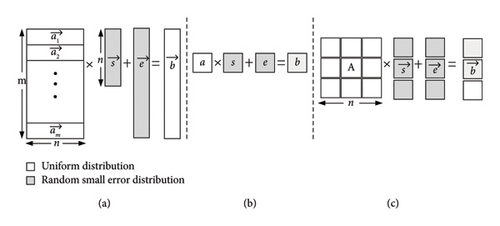
The difference between MLWE and RLWE or LWE lies in the dimensionality of variables and parameters. The specific design process of the MLWE scheme is shown in Algorithm 1 in the official documentation, where the relationship between the private key and the public key is defined as t = As + e. In practical designs, to save clock cycles and simplify circuit structures, a set of data satisfying uniform distribution in the range of [0, q − 1] can be pregenerated and stored as public and private keys in read only memory (ROM). The security of the MLWE public-key encapsulation scheme mainly relies on the random errors introduced into the public key and ciphertext. However, as the security level increases, the size of the ROM storing the keys needs to be increased, and the required bandwidth for transmission also needs to be increased as well. Therefore, MLWE introduces an important parameter k to limit the dimension of the public-key matrix, making the dimensions of the matrix A k × k, typically set as k = 2, 3, or 4. The highest degree of the polynomial is set to 256. In LBC schemes based on the LWE problem, the complexity of the operations depends on the underlying mathematical problem. It is difficult to judge the complexity of a cryptosystem based solely on its theoretical definition. However, Figure 1 provides a visual representation of the differences in computational characteristics between LWE, RLWE, and MLWE. These schemes generally have similar sampling methods, with the public-key components following a uniform distribution and the error perturbation terms following some random small distribution such as Gaussian or centered binomial distribution. However, the main factor influencing their performance is the complexity of the underlying mathematical operations.
-
Algorithm 1: M-LWE encryption.
-
Input: Public Key: A ← U and t; Private Key:
-
Plaintext: m ← {0, 1}n
-
Output: Ciphertext: u, v; Decrypted plaintext: m′
- 1.
Sampling: e1, ; e2 ← βη
- 2.
Plaintext Encode:
- 3.
Calculating ciphertext: u = ATr + e1,
- 4.
Decryption: c = v − sTu
- 5.
Decrypted plaintext: m′ = decode(c)
- 6.
returnu, v, m′
In Figure 1, each small square represents an individual polynomial, with gray squares representing random small error distributions and white squares representing uniform distributions. In the case of LWE, the core operation is the multiplication and addition operations between matrices. RLWE involves polynomial multiplication in a ring, while MLWE combines the computational characteristics of both LWE and RLWE, involving low-degree matrix and vector polynomial multiplication operations.
In terms of complexity, LWE has the highest complexity, followed by MLWE, and RLWE has the lowest complexity. The security level follows a similar pattern.
2.2. Composition and Analysis of the CRYSTALS-KYBER Protocol Based on MLWE
Following three rounds of evaluation, in July 2022, NIST chose three LBC algorithms, namely, CRYSTALS-CRYSTALS-KYBER (KEM), CRYSTALS-Dilithium (Digital Signatures), FALCON (Digital Signatures), and one hash-based algorithm SPHINCS+ (digital signatures) as the initial four quantum-resistant cryptographic algorithms [18]. The security of CRYSTALS-KYBER is based on the MLWE problem, and the performance/security trade-off can be directly adjusted by tuning the size of the matrix k and the noise parameter η, making it suitable for most applications. Therefore, it is necessary to conduct research on the deployment of CRYSTALS-KYBER in advance.
The construction of CRYSTALS-KYBER follows two stages: First, a PKE scheme with a CPA security level is constructed, and then, a secure KEM scheme is constructed using the Fujisaki–Okamoto transformation [19], which includes a PKE scheme for encrypting fixed-length messages of 32 bytes. This paper mainly analyzes the algorithm of KYBER.CCAKEM and studies its hardware implementation. KYBER.CPAPKE mainly includes three steps: key generation (KYBER.CPAPKE.KeyGen), plaintext encryption (KYBER.CPAPKE.Enc), and ciphertext decryption (KYBER.CPAPKE.Dec) [17]. KEM consists of PKE, both of which involve three steps. The main difference between them is that KEM’s encapsulation includes PKE’s encryption and decryption. To simplify the notation, B denotes the set of 8-bit unsigned integers (Byte), “” denotes data in the NTT domain, and “°” denotes the coefficient-wise multiplication of two polynomials of vectors or matrices in the NTT domain. The algorithms and procedures for KYBER.CPAPKE are shown in Algorithms 2, 3, and 4. The specific procedures for KYBER.CCAKEM are shown in Algorithms 5, 6, and 7.
-
Algorithm 2: KYBER.CPAPKE.KeyGen (ρ, σ).
-
Input: Random number of seeds: (ρ, σ)
-
Output:
- 1.
- 2.
- 3.
- 4.
- 5.
- 6.
- 7.
- 8.
returnpk, sk
-
Algorithm 3: KYBER.CPAPKE.Enc (pk, m, r).
-
Input: Public Key: ; Plaintext:
-
Random number of seeds:
-
Output: Ciphertext:
- 1.
- 2.
- 3.
- 4.
- 5.
- 6.
Decompressq(Decode1(m), 1)
- 7.
- 8.
- 9.
returnc = c1∥c2
-
Algorithm 4: KYBER.CPAPKE.Dec (sk, c).
-
Input: Secret Key:
-
Ciphertext:
-
Output: Delayed plaintext:
- 1.
- 2.
- 3.
- 4.
- 5.
returnm
-
Algorithm 5: KYBER.CCAKEM.KeyGen().
-
Output: Public key
-
Output: Secret key
- 1.
- 2.
(pk, sk′)≔KYBER.CPAPKE.KeyGen( )
- 3.
sk≔(sk′‖pk‖H(pk)‖z)
- 4.
return(pk, sk)
-
Algorithm 6: KYBER.CCAKEM.Enc (pk).
-
Input: Public key pk ∈ B12·k·n/8+32
-
Output: Ciphertext
-
Shared key K ∈ B∗
- 1.
m ← B32
- 2.
m ← H(m)
- 3.
(K, r)≔G(m‖H(pk))
- 4.
c≔KYBER.CPAPKE.Enc(pk, m, r)
- 5.
- 6.
return(c, K)
-
Algorithm 7: KYBER.CCAKEM.Dec (c, sk).
-
Input: Ciphertext
-
Secret key
-
Output: Shared key
- 1.
- 2.
- 3.
z≔sk + 24·k·n/8 + 64
- 4.
m′≔KYBER.CPAPKE.Dec(s, (u, v))
- 5.
- 6.
c′≔KYBER.CPAPKE.Enc(pk, m′, r′)
- 7.
ifc = c′then
- 8.
- 9.
else
- 10.
K≔KDF(z‖H(c))
- 11.
end if
- 12.
returnK
The CRYSTALS-KYBER algorithm is an efficient and flexible PQC scheme that directly incorporates the NTT function to reduce the computational complexity of polynomial multiplication in the core module. By adjusting the parameters, it allows for increased dimensions of polynomial matrices and vectors without modifying the underlying algorithm, thus achieving flexible and reliable security.
Different application scenarios have different requirements for security levels and resource overheads. In this paper, considering that k = 2 already satisfies most security needs, the sizes of ciphertexts, public keys, and private keys directly impact the system’s storage space and execution clock cycles, without significantly affecting the core modules and overall architecture. Therefore, this paper focuses on the hardware implementation of KYBER-512, which can be extended to higher security levels by modifying the control unit and increasing memory resources.
3. Design and Optimization of Core Submodules of CRYSTALS-KYBER Protocol
Based on the introduction of protocols and algorithms in the previous text, the CRYSTALS-KYBER protocol can be understood as a proven MLWE lattice cipher scheme with the public key in the NTT domain, encryption, and decryption completed in the time domain by hash function encapsulation. Therefore, when designing the lattice cipher hardware based on CRYSTALS-KYBER protocol, this paper proposes a sampling module based on a hash function, MDC pipeline NTT and iterative NTT, and some functional submodules to optimize the overall design from the module.
3.1. Public Key/Noise Sampler Based on Hash Function
The CRYSTALS-KYBER algorithm utilizes the CRYSTALS-KYBER protocol [17] to achieve public-key encapsulation. In this algorithm, public-key encapsulation is primarily accomplished by utilizing the SHA3-256, SHA3-512 hash function, and the output expandable functions SHAKE-128 and SHAKE-256 to generate pseudorandom bit sequences. The SHA3-256 and SHA3-512 hash functions can, respectively, produce 256-bit and 512-bit hash values for message inputs of any length. On the other hand, SHAKE-128 and SHAKE-256 are extension functions of SHA3 that can generate hash values of variable lengths as needed. The flexibility of setting the output width makes the SHAKE function suitable for use as a pseudorandom number generator (PRNG). When implemented in hardware, both the SHA3 and SHAKE functions employ the same Keccak module but with different input and output widths based on the hash standard rules.
The Keccak module utilizes a sponge structure and involves three main operations: message padding, message absorption, and message squeezing. The message padding rule involves adding “10 × 1” padding to the message after simple preprocessing. This is achieved by appending a “1” bit at the end of the message, followed by multiple “0” bits, and then appending another “1” bit. For SHA3 series functions, the preprocessing method concatenates two bits of binary “01” after the message. For SHAKE functions, four bits of binary “1111” are concatenated after the message. The number of added “0” bits is determined by the length of the message to ensure that the length of the padded message is a multiple of the message block length, denoted as “r.” The padded message is then split into multiple message blocks based on the block length to undergo message absorption and squeezing. In both message absorption and squeezing, the iteration function “f” is used to absorb and process the split message blocks multiple times. In the message squeezing stage, if the length of the desired hash value “d” is less than the block length, the high “d” bits of the last output are directly taken as the message digest. Otherwise, the iteration function is called again to squeeze and concatenate the high “r” bits of each output until the required length is achieved.
It is important to note that the hash functions employed in the CRYSTALS-KYBER protocol do not require iteration in the squeezing stage. The entire sponge structure process can be represented by the function SPONGE [f, pad, r] (N, d), and the iteration function “f” is separately represented by Keccak-p[b, nr]. The internal structure of the iteration function is illustrated in Figure 2.
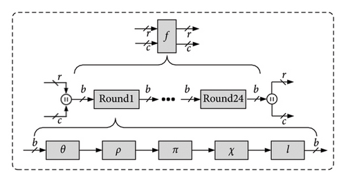
In the CRYSTALS-KYBER protocol’s public-key encapsulation circuit, the SHA3 module plays a role as a sampling function module rather than being the main module that affects performance. To optimize the area while maintaining overall frequency, the SHA3 module stores the 64-bit constants RC as 7-bit values. This reduces resource overhead without altering the logical functionality of the circuit. The iteration function in the SHA3 module is implemented using pure combinational logic and completes one iteration every 24 cycles. Consequently, the SHA3 module can provide up to 1344 bits of pseudorandom numbers every 24 cycles.
The SHA3-256, SHA3-512, SHAKE-128, and SHAKE-256 functions are essentially different parameterizations of the Keccak function, corresponding to H(), G(), XOF(), and PRF() in the protocol, respectively. In this protocol, the SHA3-512 function generates a 32-byte seed for SHAKE-128 and SHAKE-256. SHAKE-128 is responsible for generating random numbers for the rejection sampling module of the public-key matrix A. On the other hand, SHAKE-256 provides random numbers of various lengths for sampling the random and error terms according to a binomial distribution. When rejecting samples through XOF to obtain the values of 256 coefficients of a polynomial in matrix A, 384 bytes are required, which equals 256 × 12 bits. One round of XOF can generate 1344 bits or 168 bytes. Since rejecting samples discards data greater than q, redundant sampling is performed here, requiring at least 4 rounds of XOF (based on multiple experiments, 4 rounds generally meet the requirements) until all 256 coefficients of this polynomial are obtained. As for the PRF function, the effective number of output bits per round is 1088 bits or 136 bytes. Therefore, at most two iterations (i.e. η = 3) are needed to obtain all the data required for sampling. Based on hash function–based random binomial distribution sampling using a comparison of Hamming distance differences, setting the sampler to 8, and compatible with noise parameters of 2 and 3, ensuring that 8 data points can be sampled in each cycle. Generating a 256-term polynomial only requires 64 cycles. By reducing the bit storage for RC and integrating all instantiated hash functions into a single module controlled by the mod signal, the design improves compactness and versatility, resulting in significant area reduction compared to other designs.
3.2. Polynomial Multiplication NTT Optimization Design
The NTT module is the most critical computational module in the overall hardware implementation of CRYSTALS-KYBER. It is used to perform complex operations for polynomial multiplication in the matrix. CRYSTALS-KYBER-512 is a specific instance of the CRYSTALS-KYBER protocol, which is a parameter set based on the MLWE problem. The protocol directly applies the decomposition of the polynomial multiplication module into NTT forward and inverse transform modules. In the key generation phase, vectors require four NTT computations of 256 points each. In the plaintext encryption phase, two NTT transformations of 256 points each and three inverse NTT (INTT) transformations are required. In the ciphertext decryption phase, two NTT computations and one INTT computation are needed.
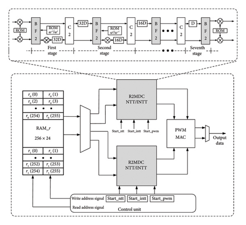
This article presents the design of a MDC pipelined NTT architecture, as shown in Figure 3, to accelerate the NTT computation in Algorithm 8 and handle complex memory access during the computation process. The MDC-NTT hardware circuit adopts two input paths, with data points on the two paths decreasing by level in each stage of the pipelined input. By making the BF unit configurable, the design allows the use of Cooley–Tukey (CT) units during NTT execution and Gentleman–Sande (GS) units during INTT execution. This approach eliminates the need for data preprocessing and postprocessing, as well as the need for a bit-reversal (BR) unit, streamlining the overall architecture. Both forward and inverse transforms use two multiplication units to process the two inputs in the same clock cycle, dividing the two input data streams into 7 levels of automatic serial pipeline operation according to NTT computation rules, which eventually help reducing input data delay and total computation cycle.
-
Algorithm 8:q = 3329 NTT polynomial multiplication.
-
Input: k-dimensional vector polynomial: rk ∈ Rq, 256 primitive roots: φi (0 < i < n), Highest degree term of a polynomial: n
-
Output: The value of n points on the NTT field
- 1.
for i = 0: n − 1 do
- 2.
r[i] = r[i]·ϕi
- 3.
endfor
- 4.
for s = 0: (log2 n) − 1 do
- 5.
for k = 0: 2s − 1 do
- 6.
for j = 0: n/(2s − 1) − 1 do
- 7.
ω ← ϕ2s·j
- 8.
in1 ← rm[(kn)/2s + j]
- 9.
in2 ← rm[(kn)/2s + j + n/2s+1]
- 10.
out1 ← (in1 + in2)mod q
- 11.
out2 ← ω·(in1 − in2)mod q
- 12.
rm[(kn)/2s + j] ← out1
- 13.
rm[(kn)/2s + j + n/2s+1] ← out2
- 14.
endfor
- 15.
endfor
- 15.
endfor
- 16.
return out1, out2
As shown in Figure 3, two 128-point MDC-NTT cores are instantiated. At this time, the MDC-NTT cores have a total of seven PE units, and the register group of the delay unit of the first PE unit only needs to be set to 32 units, decreasing successively to 1D delay unit. In order not to interfere with each other during the operation of the two modules, different storage units are used for rotation factors. Two-parallel MDC-NTT core control signals are the same, each module is still pipelining input, and NTT module only needs to control the input coefficient of the starting address position.
The upstream MDC-NTT input data are the first and second channels, respectively, and the downstream MDC-NTT input data are the third and fourth channels, respectively. Then, the first 64 subscripts of the first channel 0–126 and the first 64 subscripts of the second channel 128–254 correspond to the even numbers of RAMr0. The actual read addresses are 0–127 high 12 bits; the last 64 subscripts of the first channel are 0–126 and the last 64 subscripts of the second channel 128–254 correspond to the even entries of RAMr1; and the actual read address is the upper 12 bits of 128–255. The first 64 subscripts of the downstream third path 1–127 and the first 129–255 of the downstream fourth path correspond to the odd entries of RAMr0, and the actual read addresses are the lower 12 digits of 0–127; the last 64 entries of the third channel 1–127 and the last 64 entries of the fourth channel 129–255 correspond to the odd entries of RAMr1, which actually read the lower 12 digits of the 128–255 address. There is no error in the order of the upper and lower streams entering, and the correctness of the obtained NTT domain data is guaranteed. The four-channel data are adjusted to one-channel data after the point-wise multiplication (PWM) and multiply-accumulate (MAC) units complete the calculation and then output.
As the pipelined NTT needs to pass through two 7-level operations to obtain the result, it consumes relatively large resources. Therefore, this article uses the characteristics of dual-port BRAM to design an iterative NTT circuit architecture as shown in Figure 4. For the NTT transformation with odd and even terms separated under q = 3329, this article designs two-parallel BF unit calculations which simultaneously reads data from two addresses. The design separates 24-bit data and processes four data through buffering, which then enter the parallel BF unit separately. Please note that after completing the PWM, a BR operation must be performed to ensure the correctness of the INTT data. This work completely eliminates idle periods in the BF unit and improving the maximum frequency of the NTT unit.
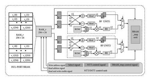
The comparison results between iterative NTT and pipelined NTT implementations are shown in the Table 1. It can be observed that the main advantage of iterative NTT lies in the balance between area overhead and execution clock cycles, making its resource utilization more reasonable and suitable for resource-constrained devices while ensuring performance. On the other hand, pipelined NTT achieves significantly shorter clock cycles at the expense of resource overhead, with the number of cycles for a 256-point NTT transformation being only about one-fifth of that of the iterative approach. While the multiplication unit of MDC-NTT cannot be reused like the iterative NTT, it does not require additional storage units and does not encounter address mapping conflicts, making it more suitable for real-time fast and continuous data transmission. NTT/INTT computations account for a significant portion of the overall protocol’s computational load. Based on the optimized designs for NTT discussed above and considering the practical implementation of the protocol, iterative NTT has an advantage in terms of resource usage but comes with complex process control requirements. Furthermore, when merging NTT/INTT modules in the encryption and decryption steps of the protocol, it increases the complexity of control modules and memory accesses. In contrast, the pipelined structure is better suited for the NTT algorithm within the protocol. When integrated with INTT, it only requires adding postprocessing stages and storage units for each rotation factor level (concatenating NTT transformation rotation factors and inverse transformation rotation factors, taking the high 12 bits during forward transformation and the low 12 bits during inverse transformation). It is essential to note that BR operations must be performed after completing PWM to ensure the accuracy of INTT data. It is important to note that after all multiplication operations here, the data must be restricted to within 3329 through modular reduction. The modular multiplication method for (q = 3329) adopts the algorithm referenced in [21] to perform the operation of obtaining the approximate quotient by division. The specific circuit is shown in Figure 5.
| Type | Slice | LUT | FF | DSP | BRAM | F/MHz | Clock |
|---|---|---|---|---|---|---|---|
| Iterative NTT | 426 | 1264 | 1000 | 2 | 2 | 243 | 1034 |
| Pipelined NTT | 1023 | 3032 | 2632 | 16 | 0 | 272 | 172 |

The characteristics of MDC-NTT, which allows multiple data inputs simultaneously, make it more suitable for high-throughput requirements in large data processing scenarios. However, using two-parallel MDC-NTT units consumes excessive DSP resources without significantly improving hardware efficiency compared to a single MDC-NTT core. When q = 3329, a single MDC-NTT unit consumes only 1749 LUTs and 848 FFs, occupying 501 slices and 8 DSPs. Setting the system period to 3.52 ns meets timing constraints. Therefore, this study implements a single MDC-NTT hardware module for both forward and inverse transformation calculations in the overall circuit of the KYBER-512 protocol’s KEM system.
3.2.1. Other Functional Submodules
Compress, decompress, encode, and decode are important functions in the cryptographic scheme. Its main purpose is to optimize the performance and bandwidth requirements of the protocol during communication. It is also a crucial module in implementing efficient CRYSTALS-KYBER protocol public-key encapsulation circuits.
In the key generation phase of the CRYSTALS-KYBER-512 protocol, the encoding function involved is Encode12. In the encryption phase, the decompression functions involved are Decompressq and Decodel. These functions decode bit 0 as coefficient 0 and bit 1 as coefficient [q/2], respectively.
In the ciphertext “u, ” the compression function compresses the 12-bit coefficients to 10 bits while the Encode10 function reads the decimal sizes of the coefficients from the byte stream. Similarly, in the ciphertext “c, ” the compression function compresses the 12-bit coefficients to 4 bits and the Encode4 function separates the coefficients of individual polynomials.
In the decryption phase, the same parameters are used for the decompression and encoding functions to decompress the ciphertext and obtain the original message. In the decryption phase, the ciphertext “u” and “v” are first restored to 12 bits using the same parameters for the decompression and encoding functions. The Decode12 function is then used to decode the 12-bit polynomial coefficients of the decrypted key. This allows for the next step of polynomial multiplication in the natural number domain.
In these submodules, the decompression function (Decompress) and the decoding function (Decodel) work together, while the compression function (Compress) works with the encoding function (Encodel). Therefore, in hardware implementation, modules that interact with each other are grouped together. The decoding and encoding modules consume minimal hardware resources. Thus, it is important to pay attention to separating and extracting the desired bit widths when performing bitwise operations in hardware.
In the decompression function, dividing by 2d can be achieved by right-shifting (“>> d”) the value, where the shifted-out portion becomes the remainder. In the hardware implementation of the compression function, calculations involving modulo and division by powers of 2 can be achieved using bitwise AND and shift operations. For example, x mod 2d is equivalent to x & (2d − 1).
This provides the value of 2 d/q in the compression function. These modules have low computational complexity and consume a small proportion of resources. It is important to control the data interface signals and optimize parallelism during calculations to reduce the number of clock cycles required.
4. Efficient Public Key Encapsulation Circuit Design of CRYSTALS-KYBER Protocol
4.1. Hardware Circuit Structure
The top-level architecture design of KYBER.CCAKEM for k = 2 in this paper is shown in Figure 6. Existing advanced designs of CRYSTALS-KYBER are mostly based on iterative NTT modules with different numbers of BF units. The control module is commonly implemented using instruction sets or the RISC-V architecture. In this design, MDC-NTT is used to process data in a pipelined manner and the control unit can be implemented using a counter and a state machine to simplify the control module. The signals of the control unit in Figure 6 are shown as thick black lines, and control signal interactions with various functional modules are indicated by flag symbols. In the design, the codec function consumes fewer resources, so it only needs to pay attention to the difference of bit width transformation when reading storage. Due to the inability to reuse the multiplication units in other modules within the pipelined NTT, and based on the Xilinx official documentation [22], FPGA DSP units have a multiplication of 25 × 18 bit, which results in some surplus for the 12 × 12 bit design. Except for the modular multiplication unit designed in MDC-NTT, the multiplication comprehensive realization of 12 × 12 bit small bit width in other calculations is implemented by LUT, which makes resource utilization more reasonable.
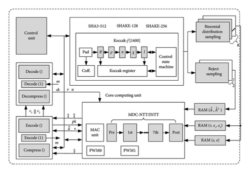
The PRNG module is composed of SHA3-256, SHA3-512, SHAKE-128, and SHAKE-256. It provides random bits to the parallelized binomial distribution sampling and rejection sampling modules. These random bits are temporarily stored in a dual-port BRAM group and then sequentially subjected to NTT transformations for the read polynomial groups. In the key generation phase, four NTT transformations are mainly applied to the s and e terms. The public-key vector computed through matrix-vector polynomial multiplication is completed in the MAC unit of the core calculation module and transmitted to the encryption module in the NTT domain.
After the encryption module completes sampling, the plaintext information m is converted from 0.1 bit to 0 or 1664 by simple Decode (1). In the natural number field, the product of INTT public key and random coins is added. The noise is superimposed to obtain v and 128 bytes of c1 after compression coding. After u being contained, the information of the public-key matrix is compressed and encoded, and a 640 bytes c1 is obtained as well as c2 to obtain the output ciphertext. After receiving the ciphertext, the decryption module first obtains u and v from the ciphertext information through decoding and decompressing. At this time, the key also enters the decryption process from the decoding module. The data containing the plaintext information are obtained after NTT and INTT transformation, and the correct plaintext information is obtained after Encoding (1).
4.2. Hardware Timing Arrangement
The hardware timing arrangement of the key generation module and the hardware timing arrangement of the plaintext encryption and ciphertext decryption modules are shown in Figures 7 and 8, respectively. In the key generation process, there is no INTT involved. The SHAKE-256 function completes four multinomial distribution sampling cycles, including idle clock cycles and hash function iteration clock cycles, totaling 328 cycles. In parallel, SHAKE-128 takes 523 cycles to complete public-key sampling. During the sampling process, the NTT module can be started at the same time. The first polynomial requires 235 cycles to complete the NTT transformation, while subsequent polynomials only need 128 cycles each. Once the NTT transformation is completed, the matrix-vector multiplication is performed immediately. Therefore, the entire key generation process takes only 1458 cycles. Since KEM is basically composed of PKE, the timing relationship of PKE can roughly represent the entire Kyber design, so the timing relationship of the entire KEM is not shown in the timing diagram for simplicity. In the encapsulation process, the SHAKE sampling module and NTT transformation follow a similar pattern. However, since the noise term does not require an NTT transformation during encryption, it is converted into a transposed public-key matrix. The encapsulation process consumes a total of 1792 cycles.
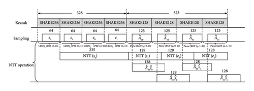
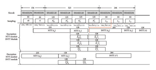
The decode and other functions do not occupy operation cycles and can be calculated in parallel once the main computing unit has completed its tasks. These operations are not shown in the timing diagram.
The decapsulation process includes Encrypt and Decrypt which consumes 2437 cycles. The decoding and decompression operations can be completed when the ciphertext c is loaded. The core calculation part still follows a pipelined structure to avoid unnecessary idle cycles.
5. CRYSTALS-KYBER Overall Implementation Circuit Hardware Design Analysis and Comparison
This section compares and analyzes the above-integrated circuits with the existing advanced designs. When facing different application scenarios, different design methods focus on different optimization directions, so the efficiency of hardware design is an important index to measure the quality of a design. In this section, three calculable indicators, throughput per slice (TPS), operations per second (Op/s), and area time product (ATP) are introduced to evaluate the hardware efficiency of different designs.
5.1. Uniform Weighted Hardware Resources and Efficiency Metrics in FPGAs
In the hardware implementation of cell cryptography, the proportion of on-chip resources used by different design methods is different. Therefore, to make a fair comparison, this section introduces a representative weight conversion method concerning the literature [23] to unify FPGA on-chip resources. The specific resource weights are shown in Table 2. This paper mainly uses the amount of DSP48E and BRAM resources that need to be converted into equivalent Slice areas. LUT and FF will be included in Slice during synthesis, so equivalent conversion is not required.
| Type | Slice | DSP | BRAM | BRAM (36 K) |
|---|---|---|---|---|
| #Slice | 1 | 128 | 166 | 327 |
| Weight | 1.0 | 0.8 | 0.7 | 0.6 |
| ENS | 1 | 102.4 | 166.2 | 196.2 |
Under a uniform equivalent Slice area, TPS, Op/s, and ATP are introduced to fairly compare the performance of different designs. Before giving the calculation method of TPS, first determine the calculation of throughput. The polynomial processed in the MLWE scheme is in vector form, and the plaintext information processed by the system is 256 bits each time. The calculation formula is shown in formula (9).
Op/s indicates the clock cycle that can be executed for encryption and decryption per second. The higher the value, the higher the system performance. TPS weighs throughput and resource consumption. The higher TPS value indicates the higher hardware efficiency. ATP is the product of area and time, which evaluates the area-performance balance, and the lower the ATP value, the more efficient the design.
5.2. Comparative Analysis of CRYSTALS-KYBER Protocol Public Key Encapsulation Circuit Design
Table 3 lists the resource consumption and performance results of the key generation, plaintext encryption, and ciphertext decryption modules of CRYSTALS-KYBER protocol in the Artix-7 platform. A total of 3524 slices are required for key generation. The combined NTT/INTT module has more resources than a single NTT module, consuming a total of 4037 slices. The decapsulation module includes Decrypt and Encrypt and therefore costs more than the encapsulation module, consuming 4184 slices.
| Type | Module | Slice | LUT | FF | DSP | BRAM | F (MHz) | Circles | Latency (μs) |
|---|---|---|---|---|---|---|---|---|---|
| q = 3329 | Key | 3524 | 9626 | 8361 | 8 | 7 | 255 | 1403 | 6.23 |
| CRYSTALS- | Enc | 4037 | 10,762 | 9392 | 10 | 8 | 255 | 1754 | 7.79 |
| KYBER-512 | Dec | 4184 | 11,074 | 10,132 | 10 | 8 | 255 | 2394 | 10.64 |
This paper compares the performance of the CRYSTALS-KYBER protocol’s (KYBER.CCAKEM) public-key encapsulation circuit on the FPGA Artix-7. To ensure a fair comparison, the designs were implemented in Verilog using Xilinx Vivado 2018.3 on the FPGA Artix-7 XC7a35T, with parameters set at 256/3329/2. The resource and performance results for key generation, plaintext encryption, and ciphertext decryption are shown in the last three rows of Table 4.
| Designs | Module | Slice/LUT/FF | DSP | BRAM | F (MHz) | Circles | Delay (μs) | ENS | Op/s | TPS | ATP (10−3) |
|---|---|---|---|---|---|---|---|---|---|---|---|
| Article [21] | KeyGen | 2126/7412/4644 | 2 | 3 | 161 | 3768 | 23.40 | 2679 | 42,728 | 4.08 | 62.71 |
| Enc | 5079 | 31.55 | 31,699 | 3.03 | 84.53 | ||||||
| Dec | 6700 | 41.30 | 24,030 | 2.29 | 111.52 | ||||||
| Article [12] | KeyGen | 3547/10502/9859 | 8 | 13 | 200 | 1882 | 9.41 | 5877 | 106,269 | 4.63 | 55.30 |
| Enc | 2446 | 12.23 | 81,766 | 3.56 | 71.87 | ||||||
| Dec | 3754 | 18.77 | 53,276 | 2.32 | 110.31 | ||||||
| Article [24] | KeyGen | 2200/7300/3200 | 4 | 5 | 200 | 2400 | 12.1 | 3510.6 | 83,333 | 6.01 | 42.48 |
| Enc | 3000 | 15.0 | 66,667 | 4.86 | 52.66 | ||||||
| Dec | 4200 | 21.2 | 47,619 | 3.47 | 73.72 | ||||||
| Article [25] | KeyGen | 2040/6910/3270 | 3 | 3 | 200 | 2960 | 14.3 | 2828 | 67,567 | 6.12 | 41.85 |
| Enc | 3910 | 21.8 | 51,150 | 4.63 | 55.28 | ||||||
| Dec | 5230 | 30.4 | 38,240 | 3.46 | 73.95 | ||||||
| Article [15] | KeyGen | 5273/13999/12503 | 2 | 0 | 208 | 1100 | 5.3 | 5473 | 189,090 | 8.64 | 28.94 |
| Enc | 1500 | 7.2 | 138,666.7 | 6.49 | 39.46 | ||||||
| Dec | 2100 | 10.1 | 99,047 | 4.63 | 55.25 | ||||||
| This design | KeyGen | 3524/9626/8631 | 8 | 7 | 225 | 1403 | 6.23 | 5136 | 160,371 | 7.99 | 32.03 |
| Enc | 4037/10762/9392 | 10 | 8 | 1754 | 7.79 | 5965 | 128,278 | 5.51 | 46.50 | ||
| Dec | 4184/11074/10132 | 10 | 8 | 2394 | 10.64 | 6112 | 93,985 | 3.94 | 65.03 | ||
- Note: The bold values in the table are used for comparison in the text, indicating metrics that outperform other designs.
The major advantage of the pipelined NTT-based CRYSTALS-KYBER protocol’s public-key encapsulation circuit in this design is its low latency. The total time to complete the KEM is only 24.66 us, with the three modules consuming 3524, 4037, and 4184 slices, respectively.
In the other works, [21, 24, 25] are similar compact designs for Kyber. Their NTT architecture requires less DSPS due to the use of iterative NTT, which results in a lower overall resource overhead than this design. However, our design reduces execution time by 38.9% compared to [24] and improves the number of Op/s by 51%–76% taking full advantage of MDC-NTT. In the design [25] for the optimization of running time and data throughput, this design also has the advantages of running time and Op/s. Compared to reference [15], the NTT structures used are different, resulting in a significant difference in the number of DSPs, with our design being more suitable for high-performance applications. While this paper is still comparable to [15] in terms of overall time consumption and resource overhead, our design is more flexible in practical applications due to the separation of the three functions.
Based on the above analysis, the MDC-NTT-based CRYSTALS-KYBER protocol’s public-key encapsulation circuit offers high throughput and low latency with a slight increase in resources. To reduce the number of DSPs used, the multiplication in the MDC-NTT structure is implemented using DSP48E1, while other parts utilize LUT synthesis, making the resource allocation more reasonable. This design has practical application value in scenarios such as vehicles, aircraft, and any situation requiring fast and continuous communication.
6. Conclusion
This paper presents an efficient hardware implementation of the CRYSTALS-KYBER lattice-based public-key encapsulation scheme based on the MLWE protocol. The paper focuses on optimizing the hash sampling module and polynomial NTT operation module in the CRYSTALS-KYBER protocol. The designed hardware circuit has a KEM execution period of only 24.66 us, achieving efficient encryption and decryption performance. Furthermore, the resource consumption and performance of KYBER.CPAPKE hardware circuits are compared with other lattice-based circuits using three computable parameter indicators: TPS, Op/s, and ATP. The CRYSTALS-KYBER public-key encapsulation circuit KYBER.CCAKEM requires only 5551 clock cycles to execute. The maximum operating frequency also reaches up to 225 MHz, making it more suitable for real-time data transmission. In the future, we will further complete the complete KEM protocol circuit of CRYSTALS-KYBER protocol on the basis of this study and explore more optimization directions.
Conflicts of Interest
The authors declare no conflicts of interest.
Author Contributions
The authors Song Cheng and Jiansheng Chen contributed equally to this work.
Funding
This work was supported by Beijing Smartchip Microelectronics Technology Co. Ltd., Laboratory Open Fund Project with Grant No. SGSC0000SJQT2207160.
Open Research
Data Availability Statement
Data supporting the findings of this study are available from the corresponding author upon reasonable request.


