Pressure-Induced Physical and Optoelectronic Properties of Noble Cs2HfInBr6 for Enhanced Solar Energy Harvesting
Abstract
Exploring advanced materials for energy device applications is paramount for efficient and sustainable energy solutions. Here, density functional theory (DFT)-based simulations are carried out to systematically investigate the physical properties of a noble hafnium (Hf)–indium (In)-based Cs2HfInBr6 halide double perovskite (HDP). We demonstrate that pressure-induced lattice confinement leads to significant changes in structural and electronic properties, resulting in transitions from semiconductor to metallic phases simultaneously direct to indirect band gap transition. Tunable electronic properties of the proposed Cs2HfInBr6 perovskite portray advantageous light–matter interaction behavior, which suits this material for advanced optoelectronic devices and biomedical applications. DFT-simulated physical behavior modeled with the finite difference time domain (FDTD) theoretical device modeling the Cs2HfInBr6 solar cell demonstrates excellent power conversion efficiency of up to 27.5% with a single crystal in the planar cell under 7 GPa external pressure. This study advances energy and device engineering research by setting Cs2HfInBr6 double perovskite as a promising contender for future renewable energy technology. Moreover, its unique electronic properties of multiferroic Hf─In combinations in perovskites research would pave the exciting opportunities for advancing the next generation of electronics.
1. Introduction
Halide perovskite semiconductors are known for their electronic properties including tunable bandgap, high carrier mobility and defect tolerance, and high absorption coefficient [1]. With the chemical formula ABX3, the perovskite compounds show phenomenal efficiencies in converting power, which can complement or even surpass the traditional Si-based solar cells [2]. Their crystal structure is formed with corner-sharing of octahedral B cations coordinating to X halogens, whereas the tetrahedral sites are occupied by A cations. A little change in chemical composition of halide perovskites, everyone is after achieving the desired bandgap from 1.5 to 3.0 eV bandgaps [3] for optoelectronic behavior of the newly formed material.
Over the past decade, inorganic perovskites have predominantly led to the field of perovskite photovoltaics compared to organic and organic–inorganic hybrid counterparts, attributed to their enhanced thermal stability [4]. Furthermore, inorganic halide perovskites have gained significant attention due to their superior absorption coefficients, resilience to defects, controlled tunability in band gap and carrier dynamics, longer diffusion lengths, ultralow thermal conductivity, reduced exciton binding energy leading to prolonged carrier lifetimes, and higher mobility of charge carrier and cost-effectiveness, among other favorable attributes [5–8].
Leveraging nanotechnology, perovskite applications extend to nonlinear optics in nanophotonic structures that confine light and increase interaction. This exploits the sub-bandgap advancements in metal halide perovskites due to multiphoton absorption, which can lead to the next generation of nonlinear photonic devices [9]. This amplifies the efficacy of perovskite-based solar cell devices. Perovskite crystals exploit spin–orbit coupling and lattice symmetry for low-power spintronics, and lattice engineering within the crystal framework advances potential in quantum computing by controlling spin-polarized electron density without external magnetic fields [10, 11]. This symmetry engineering can enhance spin photocurrent generation for next-generation perovskite-based spin optoelectronic devices [12]. The tunable physical properties of perovskites have significantly boosted perovskite solar cell (PSC) efficiency, soaring from 3.8% (2009) to over 25% (2023) with single crystal halide perovskites [13, 14].
Inorganic halide double perovskites (HDPs) (A2BB′X6), a transformative subclass of ABX3 perovskites, are emerging as promising solutions, showcasing advancements and correlated electron properties for diverse electronic applications beyond photovoltaics [15, 16]. Understanding and proficiently manipulating the optoelectronic properties of perovskites encompass diverse strategies such as chemical composition modification, doping, strain engineering, phase control, temperature and dimensional tuning, and others [17–21].
Noble perovskite discovery by approaching chemical compositional variations is a simpler and more effective method for material design for a desired application. For an example, modifying the chemical composition in perovskite crystals, like altering from bismuth (Bi) to indium (In) at B-site in the double Cs2InAgCl6 perovskite and substituting different X-site atoms in Cs2LiInX6, induces varied atomic radius led octahedral tilt within the inorganic framework that results in a customizable indirect–direct band gap transitions and proves effective in enhancing optical properties making them suitable for solid-state photoelectronic devices [20, 22]. Moreover, the variation in A-site cations within A2LiInBr6 perovskites demonstrates efficient UV-to-visible optical absorption with notable thermal efficiency for solar energy conversion in solar cells [23]. Utilizing the electronegativity of halogen atoms, double perovskites with mixed halide compositions—Cs2AgBiBr6-xClx—demonstrate effective controllability in the band gap of materials, thereby modifying the effective masses and optical absorption of perovskites for tailored applications in advanced photoelectronics [24].
Now, external pressure can significantly tune the electronic properties of materials such as reducing the bandgap, shifting the absorption peak to low photon energy [25, 26], which may, in turn, increase the suitability of the material to be used in optoelectronic applications. Such double-phase perovskites can be effectively tuned through applied pressure, where a synthesis pressure of 7 GPa has been shown to modify their structural, electronic, and optoelectronic properties—enhancing their potential for solar cell applications. While achieving such pressures experimentally for operational solar is challenging, techniques like diamond anvil cells and substrate-induced strain offer practical avenues for replicating these effects in lab-based studies [27]. Moreover, in the tandem-type solar cell, one may need to use a perovskite absorber layer under pressure due to the lattice mismatch with the lower or upper absorber layer [27].
The study of Cs2HfInBr6 is motivated by its unexplored compositional space and the promising properties of its constituent elements: Hf and In. Hf is known for its high dielectric constant, stability, and strong spin–orbit coupling, which are advantageous for optoelectronic applications and can enhance the material’s thermal and ambient stability [28, 29]. On the other hand, In has been shown to improve optical absorption and modify electronic properties in perovskites, which can be beneficial for tuning the bandgap and enhancing other optoelectronic characteristics [30, 31]. Combining these two elements at the B-site in DHPs presents a unique opportunity to discover new material properties that could lead to significant advancements in optoelectronic devices. A very recent study explores Hf-based HDPs Cs2HfX6, which highlights that, due to the vacancy ordering effect in the crystal structure, the Hf-based compound exhibits increased octahedral tilting, resulting in a shift from an indirect to a direct energy band gap [32]. Besides, Cs2HfCl6-based PSCs, synthesized for ambient conditions, exhibit wide bandgap properties, luminescence with significant Stokes shifts, and emission from self-trapped excitons, indicating promise for scintillation and other optical applications [33].
However, experimentally, Cs2HfCl6 double perovskite nanocrystals are defect-intolerant semiconductors, and this issue can be addressed through Sb doping to prevent the formation of sub-bandgap defect states [34]. Also, Hf-based perovskites show exceptional photocatalytic activity under visible light, whereas with paramagnetic transition metal cation Hf, Hf-based perovskites offer higher dielectric behavior suitable for storage capacitor applications [35, 36].
Despite various studies on double perovskites with distinct chemical compositions involving In and Hf individually, there is a gap in the literature regarding their combined use in the B-site of DHPs. This study addresses this gap by exploring the physical properties of Cs2HfInBr6 under different pressures, investigating its photovoltaic device behavior through multimodal density functional theory (DFT) and finite difference time domain (FDTD) methods. This theoretical study can provide useful insight to the experimentalist to synthesize Cs2HfInBr6 double perovskite for optoelectronic applications.
2. Crystal Structure and Methodology
The Cs2HfInBr6 HDP crystal structure was modeled using VESTA [37]. The cubic halide perovskite’s ABX3 unit cell was obtained from the Materials Project and transformed into a 2 × 2 × 2 supercell to form the A2BB′X6 double perovskite unit cell. In this configuration, the A-site is occupied by Cs (Z = 55) atoms, the X-site is filled with bromine (Br) atoms, and the B-site has a 50% distribution of Hf and In atoms, resulting in a crystal with 40 atoms in the unit cell. The crystal unit cell underwent geometry optimization and extraction of physical properties using first-principal calculations. Utilizing the extracted optoelectronic data, the perovskites were incorporated into a device structure to evaluate their practical light–matter interactions of the built Cs2HfInBr6 perovskites in the devices.
2.1. Computational First-Principle Approach
The conventional unit cell structures of Cs2HfInBr6 (each comprises 40 atoms), as shown in Figure 1a, were fully optimized to ground state energy through DFT implementations. This study delves into the detailed analysis of perovskite crystal structure, electronic band dispersions and state density, elastic modulus, and optical properties using the plane wave pseudopotentials method, specifically implemented through the Cambridge Serial Total Energy Package (CASTEP) in Materials Studio [38]. The evaluation of exchange–correlation interactions within Kohn–Sham orbitals during geometry optimization and subsequent electronic energy calculations was performed using the Perdew–Burke–Ernzerhof (PBE) function within the generalized gradient approximation (GGA) [39, 40].
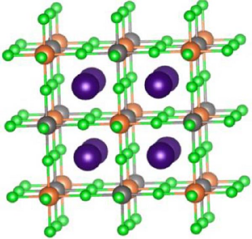
A wavefunction energy cutoff of 500 eV for prolonging plane waves and an 8 × 8 × 8 Monkhorst–Pack k-point mesh centered at Γ were utilized to sample the first Brillouin zone (BZ) of the Cs2HfInBr6 double perovskite crystal [41]. Lattice constant, cell volume, and atom positions were optimized without any symmetry constraints until the residual force per atom is <0.006 eV/Å. The self-consistent electronic relaxation was carried out with convergence energy and force criteria set at 10−6 eV and 0.02 eV/Å, respectively, and the calculations considered spin polarizations. In this study of the Cs2HfInBr6 double perovskite, the electronic configurations of valence states are Cs+1:5p66s1, Hf+4:4f145d26s2, In+3:4d105s25p1, and Br−1:3d104s24p5. Each Hf and In atom is coordinated with six Br atoms, forming alternating (HfBr6)2− and (InBr6)3− octahedra, while Cs atoms occupy the voids within the lattice to maintain charge neutrality. Vanderbilt [42] ultrasoft pseudopotential in the CASTEP code was utilized for the atomic potentials. To understand the pressure influence on the optoelectronic and mechanical attributes of Cs2HfInBr6, double perovskite is studied within the range spanning from 0 GPa to 25 GPa.
2.2. Device Architecture Modeling and Simulation
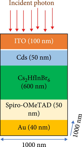
First-principle calculations optimized the nonleaded noble Cs2HfInBr6 material could utilized as the light photon-absorbing material in a photovoltaic device featuring an n-i-p configuration. The schematic representation of the multilayer PSC structure is depicted in Figure 1c. The modeled device utilizes Spiro-OMeTAD as the electron transport layer (ETL) and cadmium sulfide (CdS) as the hole transport layer (HTL). It consists of In-doped tin oxide (ITO) on a transparent glass substrate as the top layer, serving as the cathode, with gold (Au) acting as the back metal anode contact. ITO, chosen for its optical transparency, substrate adhesion, and chemical inertness, is utilized as the cathode layer, while Au, selected for its enhanced electrical conductivity, stability, and compatibility with perovskite materials, serves as the back metal contact. The layer thicknesses in the structure (ITO, CdS, Cs2HfInBr6, Spiro-OMeTAD, and Au contact) are 100, 50, 600, 50, and 40 nm, respectively. For the necessary equations used in the computational calculations, please see the Supporting Information.
3. Properties of Cs2HfInBr6
3.1. Structural Phase Stability
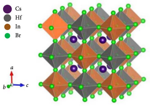
The CASTEP performed geometry-optimized double perovskite Cs2HfInBr6 which crystallizes in the cubic phase of the Fmm (no. 225) space group at room temperature, as represented in Figure 1b. The double perovskite crystal consists of 8 Cs atoms at the Wyckoff position 8c of the cell with coordinates (1/4 1/4 1/4), 13 Hf atoms are at the Wyckoff site 4b at (1/2 1/2 1/2) coordinates, and 14 In atoms are at Wyckoff site 4a positioned at (0 0 0), while 5 halide Br atoms occupy the Wyckoff site 24e with (x, 0, 0) positions. Within the crystal, B-site’s 13 (Hf–Br6) and 14 (In–Br6) atomic compositions construct an inorganic octahedral framework, as shown by the polyhedral formation in Figure 1b. Utilizing the ionic Shannon radii of individual atoms in the Cs2HfInBr6 compounds yields a tolerance factor of 0.89, aligning with the stable range of 0.81 < t < 1.1, thus confirming their stability in accordance with the Goldschmidt rule following equation (Supporting Information Equation (2)). Analyzing crystal stability under different physical conditions (i.e., pressure and volume), we employed Birch–Murnaghan equation (Supporting Information Equation (1)) of states to optimize energy/pressure–volume behavior, investigating optimal lattice constants for Cs2HfInBr6 double perovskites. The ground state structure was determined by minimizing the crystal energy with respect to the volume, as shown in the E–V fitting plot in Figure 2a, confirming the structural stability of these perovskites.

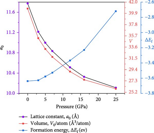
The Cs2HfInBr6 perovskites exhibit a consistent decrease in equilibrium lattice constants from 7.97 to 6.96 Å as hydrostatic pressure varies from 0 to 25 GPa, as exhibited in Figure 2b and listed in Table 1. This trend results from structural atomic position modifications under pressure, aiming to minimize energy and resulting in decreased interatomic distances. Volumes under pressure variations are consistent with lattice parameters, as shown in Figure 2b. The formation energy (ΔEf) is a crucial indicator of thermodynamic stability in DHPs, reflecting the energy balance during defect creation and compound formation. Lower formation energies suggest enhanced stability and favorable synthesis conditions. Calculated formation energies with equation (Supporting Information Equation (4)) are detailed in Table 1, and trends under varying pressure are depicted in Figure 2b, with negative values indicating thermodynamic stability and exothermic behavior for the noble compound. However, with increasing pressure, this parameter value goes up from −3.64 to −2.72 eV/atom in the negative magnitude.
| Parameters | Cs2HfInBr6 | ||||||||
|---|---|---|---|---|---|---|---|---|---|
| 0 GPa | 3 GPa | 5 GPa | 7 GPa | 12 GPa | 16 GPa | 25 GPa | |||
| Structural | a0 (Å) | 11.7710 | 11.2143 | 10.9997 | 10.8324 | 10.5130 | 10.3243 | 10.1075 | |
| V0/atom (Å3/atom) | 40.7739375 | 35.258055 | 33.272817 | 31.77768 | 29.0485 | 27.51207 | 25.8155125 | ||
| E0 (eV/atom) | −3.753518 | −3.752930 | −3.752681 | −3.752334 | −3.751501 | −3.750893 | −3.750015 | ||
| Formation energy, ΔEf | −3.6391 | −3.6301 | −3.5826 | −3.5287 | −3.3673 | −3.2324 | −2.7245 | ||
| T | 0.89 | ||||||||
| Electronic | Eg | 2.08 | 1.99 | 1.99 | 1.33 | 0.729 | 0.287 | 0 | |
| Effective mass | me ∗ | 0.257 | 0.393 | 0.425 | 0.451 | 0.488 | 0.495 | 0.331 | |
| mh ∗ | 0.181 | 0.149 | 0.143 | 0.131 | 0.127 | 0.127 | 0.096 | ||
Since the stability of the double perovskites is important for the suitability of fabrication and commercialization, we also need to check the thermodynamic stability of Cs2HfInBr6 materials, which can be demonstrated by obtaining their decomposition enthalpies (ΔH). The basic and most convenient decomposition method for our considered double perovskite is breaking them into their corresponding binary compounds. We calculate the ΔH of Cs2HfInBr6 utilizing the GGA–PBE exchange functional from the total energies with respect to three suitable decomposition pathways. The difference between the total energy of the considered material and the total energy of the disintegrated binary compounds is used to determine the decomposition enthalpy of Cs2HfInBr6 double perovskite.
- 1.
Cs2HfInBr6 = 2CsBr + HfBr3 + InBr; ΔHd = −17.2 (meV/atom).
- 2.
2Cs2HfInBr6 = Cs3Hf2Br9 + CsBr + 2InBr; ΔHd = −5.4 (meV/atom).
- 3.
; ΔHd = −358.4 (meV/atom).
The minimized total energy was obtained for each compound after full relaxation was secured. A positive value of ΔH indicates the spontaneous nature and instability of the materials, while a negative enthalpy confirms the thermodynamic stability of the compounds. We have taken binary crystal systems of CsBr cubic (), Cs3Hf2Br9 trigonal (), InBr3, and HfBr3 monoclinic (c2/m), Cs3Hf2Br5 hexagonal (P63/mmc), and InBr with cubic (), respectively. On these pathways, this crystal showed thermodynamically stable. As far as literature goes, there is no accessible experimental data for the structural behavior of the double Cs2HfInBr6 halide perovskites. Nevertheless, our computed structural data and behaviors align with prior experimental and theoretical studies on other analogous compounds [46].
3.2. Dynamic Stability
Phonon dispersion describes how vibrational energy (frequency) varies with momentum (wave vector) in a crystal lattice. Figure 3 presents the calculated phonon dispersion for the Cs2HfInBr6 compound, obtained using the CASTEP code and DFPT [38]. The plot includes the longitudinal optical/transverse optical (LO/TO) splitting effect caused by the electric field, analyzed along high-symmetry paths in the BZ under hydrostatic pressures of 0, 3, and 7 GPa. The phonon spectrum consists of 30 branches arising from the 10 constituent atoms, comprising three acoustic modes and 27 optical modes. Importantly, the absence of imaginary frequencies in the phonon spectra at all pressures confirms the compound’s kinetic stability. These results suggest that Cs2HfInBr6 is dynamically stable under different hydrostatic pressure range investigated, with no structural instabilities detected.

3.3. Bader Charge Analysis
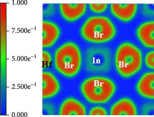
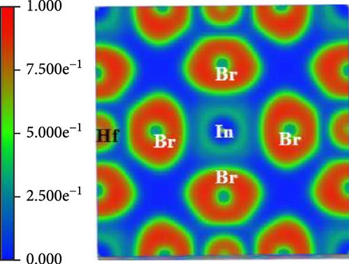
The Bader charge analysis reveals pressure-dependent electronic and bonding changes in Cs2HfInBr6. At 0 GPa, the Bader charges for In, Hf, Cs, and Br are 0.66581, 1.791, 0.87561, and −0.701441, reflecting ionic bonding with balanced charge distribution, as tabulated in Table 2. Also in Figure 4a, the electron localization function (ELF) map at 0 GPa pressure shows localized electron density around Br atoms and moderate delocalization around Cs and In atoms, indicating ionic In─Br and Cs─Br interactions [47].
| Elements | Bader charge (0 GPa) | Bader charge (3 GPa) | Bader charge (7 GPa) |
|---|---|---|---|
| In | 0.66581 | 0.704276 | 0.660269 |
| Hf | 1.791 | 1.884825 | 1.00061 |
| Cs | 0.87561 | 1.281884 | 0.791424 |
| Br | −0.701441 | −0.71759 | −0.54423 |
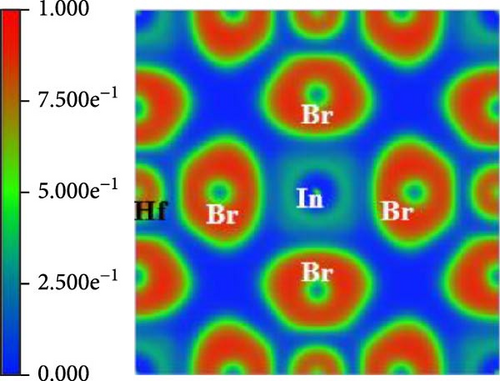
At 3 GPa pressure-enhanced Coulomb interactions increase electron localization around Hf and Cs (charges rise to 1.884825 and 1.281884), while Br becomes more electronegative (−0.71759), indicating stronger ionicity [48]. For validation, the ELF maps (Figure 4 b) show sharper electron localization around Br and more pronounced bonding regions between Br and Cs/In, suggesting stronger ionic In─Br and Cs─Br bonds under pressure. Furthermore, at 7 GPa, lattice compression and orbital hybridization reduce Hf and Cs localization (charges drop to 1.00061 and 0.791424), and Br’s charge becomes less negative (−0.54423), signifying a shift toward covalent Hf─Br bonding [47, 48]. The localization map at this pressure shows enhanced delocalization in Hf─Br bonds presented in Figure 4c, with reduced localization around Cs and In, indicating pressure-induced covalency in Hf─Br and weaker ionic interactions for Cs─Br and In─Br bonds. This highlights the potential of pressure as a tool to fine-tune the electronic and structural properties of Cs2HfInBr6, opening avenues for advanced applications in optoelectronics, high-pressure sensing, and energy materials.
3.4. Electronic Properties
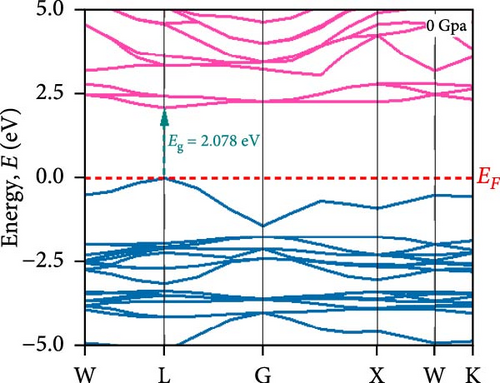
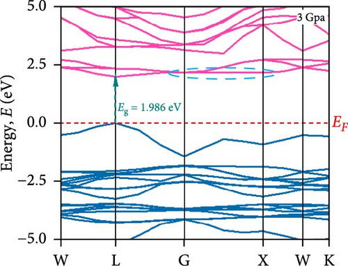
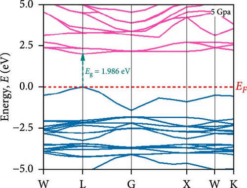
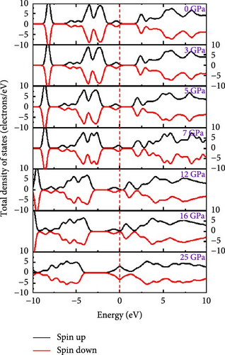
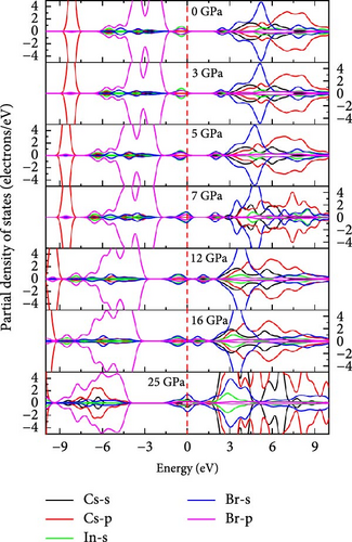
To understand the energy distribution nature of electrons in the noble Cs2HfInBr6 double perovskite along with different applied pressure effects on its electronic states and consequently optical behavior, energy band profile (E–K dispersions) and electron DOS are evaluated within GGA–PBE functional. The E–K dispersions are represented in Figure 5a–g for the HfIn-based double perovskite under different pressure conditions. Figure 5 illustrates the electronic energy band structures along high-symmetry paths in the first BZ. The band edge dispersions in Cs2HfInBr6 exhibit a consistent trend that the conduction band minima (CBM) and valence band maxima (VBM) remain at the same K-path within the BZ. This alignment persists up to the applied pressure of 16 GPa from ambient conditions, corroborating the semiconducting nature of the material with direct band gaps. Usually, following Shockley–Queisser efficiency, a suitable absorber material for efficient photoelectric conversion should have a bandgap within 0.9–2.2 eV [49]. At ambient pressure (0 GPa), Cs2HfInBr6 exhibits a semiconducting nature with a band gap of 2.08 eV. However, applying pressures ranging from 1 to16 GPa leads to a reduced electronic band gap from 1.97 to 0.29 eV, indicative of a potential semiconducting to conduct transition behavior. The band edge dispersions of the conduction and valence band exhibit a similar trend under pressure variations from 0 to 16 GPa, as depicted in Figure 5a–f. The conduction band structure undergoes downward shifts toward the Fermi level with increasing pressure, while increased pressure leads to shifts down in valence band states other than the VBM toward deeper energy levels. It is worth noting that there is an inverse relationship between band gap and external pressure [50], as well as the repulsion of the maximum valence band and other valance bands [51, 52] which leads to an increase in the potential between electrons and ions, responsible for reducing lattice parameters (Table 1). Orbitals from Br-p and In-s atoms can hybridize, forming bonding and antibonding states. The highest valence band is often an antibonding state, which naturally lies higher in energy than bonding states [53]. Also, in Cs2HfInBr6 with lower symmetry and applied pressure, the crystal field as well the lattice can cause the splitting of degenerate states, raising one state higher in energy [54, 55]. Furthermore, at 25 GPa, there is observable overlap between both the CBM and VBM along different high symmetry k-paths; specifically, the VBM shifts to the left between the W → L k-points, while the CBM shifts to the G point from L. This implies a direct-to-indirect transition in the conduction mechanism alongside a semiconductor-to-metallic phase shift in the studied double HfIn halide perovskite under pressure [56]. Moreover, the presence of flat bands within the conduction band (circled in Figure 5b) hints a potential secondary phase may contribute to the onset of superconductivity [57]. Intriguingly, as pressure increases, the flat bands near the Fermi level realize the transition to a dispersive nature, as illustrated in Figure 5f,g.
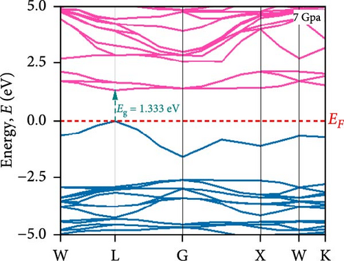
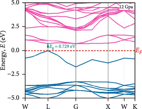
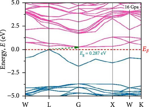
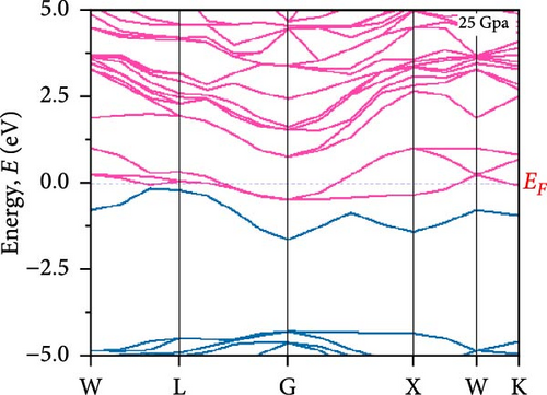
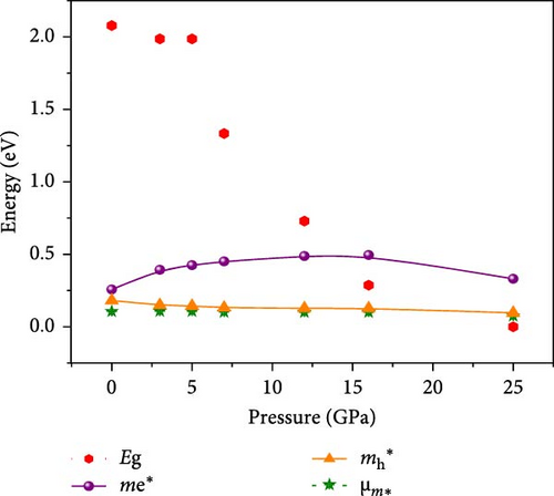
Pressure-induced changes in effective mass enable tailored electronic behavior of the Cs2HfInBr6 perovskite to improve device performance in photovoltaics, transistors, sensors, and advanced nanoelectronics [58]. In semiconductor physics, effective mass, inversely related to CBM and VBM bandwidth, is determined by the curvature of the energy dispersion relation near band edges [59]. A reduced bandwidth implies a more localized wavefunction, resulting in a higher effective mass for charge carriers. The conduction band edge shows superior dispersion with a larger bandwidth compared to the valence band. Influenced by Cs s states for the bottom conduction band and p and d states of B-site cations for the top valence band, bandwidth narrowing occurs due to reduced localization. Effective masses (m∗) for electrons and holes are determined using band-edge eigenvalues and wave vectors near the VBM and CBM through equations (Supporting Information Equations (5) and (6)) and detailed in Table 1. Figure 2c illustrates the correlation between band structures and effective masses, showcasing the impact of pressure on electronic charge-carrier dynamics and band gaps in Cs2HfInBr6 double perovskite. In the L k-space, the effective mass of electrons (m∗) increases from 0.257 at 0 GPa to 0.495 at 16 GPa with increasing pressure. This behavior arises from the compression of the lattice under applied pressure, which reduces interatomic bond lengths and induces octahedral tilts. These structural changes modify the band edge profiles of the perovskites, as shown in Figure 5, and affect the movement of charge carriers by altering the electronic band structure [58, 60]. Consequently, the deformation of the crystal lattice and resulting changes in electronic band profiles influence the optical properties, suggesting pressure-induced band modulation effect under applied pressure [61]. However, at 25 GPa, the band gap becomes 0 eV, the material becomes metallic in nature, and electrons can move freely in the whole crystal lattice, which reduces its effective mass. As pressure compresses the crystal lattice, increased electronic localization within the crystal lattice results in higher effective mass for electrons, reducing electron mobility due to constrained movement in the tighter lattice. Though electron mobility reduces the effect of applied pressure for the Cs2HfInBr6 perovskite, me ∗ values are still smaller than the standard MAPbI3 (30% PCE) [62]. Therefore, deliberate reduction of electron mobility can enhance characteristics in switching, stability, or sensing applications, while the usual goal is to maximize mobility for better device performance and efficiency. Besides, Table 1 and Figure 1c show that under 0–25 GPa pressure, hole effective mass (mh ∗) consistently decreases from 0.181 to 0.096. This suggests higher hole mobility within the crystal lattice, facilitating faster charge transport and more effective charge extraction with an applied electric field. Semiconductors with lower hole effective mass would improve electrical conductivity and enhance charge carrier dynamics, making them suitable for applications like transistors, solar cells, and photodetectors, where efficient charge transport is crucial for energy conversion [63].
To understand the atomic orbital contribution to optoelectronic behavior of the Cs2HfInBr6 perovskite by influencing both CBM and VBM, the GGA–PBE function employed the total density of states (TDOS) and partial density of states (PDOS) which are evaluated and represented in Figure 5h,i from −10 to 10 eV energy range. Aligning with the band structure, the TDOS plot in Figure 5h, the top of the valence band (VBM) is predominantly localized with In and Br atoms, encompassing the Fermi level from −6 to 0 eV. The TDOS peaks attributed to B-site atoms are situated around 2.5 eV in the conduction band and −5 eV in the valence band. With increasing pressure, the TDOS plot indicates a shift of the conduction band edge toward the Fermi level more than the VBM, resulting in the band merging of both CBM and VBM at 25 GPa, where Br atom dominates the Fermi level. PDOS refines TDOS by identifying atomic orbitals contributing to electronic behavior, providing insights into energy-dependent properties and photon–matter interaction control at the quantum level. It also reveals bonding characteristics and hybridization effects on material properties by identifying orbitals influencing valence and conduction bands. In-5s and Br-4p orbitals dominate in shaping the valence band edges to the fermi level, with a slight contribution from Br-4s. In contrast, the conduction band is ~2.5 eV above the ground state and experiences hybridization induced by external pressure among In-5s, Br-4p, and Br-4s orbitals, lowering the CBM at the L point to the fermi energy as evident from PDOS plots in Figure 5i. As pressure increases, the dominance in the valence band near the fermi level shifts from In-5s to Br-4s (at 5 GPa), while in the conduction band, Cs-4s and 4p states increase, and Br-s orbital contributions decrease. At 25 GPa, band merging by Cs-s, Br-s orbitals’ hybridization at Fermi level results in a transition from semiconducting to metallic phase as also depicted in band structure (Figure 5g), where the dominance of Br-4s orbital is evident. The pressure-induced electronic energy analysis indicates band edge shifts attributing to the effect of defect energies by Hf and In ions, aligning with experimental observations for persistent structural deformation and desired band gap transformation in perovskite compounds [25]. The observed controllable band gap shifts and phase transitions in Cs2HfInBr6 sets it as a promising perovskite for advanced applications in spin-optoelectronics, transistors, etc., leveraging tailored carrier dynamics for improved performance and versatility beyond efficient photovoltaic devices.
3.5. Photon–Matter Interactions of Cs2HfInBr6 Perovskite
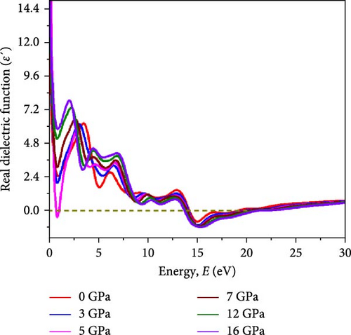
Optical analysis of Cs2HfInBr6 perovskites reveals the intricate interaction between photons and electronic structures, influencing photon absorption, electron excitation, and emission crucial for solar cells and optoelectronic devices. Understanding quantum-level light–matter interactions is paramount for optimizing halide perovskite device performance, aligning with electronic properties that facilitate tailored applications in transistors, detectors, lasers, sensors, and photonics. Implementing with GGA–PBE, optical properties of the Cs2HfInBr6 perovskite under different pressure conditions are evaluated, including dielectric functions, photon absorption spectra, refractive index and extinction, reflectivity, and corresponding optical loss in the energy range of 0–30 eV and illustrated in Figure 6. Modifications in lattice structure, band gap, and electronic properties induced by pressure can directly affect the dielectric function [64]. Transitions of electrons between valence and conduction bands induce alterations in dielectric behavior, influencing charge carrier polarization and mobility within the crystal lattice in response to an electric field, affecting the material’s energy storage and transmission efficiency [63]. Moreover, dielectric properties govern the interaction between incident light and collective electron oscillations (plasmons), shaping the plasmonic behavior of plasmons propagating, resonating, and interacting with incident light, subject to applications in light manipulation, sensing, and energy harvesting [65]. Comprised of the real part (ε1(ω)) and the imaginary part (ε2(ω)), the dielectric function is expressed as ε(ω) = ε1(ω) + iε2(ω). By utilizing momentum matrix components between occupied and unoccupied wave functions, equation (Supporting Information Equation (7)) from the Kohn–Sham equation was utilized to derive the imaginary dielectric constant (IDC), ε2(ω). The ε2(ω) shapes the optical absorption bandwidth in semiconducting perovskites, with peaks indicating resonant frequencies tied to excitonic effects and electron–hole pair (EHP) creation during interband electronic transitions [66].
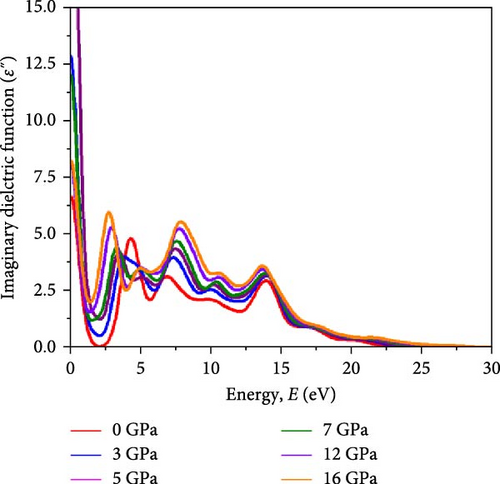
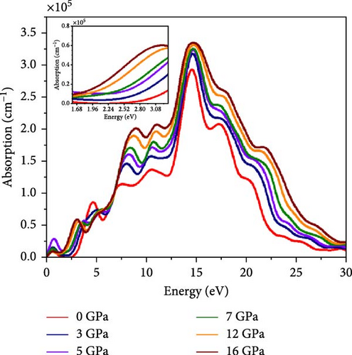
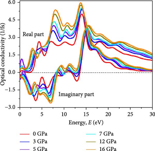
Variations in ε2(ω) dispersions with applied pressure for the HfIn based HDPs are represented in Figure 6b. The first peak in ε2(ω) signifies absorption energy associated with transitions from valence to conduction bands. As illustrated in Figure 4b, the compound in all pressure conditions shows a subdued magnitude of IDC at E = 0 eV, suggesting negligible energy dissipation within crystal systems at zero photon energy. The initial sharp peak of IDC for the Cs2HfInBr6 perovskite at 0 GPa occurs at E = 4.3 eV, as depicted in Figure 6b, and shifts to E = 2.5 eV with increasing pressure. The dielectric function’s peak at 4.3 eV signifies strong absorption of vacuum UV light by the perovskite, which shifts to the visible spectrum under pressure, as evident in Figure 6c. The UV peak implies excitonic effects, influencing EHP creation and movement to regulate charge carrier dynamics [32]. At 0 GPa, the material may seem transparent to visible light, transitioning to a solar radiation absorber under increased pressure [24]. This tunability can be advantageous for these materials for designing advanced opto-spin-electronic applications.
In Figure 6a, the real part of the dielectric constant (RDC) ε1 (ω) spectra for Cs2HfInBr6 under pressures ranging from 0 to 16 GPa, calculated using the Kramers–Kronig transform following equation (Supporting Information Equation (8)), demonstrates the material’s polarization response to an external electric field across the same energy range as ε2(ω). The dipole momentum transfer matrix between and in ε1(ω) influence polarization behavior of the material in effect of external electric field induced charge displacement within crystal lattice directly govern the dispersion behavior. Thus, quantifying susceptibility with ε1 (ω) is vital for understanding the material’s energy storage ability and dielectric response to electromagnetic waves portraying polarization behavior and charge displacement in the crystal lattice under an applied electric field by P(ω) = χ(ω)ε0E(ω) = [ε1(ω) − 1]ε0E(ω). The oscillating electric field in a linear optical field induces polarization with frequency ω universally, using low to medium light intensities of electromagnetic waves. The real component of the dielectric constant ε1(ω) underwent a significant rise at 0 eV until reaching its peak value, followed by a decline toward unity after an inflection point around 16 eV. The increase in pressure results in an increasing trend in real dielectric behavior, as depicted in Figure 6a. The peak magnitude in ε1(ω) shifts from UV to visible range under pressure, with ε1(ω) trends paralleling ε2(ω) except at 5 GPa, where ε1(ω) decreases from 0 GPa. Besides, higher values of ε1 lead to higher refractive indices, which is comparable with Figure 7a, which shapes the light propagation behavior in the material. Higher dielectric constants in materials correspond to reduced charge–carrier recombination rates, thereby improving optoelectronic device performance, particularly influencing charge transport in devices such as transistors [30]. Figure 6a,b illustrates that increasing pressure leads to higher magnitudes in both the real and imaginary parts of the dielectric function at energies (E) for HfIn-based double perovskite, indicating Cs2HfInBr6 halide perovskites’ potential for practical optoelectronic devices. The trend in static dielectric ε1(0) with respect to Eg indicates how the band gap and plasmonic effects influence the dielectric response at low frequencies following the relation (Supporting Information Equation 9). When the plasmon energy (ℏωp) is comparable to or smaller than the band gap (Eg), ε1(0) tends to deviate from unity. As depicted in Figure 3, a diminishing band gap implies a rising influence of plasmonic oscillations on the static dielectric constant ε1(0); diminishing with higher energy signifies the prevalence of electronic transitions associated with the band gap. Also, a higher static dielectric constant for the Cs2HfInBr6 double perovskite implies a greater ability to polarize in response to the applied electric field, leading to increased energy storage capacity. At photon energies above 25 eV, the imaginary component of the complex dielectric function tends toward zero, while the real component approaches unity, suggesting that all phases of the perovskites demonstrate transparency with limited absorption in higher energy ranges, as also noted in the absorption and transparency edges depicted in Figure 6c.
Furthermore, the exciton binding energy is related to the static dielectric constant and effective mass of the electrons and holes. The low carrier effective mass and high dielectric constant could lead to low exciton binding energy. The In-based double perovskites Cs2BB’Cl6 (BB’ = InBi, AgIn, NaIn) exhibit considerably small values of exciton binding energy ranging from 18 to 650 meV [67]. We evaluated the exciton binding energy using the Wannier–Mott formula [68] (Supporting Information Equation (17)). Our calculated values of are in the range of 5.74–34.26 meV, which are small and comparable to the exciton binding energy of the other double perovskites. The result of at equilibrium is 34.26 meV, which is lessened to 16.43 and 5.74 meV at 3 and 5 GPa pressure, respectively. However, the values of rose to 14.45 and 17.93 meV at 7 and 12 GPa, respectively. Finally, a slight declination has been observed with a value of 15.05 at 16 GPa. The pressure-dependent photoabsorption coefficient α(ω) in Cs2HfInBr6 double perovskite compounds, depicted in Figure 6c, elucidates the variation in light absorption ability with photon energy (eV). The assessment of the light-harvesting efficiency in practical devices relies on accurately estimating the absorption profile, which is determined using dielectric functions and photon energy following equations (Supporting Information Equations (10) and (11)). The absorption edge initiates at zero photon energy with a sharp rise, covering a bandwidth of ~20 eV and marked by three prominent peaks in accordance with the imaginary dielectric response displayed in Figure 6b. Under varied pressure conditions, Cs2HfInBr6 perovskite exhibits a substantial absorption coefficient, reaching a magnitude of 105/cm (Figure 6c), making it highly advantageous for applications in optoelectronic devices geared toward efficient solar energy conversion comparable to other highly efficient perovskites [69, 70]. Almost across the whole EM spectrum, it is evident from Figure 6c that increasing pressure results in enhanced absorption behavior for the considered HfIn based halide double perovskite where 16 GPa applied compound dominated over others. Significantly, this Cs2HfInBr6 perovskite under all pressure shows photon absorption of very large magnitudes under infrared (IR) energy where the 5 GPa-based compound shows the highest magnitude, which opens horizons to the perovskite’s various IR applications under optimal pressure like IR detector and sensor, LED, communications and thermal imaging, IR spectroscopy, and so on [71]. In the visible range (inset for clarity), the absorption coefficient peak consistently increases with a leftward shift to lower energy under elevated pressures (0–16 GPa). This indicates an enhanced capacity to absorb solar energy radiation within the visible spectrum. This improvement is particularly beneficial for light-harvesting photovoltaic applications. The Cs2HfInBr6 perovskite exhibits its highest peak at 14.7 eV in the ultraviolet region, with a predominant absorption bandwidth in that range. Besides, absorption peaks in the energy spectrum denote resonant frequencies signifying electronic transitions and excitonic effects, including EHP generation. Higher absorption peaks, as observed for the Cs2HfInBr6 perovskite with pressure, suggest strong interactions between photons and electrons, contributing to enhanced conductivity, which can be observed in Figure 6d. Cs2HfInBr6 demonstrated a larger magnitude spanning from IR to UV spectrum improves the absorption coefficient and outperforms the other studied perovskites.
Optical conductivity (σ), which pertains to the photon absorption induced conductivity in a material, is influenced by photon energy-dependent charge carrier excitation and electronic transitions between valence and conduction bands. Figure 6d depicts the pressure-dependent optical conductivity (σ(ω)) of Cs2HfInBr6 from 0 to 16 GPa. The figure reveals that enhanced photon absorption corresponds to an increased rate of photoconductivity, due to its lowering band gap of the perovskite compound under applied pressure as observed in Figures 5 and 6c. The variations in σ(ω) closely mirror those in α(ω), signifying the conditioned absorption of incoming energies with k(ω) and ε(ω). At 0 GPa, the perovskite demonstrates low conductivity (σ) by equation (Supporting Information Equation (12)) in the visible region, which increases with rising pressure. The maximum σ aligns with negative ε1(ω) at around 15 eV, corresponding to the highest absorption peak (Figure 6a,c). At 5 GPa, the perovskite exhibits the highest σ in the IR region while dominating the visible region at 16 GPa (Figure 6d). Like absorption behavior, the σ peak shifts to lower energy with increasing pressure.
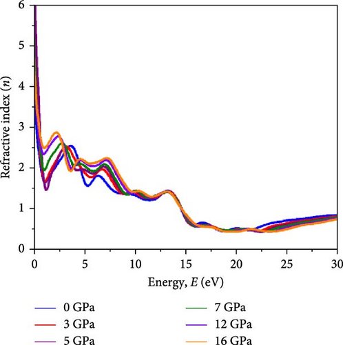
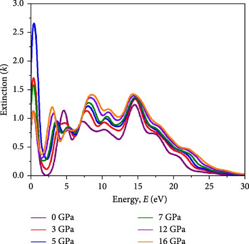
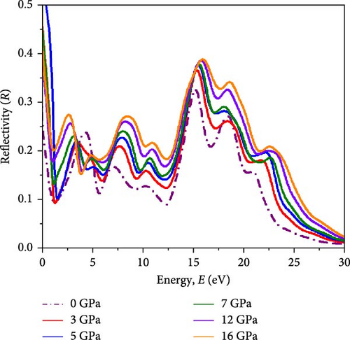
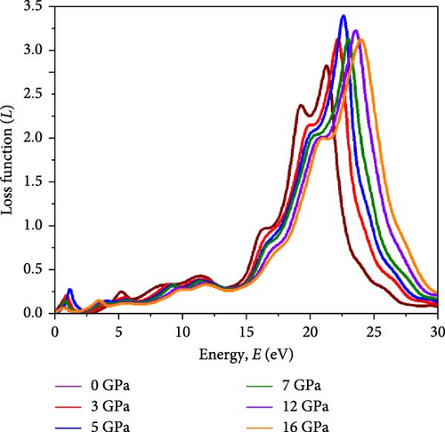
Light propagation behavior with the phase velocity of the incident wave in the absorber medium is governed by refractive index n(ω), while the extinction coefficient k(ω) determines how strongly the material absorbs or scatters light and transmits light through the materials. Figure 7a,b represents the n(ω) profile and k(ω) profile under varying pressure conditions for the Cs2HfInBr6 perovskite. A higher refractive index aids in trapping light within the perovskite material through total internal reflection, while a higher extinction coefficient contributes to enhanced light absorption and reduced transmission. The real part of the refractive index is primarily influenced by the RDC, resulting in identical dispersions between n and ε1(ω) shaped by the equation (Supporting Information Equation (14)). Illustrated in Figure 7a, the refractive index (n) reaches its highest peaks at low energies (2–3 eV), progressively decreasing in the high-energy region up to 20 eV, and then stabilizing at all pressure conditions, indicating maximal refractive index at low photon energies for these perovskites. Among all different applied pressure, highest value for n(ω) is observed at 16 GPa, gradually increasing from 0 GPa. A higher static refractive index () greater than 3 suggests that the noble Cs2HfInBr6 perovskite has strong light–matter interactions, potentially leading to enhanced light trapping, and total internal reflection, which can offer advantages in sophisticated optical devices such as waveguides and photonic crystals [72]. The extinction coefficient k(ω) as depicted in Figure 7b signifies the material’s light absorption capability and photon wave propagation depth through the material, reflecting energy absorption and dissipation. The extinction coefficient (k) peaks at the absorption maximum before declining as material absorption decreases in Figure 6c. Notably, the square root relationship with the dielectric allows for a large negative RDC, resulting in a substantial imaginary refractive index at zero photon energy. This phenomenon enables the material to strongly weaken and reflect electromagnetic waves, even without significant absorption, as illustrated in Figures 6b and 7b,c. The reflectivity R(ω), elucidating the material’ s surface optical behavior, is a crucial optical parameter for materials in photovoltaic and other optoelectronic applications. Simultaneously, the optical loss function (OLF) L(ω) delineates the energy dissipation of electrons in photon interactions. The profiles of R(ω) and L(ω) under applied pressure for Cs2HfInBr6 are evaluated using the relations (Supporting Information Equations (13) and (14)) and depicted in Figure 7c,d, respectively. High reflectivity in optical materials can lead to the loss of incident photons, reducing device efficiency. Therefore, the reflectivity profile assists in designing fabrication strategies to minimize photon losses and enhance light absorption in devices. Under visible photon exposure, the Cs2HfInBr6 double perovskite exhibits reflectivity of ~9% at 0 GPa, maintaining around 10% reflections up to 5 GPa, and experiences an increase to 20% reflectivity at 16 GPa as shown in Figure 7c. Upon transitioning to the ultraviolet region, the perovskite phase displays its highest reflectivity peak at ~15 eV, corresponding to the real dielectric function ε1(ω) in Figure 6a. The relatively lower reflectivity at low energy regions, both with and without pressure, suggests the potential of Cs2HfInBr6 perovskite for solar absorber, light harvesting applications, and as a coating material, given its higher reflectivity at high energy regions. As portrayed in Figure 7d, photon energy loss due to electronic excitations in Cs2HfInBr6 indicates that most photon energy losses occur in the UV region. In the low-energy regions, the loss function is consistently below 0.25 under all pressure conditions, while in the high-energy region, the loss function decreases with applied pressure.
3.6. Mechanical Properties
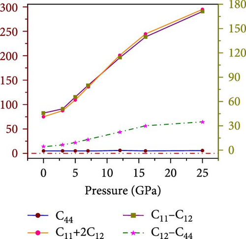
The mathematical representation of elastic constants bridges the mechanical and dynamic traits of materials, influencing their behavior under external forces and finding applications in diverse fields. The elastic tensor Cij of a crystal offers a detailed understanding of its mechanical stability, structural integrity, and mechanical characteristics. A material’s capacity to deform under stress and return to its initial configuration after removing the load defines its elastic behavior. Anisotropic behavior, binding between neighboring atomic planes, and the material’s general structural stability can all be understood by looking at elastic constants. To comprehensively describe the mechanical properties of a cubic HfIn-based halide perovskite compound under varying pressures, three independent components of the elastic tensor, namely, C11, C12, and C44 and the Cauchy pressure (C12-C44), are calculated using the finite strain theory within the first-principle DFT calculations. The elastic constants and pertinent mechanical parameters of cubic Cs2HfInBr6 double perovskite are detailed in Table 3 [73] and the material’s mechanical behavior is portrayed in Figure 8. The variations in elastic tensors indicate a consistent increase in these constants with the progressive application of pressure. This upward trend is likely attributed to the enhancement of B–X interactions within the 0–25 GPa range, in effect of strengthening lattice confinement corroborated by the observed variation in lattice constants under pressure, as depicted in Figure 2b. The computed elastic constants, in accordance with the established Born stability criteria illustrated in Figure 8a, affirm the mechanical stability of the investigated compound under applied pressure. The material’s ductile-brittle nature is primarily evident through variations in Cauchy pressure (C12-C44), representing the pressure-average shear stress nature. Figure 8a demonstrates a positive Cauchy pressure in each case, signifying the material’s ductility. The observed trend suggests that increasing pressure enhances the material’s ductile characteristics, making it more prone to plastic deformation without fracture.
| Parameters | p = 0 GPa | p = 3 GPa | p = 5 GPa | p = 7 GPa | p = 12 GPa | p = 16 GPa | p = 25 GPa | |
|---|---|---|---|---|---|---|---|---|
| C11 | (GPa) | 55.70 | 63.67 | 80.13 | 98.97 | 143.03 | 174.72 | 212.30 |
| C12 | 9.65 | 12.19 | 14.74 | 19.13 | 28.70 | 34.89 | 40.99 | |
| C44 | 5.15 | 5.52 | 5.43 | 5.87 | 6.78 | 4.99 | 6.35 | |
| C12–C44 | 4.5 | 6.67 | 9.31 | 13.26 | 21.92 | 29.90 | 34.64 | |
| B | 25.33 | 29.35 | 36.53 | 45.74 | 66.81 | 81.50 | 98.09 | |
| G | 10.00 | 10.83 | 12.23 | 14.20 | 18.71 | 18.38 | 24.08 | |
| Y | 26.49 | 28.93 | 33.03 | 38.60 | 51.33 | 51.28 | 66.78 | |
| Tm | 882.19 | 929.29 | 1026.57 | 1137.91 | 1398.31 | 1585.60 | 1807.69 | |
| (B/G) | 2.53 | 2.71 | 2.98 | 3.22 | 3.57 | 4.43 | 4.07 | |
| ʋ | 0.33 | 0.34 | 0.35 | 0.36 | 0.37 | 0.39 | 0.39 | |
| A | 0.22 | 0.21 | 0.17 | 0.15 | 0.12 | 0.07 | 0.07 | |
| Vm (m/s) | 1518.80 | 1570.08 | 1578.60 | 1639.39 | 1750.97 | 1479.15 | 1727.94 | |
| ΘD (K) | 118.96 | 142.32 | 145.98 | 153.94 | 169.33 | 145.66 | 173.89 | |
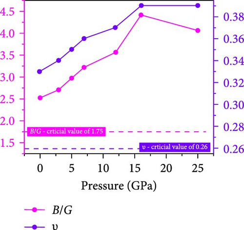
Utilizing the determined single-crystal elastic constants, the mechanical parameters of the Cs2HfInBr6 halide perovskite’s polycrystalline form are tabulated in Table 3, evaluated through Voigt–Reuss approximations [74]. In accordance with Hill’s theory, bulk (B) and shear (G) modulus for the considered perovskite exhibit elevated values, indicative of higher crystal strength against both compression strain and shear deformation. Increased pressure correlates with increased magnitudes for both parameters, as illustrated in Figure 8b as the B/G–Pugh’s ratio variations for the perovskite indicate ductile characteristics, surpassing the critical threshold of 1.75. This observation suggests that the applied pressure consistently enhances the ratio, affirming the ductile nature of the material. Quantifying resistance to longitudinal tension via Young’s modulus (Y) using B and G values reveals that increasing pressure results in higher Young’s modulus, signifying greater stiffness and reduced deformation under stress, affirming the suitability of the noble Cs2HfInBr6 double perovskite for structural integrity and diverse applications, including electronics and structural materials.
The Poisson ratio (ʋ) in perovskites describes the material’s tendency to contract laterally when compressed longitudinally, and brittle to ductile transition occurs at 0.26. Perovskite crystals demonstrate diverse phonon behaviors on specific crystal orientations, with (112) exhibiting shear and quasi-shear phonons and (100) tending only to longitudinal phonons [75]. This influences crystal orientation and phonon generation, resulted in thermal expansion coefficients or deformation potential along crystal axes, contributing to our understanding of the Poisson ratio. Cs2HfInBr6 double perovskite exhibits ductility at ambient pressure (0.33) as in Figure 8b, which increases to 0.39 at 25 GPa, reflecting the crystal’s ability to deform without fracture, indicative of a favorable atomic structure for plasticity. This observed behavior suggests potential fabrication suitability in thin film optoelectronics, flexible electronics, or structural phase change materials [75, 76].
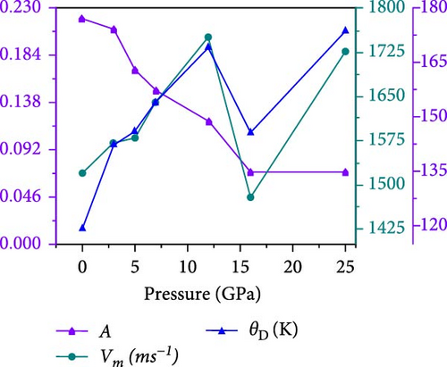
Anisotropy influences directional mechanical properties, while average sound velocity impacts electronic and photonic device efficiency, and the Debye temperature characterizes maximum atomic vibration energy, aiding thermal management in electronics. The synergistic interplay of these factors is essential in designing perovskite-based devices with optimized mechanical, electronic, and thermal properties, advancing applications in electronics, photonics, and energy conversion. The anisotropic index in perovskite crystals, impacting stress, strain, and bonding strength along crystallographic planes, is quantified by the Zener anisotropy factor (A) for the cubic Cs2HfInBr6 halide perovskite, as detailed in Table 3. The decreasing Zener anisotropy factor (A) from 0.22 at 0 GPa to 0.07 at 25 GPa, as portrayed in Figure 8c, indicating nonunity, suggests a transition toward anisotropic elastic behavior in the material. This implies potential mechanical strength and ductility improvements, supported by Cauchy pressure and B/G behavior, as shown in Figure 8a,b. Reduced anisotropy in Cs2HfInBr6 under pressure enhances its potential as an energy absorber material for high-pressure conditions, as observed in Figure 8c, with implications for pressure-sensitive devices like sensors or switches. This pressure-tunable mechanical anisotropy opens possibilities for the Cs2HfInBr6 in designing metamaterials, potentially including negative compressibility or cloaking. The anisotropy reduction under pressure may improve optical, thermoelectric, and energy storage device performance, ensuring uniform stress distribution and potentially enabling pressure-controlled LEDs or lasers for diverse applications like displays, optical communication, and biosensing.
The variations in calculated average velocity (vm) and debye temperature (ΘD) are illustrated in Figure 8c under applied pressure of 0–25 GPa for the HfIn-based cesium-bromide double perovskite. The Debye temperature data in Table 3 for Cs2HfInBr6 perovskite reveal a nonlinear trend, where values ascend from 118.96 K (0 GPa) to 173.89 K (25 GPa). This suggests a pressure-driven elevation in the average vibrational energy within the crystal lattice with Debye hardness, implying improved thermal conductivity and optimal device efficiency. The calculated mean velocity of sound (vm) in Cs2HfInBr6 perovskite is the highest at 1727.94 m/s, exhibiting a pressure-dependent increase from 1518.80 m/s at 0 GPa to 1750.97 m/s at 12 GPa and a slight decrease at 25 GPa as in Table 3. This variation implies a positive correlation between pressure and longitudinal acoustic velocity, influencing the material’s lattice dynamics and having implications for device design relying on acoustic properties. However, Table 3 also displays the estimated melting temperatures (Tm) for the perovskite under different pressures using the C11 value. The data indicate that ambient temperatures can be employed to manufacture perovskite compounds. The melting temperatures show a coherent trend, increasing from 882.19 to 1807.69 K as pressure rises. This behavior is consistent with principles of phase transitions, where higher pressure leads to a more ordered lattice structure, demanding elevated temperatures for the solid-to-liquid transition. The compression-induced stronger atomic interactions require increased thermal energy for bond breaking during melting. These insights into pressure-dependent melting temperatures are valuable for industrial applications in high-pressure environments.
4. Solid-State Photoelectric Device Characteristics of Cs2HfInBr6
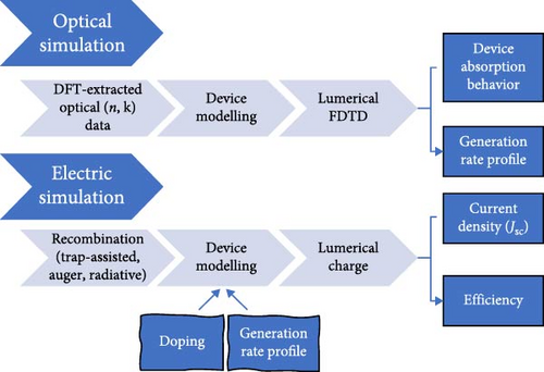
The outstanding light–matter (electron and spin) interactions through tunable quantum-confined lattice dynamics, coupled with the inherent structural stability in inorganic metal halide perovskite materials, broaden their prospective applications from advanced photovoltaic opto-spin-electronics to neuromorphic transistors and even encompass in the realm of superconductivity and correlated electronic physics applications [77–81]. In pursuit of promoting the practical applicability and as alternatives to Pd-based standard perovskites in energy conversion photovoltaic devices, particularly for achieving higher photoelectric efficiency (PCE), this study primarily entailed the modeling of a solid-state solar cell incorporating noble Cs2HfInBr6 perovskite as a light absorber layer. Henceforth, the development of the Cs2HfInBr6 halide PSC device architecture is processed through planar n-i-p heterojunction, meticulously considering the constraints outlined by the Shockley–Queisser limit [49, 74]. The device configuration comprises the top electrode of 40 nm Au, the p-type HTL of 50 nm Spiro-OMeTAD, the light-absorbing perovskite layer as 600 nm Cs2HfInBr6, the n-type ETL of 50 nm CdS, and the bottom photoanode conductive material as of 100 nm ITO, as delineated in Figure 1c. In solid-state PSCs, incident light induces the emission of photo-generated electrons, forming excitons, and the perovskite’s small exciton binding energy results in exciton dissociation into free electrons and holes, serving as charge carriers. The directional migration of charge carriers to transport layers governs their trajectory toward the anode and cathode, induced by light absorption and exciton generation. It ultimately culminates in generating an electric current integral to the overall photoelectric behavior within the PSC. Noteworthy, leveraging the morphological superiority and improved electron extraction efficiency achieved by minimizing leakage current and charge recombination at the ETL/perovskite interface and CdS is opted as the ETL in the device, with the electrode and HTL materials chosen based on relevant literature findings [82–84]. Aligned with the device behavior simulation depicted in Figure 1d and leveraging physical data extracted through DFT for perovskite materials, a FDTD approach was employed to extract key physical parameters, including light absorption and carrier dynamics, to evaluate the light-trapping characteristic of the designed device [85]. Subsequent optimizations followed by the optical trapping behavior were done to comprehend the electrical behavior of the device through a self-consistent charge transport solver in CHARGE simulations. Both FDTD and CHARGE simulations were executed using the Lumerical simulation tool.
Figure 9a represents the constructed Cs2HfInBr6 perovskite-based solar cell (PSC) solar absorption efficiency behavior under different pressure conditions. In such planar PSCs, the light absorption in PSC depends on the ETL–HTL/perovskite interface and perovskite’s own light–matter interaction behavior. As the strong absorption dependence on the refractive index behavior, we utilized the refractive index and extinction profile of the Cs2HfInBr6 perovskite calculated through DFT simulations as in Figure 7a,b. Numerous ETL–HTL optimization studies explain that thinner HTL and ETL thickness can significantly govern the device absorption behavior along with the perovskite absorber layer’s own dynamics, where excessive thickness of ETL can result in unstable absorption, causing energy losses. As light propagates from the ITO layer to the Au back contact, it experiences absorption in each layer, particularly in the Cs2HfInBr6 perovskite layer. The bandgaps and extinction coefficients of layers such as CdS, Spiro-OmeTAD, and ITO is insufficient for effective absorption of incoming light. The primary absorption occurs at the interface between the ETL (CdS) and Cs2HfInBr6 perovskite, where the bandgap of the perovskite layer is well-suited to capture the incident light. It is essential to assess the perovskite material’s potential to absorb incoming light. Figure 9a depicts the absorption curves of the perovskite absorber layer under varying pressures. It is clear from Figure 7a that at 5 GPa, the optical absorption of Cs2HfInBr6-based solar cell is smaller than the value at 3 and 7 GPa. The observed decrease in optical absorption is likely related to changes in the dielectric function. Specifically, at 5 GPa, the exciton binding energy (5.74 meV) is lower compared to 3 GPa (16.43 meV) and 7 GPa, (14.45 meV) as indicated by the dielectric function data. This lower exciton binding energy at 5 GPa can result in reduced optical absorption efficiency.
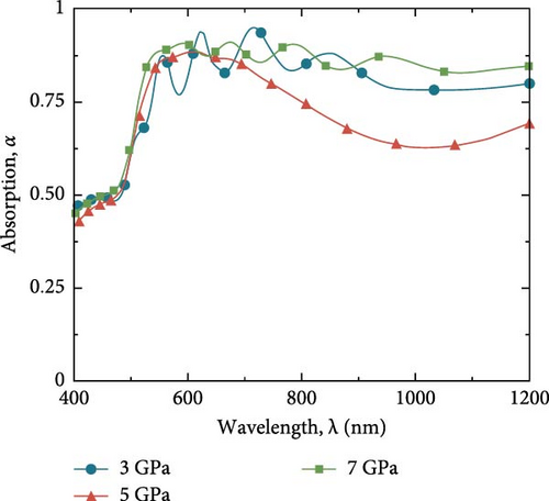
These curves demonstrate a consistent degree of absorption within the visible range of the incident light, indicating the material’s stability. The absorption values for shorter wavelengths of light are lower because shorter wavelengths penetrate less into the Cs2HfInBr6 layer. The absorption of light in the wavelength range of 550–800 nm exceeds 75%, indicating a strong capacity to capture light in the perovskite layer. This characteristic is ideal for promoting the creation of a large number of EHPs.
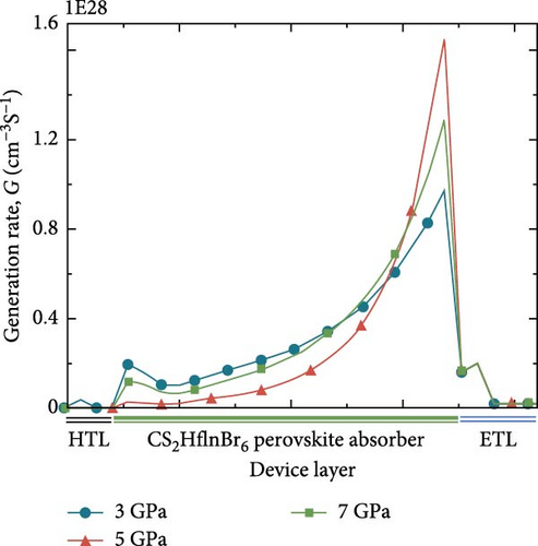
The generation rate of a solar cell is defined as the quotient of the total number of electrons generated and the volume of the device. Based on the data presented in Figure 9a, it is observed that the absorption value of the perovskite layer remains high even beyond the visible range for pressures of 3 and 7 GPa. This observation is further supported by the generation rate curves shown in Figure 9b. The generation rate within the perovskite layer is greater for Cs2HfInBr6 under pressures of 3 and 7 GPa, within the thickness range of 100 to 600 nm of the device. Due to the strong correlation between the generation rate and absorption, Cs2HfInBr6 with a pressure of 3 and 7 GPa exhibits considerably greater absorption levels beyond the visible spectrum of light. Nevertheless, the rate at which new EHPs are formed is greatest near the junction between the absorber layer and ETL. This is because perovskite Cs2HfInBr6 has a strong tendency to absorb visible light, making the process of EHP formation highly efficient.
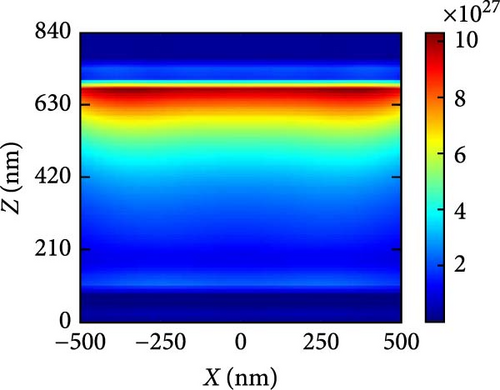
Figure 10a–c illustrates the generation rate profiles across the entire device under pressures of 3, 5, and 7 GPa of the perovskite materials. At the boundary between ETL and perovskite, the rate of generation is the highest, but it steadily drops as light penetrates further into the perovskite material at each pressure level. At a pressure of 5 GPa as shown in Figure 10b, most of the generation occurs at the upper level of the perovskite and at the interface between the ETL and absorber layer, where some exciton scattering effect is observed for other pressures as shown in Figure 10a,c. This is also readily apparent from the generation rate curves presented in Figure 9b.
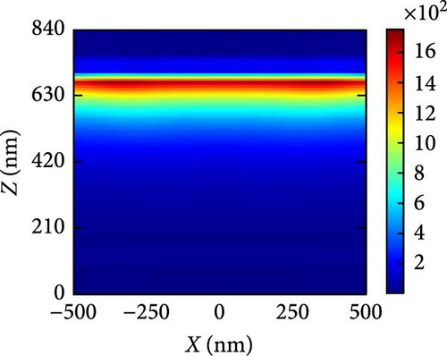
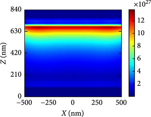
In order to explain the absorption and generation spectra of these three pressures in the perovskite, we conduct simulations of electric field intensity profiles at four specific wavelengths: 400, 600, 800, and 1000. These profiles are shown in Figure 11. Figure 11a–c demonstrates that the highest strength of the electric field (E field) occurs in the vicinity of the uppermost layer of the PSC when the wavelength of the light is at its minimum (like 400 nm). This is because short-wavelength light has a limited ability to penetrate, and the ETL layer has a low absorption coefficient in the region of low wavelengths. The electric field generates a standing wave within the perovskite layer due to the Fabry–Perrot resonance induced by the Au back reflector. This phenomenon is observed at wavelengths of 600 and 800 nm under pressures of 3 and 5 GPa, respectively. Since the generation rate for 5 GPa of the perovskite is primarily confined in its upper portion, most of the field intensity for 800 and 1000 nm light wavelengths is observed in the upper portion of the perovskite. As the wavelength of light rises, we observe a greater propensity for light to permeate deeper into the device, as longer wavelengths have a higher penetration capacity.


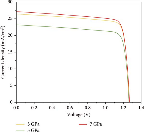
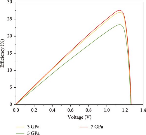
To understand the device performance with power conversion mechanism, I–V profiles and PCE are evaluated as portrayed in Figure 12. As a result of applied pressure, the open circuit voltage (Voc) shows to be decreased in 1.25 V for all three pressures, whereas the current density varies from 23 to 27 (mA/cm2) shown in Figure 12a. The PCE versus Voc characteristics show the variations by pressure for the considered perovskite in Figure 12b. It can be noticed that the 7 GPa applied pressure offers the highest PCE values compared with the counterparts. The maximum PCE of the proposed Cs2HfInBr6 DHP design is 27.5% for 7 GPa external pressure. The observed behavior in Figure 12 can be interrelated with the optical absorption and conduction profile in effect of carrier lifetime by carrier generation recombination profile as observed in Figures 6c,d and 9.
5. Conclusion
This study examines the noble halide double perovskites Cs2HfInBr6 under pressure, exploring structural, electronic, elastic, thermoelectric, and optical properties. Employing GGA–PBE, geometry optimization of Cs2HfInBr6 crystallized it into a cubic phase, showing reduced lattice parameter (a) under increasing hydrostatic pressure due to decreased lattice vacancies. The application of pressure caused tilting in the Hf–Br and In–Br octahedral framework, resulting in lattice confinement and potentially leading to a transition from semiconductor to metallic phase with alterations in direct–indirect band gap properties. With these tunable electronic behaviors, the noble Cs2HfInBr6 also demonstrates a large bandwidth optical absorption spectrum spanning from visible to high energy region under different pressure conditions. This new perovskite phase demonstrates its potential for industrial applications with hydrostatic pressure variations through mechanical stability as observed as thermodynamically. PSC FDTD simulations in later part solidify the DFT findings of the noble Cs2HfInBr6 perovskite’s potential as a promising candidate for advanced solar energy harvesting devices. These findings corroborate about the Cs2HfInBr6 as a phase-transitioning noble DHP suitable candidate for perovskite thin films, flexible solar cells, multiferroic transistor, memory, biomedical, and photovoltaic technologies.
Conflicts of Interest
The authors declare no conflicts of interest.
Author Contributions
The study was conceived by R.S.A. and N.H. Numerical calculations and data analysis were conducted by R.S.A., N.H., and M.H.K.A., and they prepared the manuscript. M.M.H., M.A., and A.K. contributed to data analysis and result interpretation. Project supervision and manuscript review and editing were carried out by M.H.R. and A.K. All authors participated in manuscript preparation, result discussion, and comment review before submission.
Funding
This work is supported by the NSU research under Grant no. CTRG-24-SEPS-06.
Acknowledgments
The authors acknowledge the Department of Mathematics and Physics of the North South University (NSU) Bangladesh for the facilities given to them to do this research work. Alamgir Kabir acknowledges the Department of Physics, University of Dhaka, for providing computational support. The denser K-point calculation was facilitated by the Computational Condensed Matter Research Laboratory of BRAC University, Dhaka, Bangladesh.
Supporting Information
Additional supporting information can be found online in the Supporting Information section.
Open Research
Data Availability Statement
The data that support the findings of this study are available at https://drive.google.com/drive/folders/1FHvkjJJ_UkWHsiRHHlcvT8lHVMaZv_5a.


