Development of CoTe2, CoS2, and CoSe2 Electrode Material for the Asymmetric Supercapacitors
Abstract
Supercapacitors play a crucial role in electrical energy storage and conversion applications today due to their high power density and ability to integrate with various energy conversion devices. Many efforts have been made to address issues such as low energy density and finding efficient electrode materials to achieve high capacitances. Layered transition metal dichalcogenides have shown great potential in energy storage applications because of their numerous active edges, diverse electrochemical kinetics, and unique sandwich structure. Therefore, researchers have been exploring a meticulous method to formulate multiscale CoS2, CoSe2, and CoTe2 nanoarchitectures to enhance the storage characteristics of supercapacitors. This study employed a single-step facile chemical reaction method to form CoSe2, CoTe2, and CoS2 nanostructures. The synthesized CoTe2 material demonstrated a specific capacity of 370 C g−1 at 1 A g−1 alongside reliable cycling robustness over 10,000 cycles (98%), superior to CoSe2 and CoS2 electrodes. An alkaline hybrid asymmetric supercapacitor based on CoTe2 achieved a 157 F g−1 specific capacitance with 56 Wh kg−1 specific energy and a long cycling life of 97% capacitance retaining over 10,000 cycles. These findings reveal the significant potential of cobalt chalcogenide nanostructures to be applied as prototype electrodes for supercapacitor devices.
1. Introduction
In the current era of increasing energy requirements, it is imperative to have resourceful energy stowage kinetics to accommodate advancements in energy harvesting and generation technologies and their regulated supply [1, 2]. Electrochemical supercapacitors offer promising pulse power delivery system solutions for various applications, such as transient response equipment, portable consumer electronics, industrial power setups, hybrid electric vehicles, and electric devices [2, 3]. Supercapacitors are gaining prominence as novel devices for energy stowage owing to their stimulating merits, such as low weight, good reversibility, short charging times, high power density, and long spam solidity [4]. Supercapacitors utilize diverse materials, including transition metal chalcogenides (TMCs)/oxides, conductive polymers, and carbonaceous materials [5, 6]. Based on the composition of these materials, two notable storage kinetics have been recognized: electrochemical double-layer capacitance (EDLC), where charges accumulate at the electrodes/electrolyte interface and pseudocapacitors, where reversible reactions facilitate charge storage [7, 8]. It is important to note that pseudocapacitors and EDLCs face certain advantages and challenges for energy storage applications. However, battery-type electrode materials can substantially produce reversible Faradaic reactions and enrich the specific capacity and energy density compared to carbon materials [9]. The advancement of hybrid supercapacitors, which integrate the advantages of both batteries and supercapacitors without compromising power density or cycle lifetime, is essential for the next generation of energy storage devices [10, 11]. The productivity of hybrid supercapacitors relies heavily on the electrode materials’ properties. Among various electrode materials, battery-like materials have become a significant focus of research due to their ability to facilitate numerous redox reactions, which enables them to deliver a desirable capacity.
Carbon-based materials are commonly used in commercial supercapacitors due to their minimal costs and high conductance, making them excellent choices for swift energy stowage applications [8, 12]. However, the short potential window and specific capacitance of supercapacitors constrain their usage in practical applications [13, 14]. The most recent studies have focused on systematically studying devices and designing efficient electrode materials to improve device construction. Consequently, there is an increasing need to discover nanomaterials that exhibit excellent conductivity, making this an essential area of focus in the advancement of supercapacitor technology [15]. Electrode components are considered a vital part of supercapacitor devices, as they govern the performance of such devices based on their electrochemical, mechanical, and physical features and composition under an electrolytic media [16]. To improve electrode properties, TMCs, such as metal tellurides, selenides, and sulfides, are exchanged as efficient electrodes; they exhibit significant advantages and features for charge storage reactions [17, 18]. TMCs inherently possess high electrical conductance with outstanding electrochemical characteristics that can be tuned into attractive nanostructures [19]. Furthermore, the electronic configuration center of TMCs can be controlled by modifying the composition, thereby altering the conductance and charge storage behavior [20]. The specific layers of TMCs protrude in a particular direction due to the fragile van der Waals interaction forces. They also reveal stacked multilayer morphology features with covalent. This enables their usage for fabricating any desired module with a tuned porosity and large surface region, which render excellent beneficial properties for energy storage processes [21]. The construction of binary TMCs has been highlighted as a feasible approach to coordinate electrochemical behaviors [19]. TMCs have been established as favorable battery-type materials because of their high conductance, electroactivity, and numerous redox active sites for supercapacitors [7, 22].
The synthesis of metal chalcogenides can yield enriched electrochemical properties associated with monometal oxides or other electrodes [23, 24]. Thus, constructing a cobalt chalcogenide-coupled battery-type material can address the aforementioned issues and help attain conducive electrochemical performance by incorporating features of the two elements. Cobalt chalcogens (CoX2) have been proposed as efficient electrodes because of their exceptional electrochemical behavior, remarkable electrical conductance, and rich redox edges [23, 25]. Extensive attention has been paid to various TMCs, including CoS2, CoTe2, and CoSe2, owing to their good electrochemical performance, improved conducting behavior, metallic nature, diverse nanostructures, and mixed valence levels [7, 21, 24]. However, these monometal chalcogenide-based supercapacitors face various hindrances, such as cycling steadiness and huge volume change by continued reactions. Tellurium (Te) shows considerable potential in this regard because of its innate metallic properties [26]. Te is a durable element and owns superior conductivity, in comparison to selenium and sulfur, which is enhanced by its lower electronegativity and larger atomic size, which together improve its electrochemical behavior [13, 27]. Te-based nanomaterials are synthesized to provide excellent electrochemical activity and expedited reaction kinetics. Younas et al. [26] have synthesized the 2D Co0.63Te electrode material which explored the 776 F g−1 specific capacitance at a current density of 2 A g−1 and better solidity of 82 % capacitance retention after 5000 cycles. Mao et al. [28] have formulated the nanoflower-shaped CoTe2 for the supercapacitor electrode and produced 460 F g−1. The p-type conductivity, low band gap of 0.35 eV, and conductivity of 10 × 103 S/m yield improved electrochemical characteristics. Despite demonstrating noteworthy gains compared to Se/S, metal Te-based materials do not primarily focus on energy storage uses. The tuned surface features of CoS2, such as nanowires, nanocages, and nanosheets, synthesized by unique procedures can significantly improve electrochemical behavior. Moreover, ordered sheet-like morphologies have shown significant merits owing to their large surface-to-bulk ratio and quicker diffusion routes for ions and electrons [29]. The selective morphologies of CoS2 can create a bulk volume extension, which reduces the capacitance and conductivity for cycling studies [22]. In addition, compared to other architecture sulfides or oxides, the developed conductivity and improved morphologies of metal selenides offer more benefits for charge stowage kinetics. An earlier study revealed that CoSe2 nanosheets showed a specific capacitance of 333 F g−1 with superb continuing solidity over 25,000 cycles [30]. An assembled asymmetric device with CoTe//AC configuration yielded a capacitance of 67.3 F/g [31]. However, the performance of cobalt chalcogenide-based electrodes needs to be improved in terms of energy, firmness, and suppleness. Synthesizing CoX2 nanostructures to accomplish efficient electrochemical storage characteristics remains a significant task. This study presented a facile single-step chemical reaction to assemble nanosheets and explore their applications for hybrid asymmetric supercapacitors. The CoTe2 material showed a 370 C g−1 specific capacity at 1 A g−1 and an admirable stability behavior with 98% maintenance after 10,000 cycles. Additionally, the fabricated asymmetric capacitor presents tremendous charge stowage behavior alongside a high specific energy of 56 Wh kg−1 at the specific power of 2.25 kW kg−1, which outperforms outcomes from previous literature.
2. Experimental Details
2.1. One-Step Preparation of CoX2 Nanostructures
A facile single-phase kinetics followed through annealing was utilized to form the CoX2 nanostructures [32]. To develop the CoTe2 nanostructure, a chemical reaction was initiated between ammonium cobalt sulfate ((NH4)2Co(SO4)2) and Te dioxide (TeO2). Initially, TeO2 (0.05 M) was liquified in a blend (100 mL) of 5% sulfuric acid and 95% deionized water (DI), followed by heating at 90 °C for 2 h. The final form of the homogeneous solution was used for reaction kinetics. Then, the equipped solution was combined with a (NH4)2Co(SO4)2-dissolved solution under active magnetic blending for 1 h. Thereafter, 20 mL hydrazine hydrate (N2H4) and 10 mL ammonium hydroxide (NH4OH) were slowly combined successively with continual magnetic blending to prepare a homogeneous bath. The resultant mixture was then moved to an 80°C hot plate for 3 h with magnetic blending. The subsequent precipitant was gathered and cleaned in a centrifuge with ethanol and DI water. Lastly, the black CoTe2 nanopowder was subjected to heating in an oven for 3 h at 60 °C, followed by annealing in a Te environment for 2 h at 500°C. To prepare CoSe2 and CoS2 nanostructures, selenium dioxide (0.1 M in 100 mL) and thiourea (0.5 M in 100 mL) were dissolved in DI, respectively, followed by the magnetic blending of the (NH4)2Co(SO4)2 mixture at room temperature (~30°C) for 1 h. Thereafter, N2H4 and NH4OH solutions were dropped slowly into the mixture. After attaining the homogeneous mixture, the same procedure was followed as described for preparing CoTe2. The extracted black-colored CoX2 nanostructures were desiccated for further analysis.
3. Supercapacitor Studies
Fabricated CoX2 electrodes were employed to assemble supercapacitor devices. To construct the active electrode, the synthesized CoX2 nanomaterials were initially integrated with Nafion solution. Then, the resulting ink was drop-casted on precleansed nickel foam (NF) with the dimension of 1 cm2 and parched for 12 h at 80°C. The uniform 3 mg active material was coated on NF for all the nanomaterials. For the three-electrode mode, 3 M KOH was used as an electrolyte with Hg/HgO and Pt as a reference and counter electrode, respectively. For the asymmetric experiment, Whatman paper, soaked for 8 h with 3 M KOH, was inserted between the two similarly sized negative and positive electrodes. The positive and negative electrode was prepared material and activated carbon-loaded NF, respectively. The electrochemical impedance and cyclic voltammetry (CV) studies were recorded using the PARSTAT (PMC-1000). Furthermore, the galvanostatic charge–discharge (GCD) was acquired using the ZIVE SP1 unit.
4. Results and Discussion
An easy chemical reaction was utilized to realize the CoX2 (CoSe2, CoS2, and CoTe2) nanostructures. Figure 1 is a schematic showing the preparation of CoX2 nanostructures through the proposed methodology and their atomic arrangements. Initially, the Raman scattering tool was used to confirm the construction of CoSe2, CoS2, and CoTe2 nanostructures. Then, field-emission scanning electron microscopy (FESEM) analysis was employed to identify the morphological characteristics of the CoX2 nanoclusters. Figure 2 demonstrates the FESEM images of the CoSe2 nanostructures. The elevation of ordered sheet-like grains with various domain shapes was explored in the low magnification image, as shown in Figure 2a. The exhibited high-resolution image (Figure 2b) shows that the aggregated nanocuboids tended to form grain domains for CoSe2. Figure 2c shows a high-resolution FESEM image depicting obliquely stacked sheet-like grain domains within the CoSe2 clusters. Additionally, Figure 2d displays the FESEM mapping image of CoSe2 nanosheets, which produced homogeneously dispersed elements. Figure 2e,f shows the distribution of the Se and Co elements on the CoSe2 nanosheet domain, confirming the equal circulation of all the kernels on the domain. Figure 2g shows the energy dispersive spectrum (EDS) of CoSe2 nanodomains, which helped us explore the composition of the constructed nanosystems.
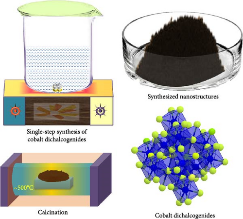
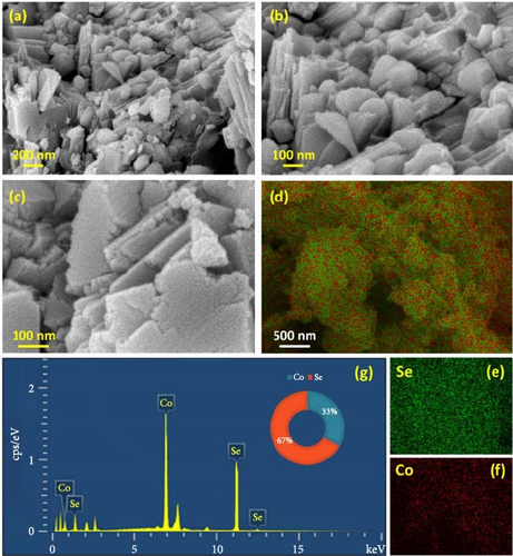
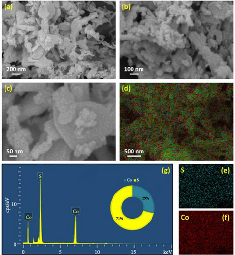
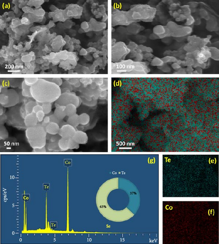
Figure 3a–c demonstrates the FESEM images of the CoS2 nanostructures. The presence of spherical-shaped grains agglomerated with wrinkled sheets of domains can be seen in Figure 3a. Figure 3b illustrates a high-magnification micrograph describing the aggregation of nanospherical particles forming nanodot-shaped grain domains for CoS2. Figure 3c shows the high-resolution FESEM micrograph depicting the dispersal of the nanodots over the crumpled sheet CoS2 domains. The elemental mapping image of CoS2 nanosheet-like domains is shown in Figure 3e. Figure 3e–f reveals the distribution of the S and Co elements on CoS2. The detected results elucidate the equal spreading of S and Co components in the CoS2 domain. Figure 3g shows the EDS profile of CoS2 nanodomains, which helped us explore the assembled nanostructure composition. Figure 4a–c displays the FESEM images of the CoTe2 nanostructures. The spherical-shaped grains were agglomerated for the CoTe2 nanostructures, as shown in Figure 4a. Further, the high-resolution images (Figure 4b,c) reveal the cluster decorated with nanospherical grains. A substantially unified grain cluster influenced the morphological assembly of large-sized grain domains. Figure 4d exhibits the constituent mapping of the CoTe2 nanomaterials. The fragment mapping contour influentially establishes the consistent dispersal of Co and Te components, as demonstrated in Figure 4e,f, respectively. Figure 4g displays the EDS profile of the CoTe2 nanostructures. The composition profile of the CoTe2 nanostructures reveals 63 at% of Te and 37 at% of Co.
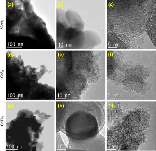
The atomic organization of the synthesized CoX2 structures was studied by high-resolution transmission electron microscopy (HRTEM) experiments. Figure 5 displays the HRTEM images of the prepared CoX2 structures. A large-area HRTEM profile defined the agglomerated large-sized grains in the CoSe2 nanostructures (Figure 5a). Figure 5b shows the nanocuboid shape of the accumulated grains for the CoSe2 nanostructures. The high-resolution HRTEM profile (Figure 5c) of the CoSe2 nanostructures helped us explore the distinct lattice direction with the interfaced grain domains for the CoSe2 nanostructures. Figure 5d–f shows the different magnification HRTEM profiles of the CoS2 nanostructures. For the CoS2 nanostructures, the wrinkled shapes of the sheet-like structures with the undefined grain domains were explored. The high-resolution profiles (Figure 5e,f) elaborate the interfaces of the lattice direction with definite atomic scale arrangements in the CoS2 nanostructures. The combined bulk sizes of the grain domains are shown in the HRTEM image of the CoTe2 nanostructures (Figure 5g). A selective shape of a larger-size domain shows the contribution of fingerprint-like lattice on the surfaces of the CoTe2 nanostructures (Figure 5h). Figure 5i exhibits the well-positioned and well-organized thumbprint-like perpendicularly united fringes due to the structured arrangement of the atoms. The observed microscopy FESEM and HRTEM results correlated strongly with each other to form the CoX2 nanostructures.
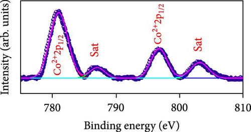
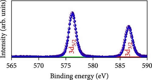
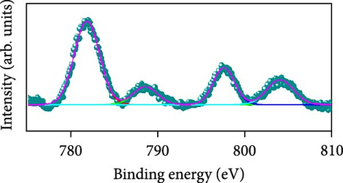
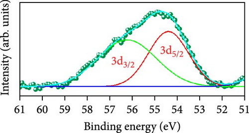
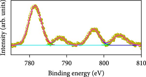
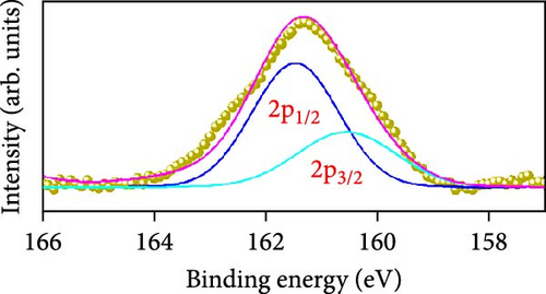
Raman scattering was conducted to authorize the physical confirmation of the derived nanostructures. Figure 6a–c displays the Raman shift of the CoS2, CoSe2, and CoTe2 nanostructures, respectively. From pure CoS2, the diffraction peak was between 284 and 386 cm−1, correlating to in-phase Ag and out-of-phase stretching Tg vibration of the sulfur atoms, respectively [33, 34]. The 2D characteristic Se−Se stretching mode of the CoSe2 nanostructure originated at 190.1 cm−1 [35, 36]. The pathetic broad peak is detected at around 250 cm−1 owing to the amorphous nature of Se [37]. The Raman spectrum reveals the vibrations at 122 cm−1 and 291 cm−1, which was due to the A1g and E2g modes of the CoTe2 nanostructures, respectively [38, 39]. To explore the oxidation states and chemical constituents, an X-ray photoelectron spectroscopy (XPS) examination was carried out for the CoX2 nanostructures. Figure 6d displays the Co 3d binding energy XPS profile of the CoTe2 nanostructures. The observed signal signifies the two-shakeup satellite (sat) peaks and spin–orbit doublets in the Co 3d region. The observed spin–orbit contributing to the binding energies of 780.3 and 797.5 eV was credited to the 2p3/2 and 2p3/2 states, respectively [40, 41]. Figure 6e shows the Te 3d region of the CoTe2 nanostructures. Deconvolution proved the robust duos for the CoTe2 nanostructures at 576.8 and 587.1 eV and the binding energy owing to 3d3/2 and 3d5/2, respectively [42]. Figure 6f displays the Co 3d region which produced the duos at 780.9 and 797.2 eV owing to 2p3/2 and 2p1/2, respectively, along with the sat peaks for CoSe2 [43, 44]. The Se 3d region was bound with a couple of peaks of 3d5/2 and 3d3/2 at 56.3 and 54.2 eV, respectively, which were also consistent with CoSe2 (Figure 6g) [45]. Figure 6h reveals the spin–orbit coupling and sat peak for the CoS2 structure. The XPS profile of the S 2 p region (Figure 6i) exposed divalent bonds at 161.9 and 160.5 eV corresponding to 2p1/2 and 2p3/2, respectively, for CoS2. The observed XPS results strongly proved the formulation of the CoX2 nanostructures.


The surface characteristics of the CoX2 nanostructures were examined through nitrogen (N2) sorption scans via the Brunauer–Emmett–Teller (BET) procedure. Figure S1a displays the N2 sorption shapes of CoSe2, CoS2, and CoTe2. The observed profile reveals the type-IV standard. High pressure enabled swift sorption kinetics owing to their mesoporous nature. The surface areas obtained were 2.6, 2.3, and 3.9 m2· g−1 for CoSe2, CoS2, and CoTe2, respectively. The enhanced BET area of CoTe2 was recognized as the absolute metallic feature of the inserted chalcogen atom. The formulated CoTe2 matrix initiated a high surface area, enabling a large region of reachable and abundant active edges to be associated with their similar modules of CoS2 and CoSe2 structures. Active facets indicate to definite spots within the electrode material where ions are adsorbed and redox reactions occur. A larger surface area can provide more contact points for ion adsorption, which may enhance overall electrochemical performance by increasing the availability of these active sites for energy storage. Active sites serve as binding points for ions from the electrolyte, enabling their storage within the electrode material and facilitating their involvement in electrochemical reactions. This facilitated a swift reaction mechanism between the electrolyte/electrode sites [46]. Figure S1b shows the Barrett–Joyner–Halenda contours of the CoX2 structures. The obtained pore diameter and volume values were assumed to be the mesoporous nature of the formulated CoX2 structures. The estimated mean pore diameters were 13, 12, and 30 nm for CoSe2, CoS2, and CoTe2, respectively. The improved pore diameter of the CoTe2 particles can be attributed to the commitment of abundant active faces on the operating region. The derived pore diameter, pore volume, and BET area values are provided in Table S1.
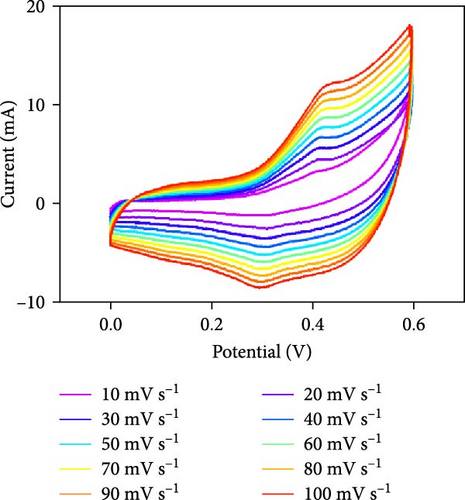
Three-electrode electrochemical experiments were performed to demonstrate the electrochemical stowage properties of the synthesized CoSe2, CoS2, and CoTe2 electrodes. The CVs of CoSe2, CoS2, and CoTe2 electrodes at 100 mV s−1 with 0–0.6 V potential are shown in Figure 7a. From the experimental results, the redox duos of CoSe2, CoS2, and CoTe2 electrodes were discovered, implying the battery-like performance for charge storage kinetics. Furthermore, the CV profile of the CoSe2 spherical-structured electrode created a redox peak due to its battery-type behavior and improved the storage characteristics compared to the CoS2 and CoSe2 results, signifying a plentiful catalytic facet with rapid conducting performance and leading to superior capacitance. The high potential swing of the oxidation peaks and low potential swing of the reduction peaks in terms of the scan rate were due to the enrichment of the inner diffusion resistance of the material [47]. The enrichment of redox intensity in terms of the scan rate was significantly recognized for all the CoX2 electrode materials, thus demonstrating their high-speed competence for electrochemical stowage. The obtained robust redox peaks could be initiated via the association of distinct valence states of Co [48]. Therefore, the designed CoX2 material energy stowage process can be followed by the given kinetics [49]:
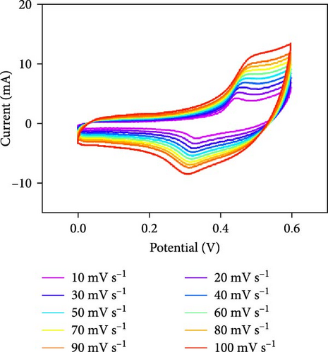
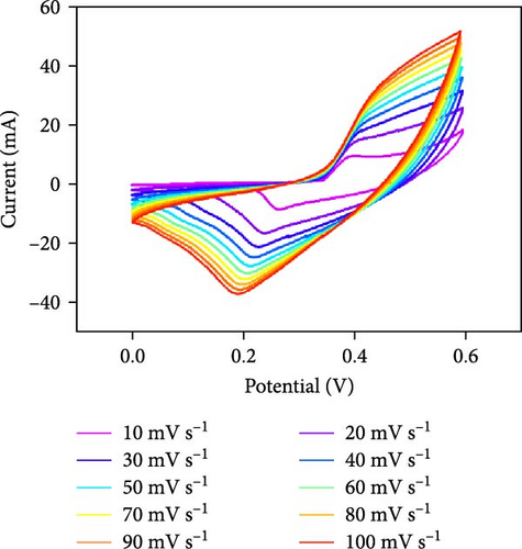
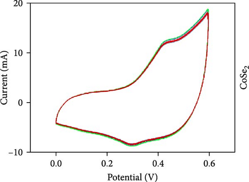
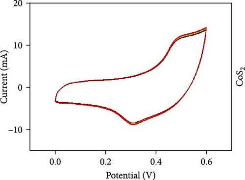
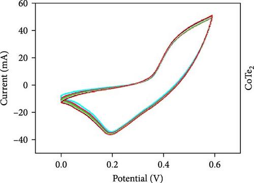
To realize the electrochemical solidity of the formulated CoX2, cycling studies were carried out for the assembled supercapacitor electrodes, as illustrated in Figure 7d–f. The results established robust Faradaic kinetics and remarkable retentivity over 100 CV cycles for all the organized materials. From the observed electrochemical characteristics of the CoTe2 structures, admirable redox kinetics could emerge from the ensuing features; the mesoporous nature surface can shorten the ion transference path with high mechanical properties, which can sustain a stable microstructure for prolonged span of the cycling measurement. Additionally, the metallic electrical conductivity of Te offers superior storage activity [27, 50].
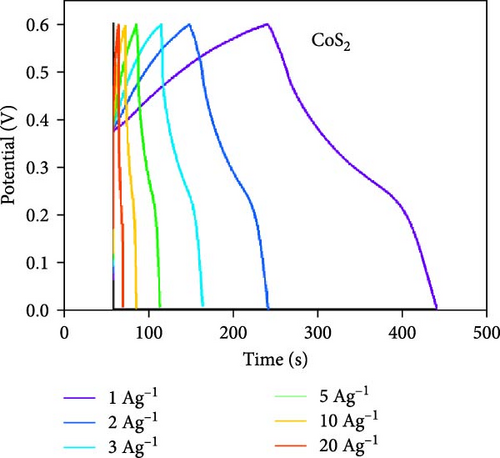
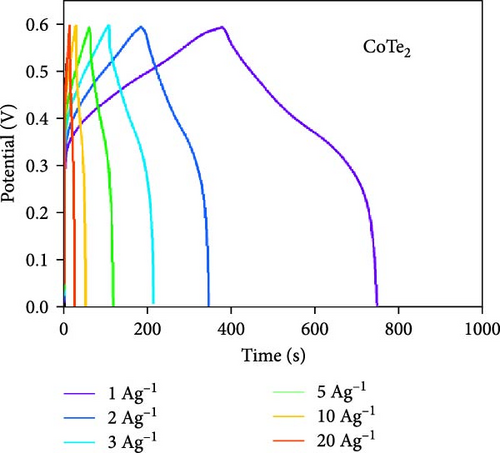
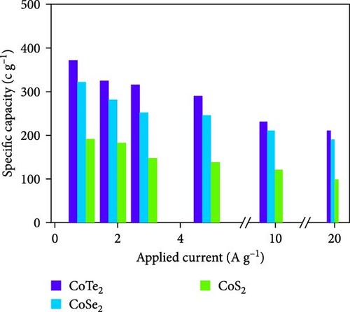
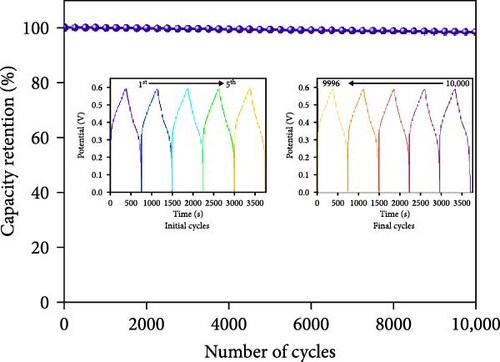
Moreover, GCD studies were carried out to define the energy stowage kinetics of the prepared CoX2 materials by the three-electrode mode. Figure 8a–c shows the various utilized currents employing the examined GCDs of CoSe2, CoS2, and CoTe2 electrodes for the 0–0.6 V potential range. The nonlinear GCD profile demonstrated strong batter-type electrochemical stowage features for all the prepared materials [51]. The identified GCDs specified the sustained charging/discharging period of the prepared CoTe2 electrode, which was consistent with the CV results. Figure 8d shows the specific capacity variation for the CoSe2, CoS2, and CoTe2 electrode materials. The calculated specific capacities of the CoSe2, CoS2, and CoTe2 supercapacitor electrodes at 1 A g−1 applied current were 216, 143, and 283 C g−1, respectively. The estimated capacity outcomes reveal the enhanced storage properties of the CoTe2 material compared to their equivalent structures. The assembled CoTe2 nanostructure induced enriched stowage capacities of 370, 324, 315, 290, 230, and 210 C g−1; the CoSe2 material offered 321, 280, 252, 245, 210, and 190 C g−1; and CoS2 offered 191, 182, 147, 138, 120, and 98 C g−1 at applied currents of 1, 2, 3, 5, 10, and 20 A g−1, respectively. The high specific capacity of the CoTe2 nanostructure could be qualified to diverse factors, such as its highly porous nature and spherically shaped dense nanodots, enabling an enriched surface area to support the rapid de-intercalation/insertion of KOH ions. The capacity values gradually decreased with an increase in the amount of applied current, which could be attributed to the involvement of deficient active materials for redox kinetics, as the diffusion span was restricted for active materials for retrieving the ions of electrolyte at high charge–discharge speeds [52, 53]. Moreover, the metallic conductivity of CoTe2 induced a high electrical conductance, and the extended lattice spacing between the specific CoTe2 fringes permitted the superficial intercalation/de-intercalation of the electrolyte ions. The outstanding electrochemical behavior obtained could be credited to the fast charge transport ability and swift electrical conductivity of the electrode materials. Figure 8e exhibits the electrochemical impedance spectroscopy (EIS) graphs of the CoSe2, CoS2, and CoTe2 battery-type electrodes. The extracted electrical circuit inserted in Figure 8e defines the contact resistance (Rct) of 24, 21, and 18 Ω for the CoSe2, CoS2, and CoTe2, respectively. The initial resistance (Rs) is exhibited at 2.4, 2.3, and 1.8 Ω for the CoSe2, CoS2, and CoTe2, respectively. The identified EIS determined the short resistance type of the prepared CoX2 electrodes, which could be attributed to the intense relations between the electrode materials and current collector and enriched morphological features [54]. The long-term cycle capabilities of the CoSe2, CoS2, and CoTe2 electrodes were measured for 10,000 cycles. Figures 8f and S2–S3 show the cycling studies of CoTe2, CoS2, and CoSe2, respectively. The profiles explored the steady state of specific capacity over 10,000 cycles with 98% of the original capacity for the CoTe2 electrode, whereas CoS2 and CoSe2 produced 94% and 97% of retention capacities, respectively. The initial and final five cycles (inset of Figure 8f) of GCDs were almost symmetrical for the CoTe2 electrode, thus confirming outstanding structural solidity and reversibility [55]. The enhanced cycling performance could be attributed to the following reasons. First, its high surface area and voids and nanodot surfaces offered sufficient free area to lodge the large volume of KOH ions during the GCD mechanism. Second, the abundant mesoporous nature, highly available surface active sites, and inherent electrochemical solidity helped the CoTe2 matrix to not collapse during the GCD kinetics [52].


Asymmetric devices were constructed by inserting a 6 M KOH-dipped Whatman filter paper between CoX2 and activated carbon as positive and negative electrodes to establish their commercial applications (Figure 9a). The mass calculation between the negative and positive electrodes was performed using the following relations [56]:
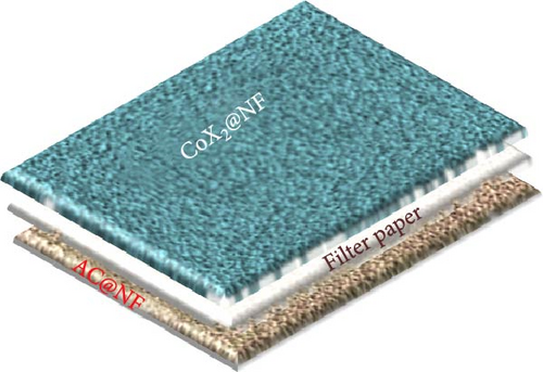
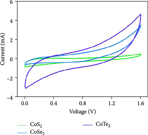
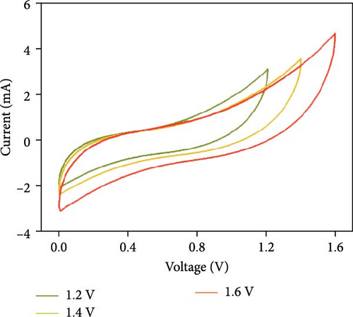
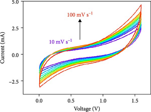
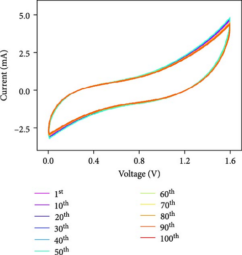
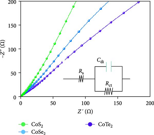
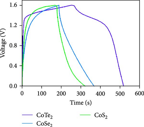
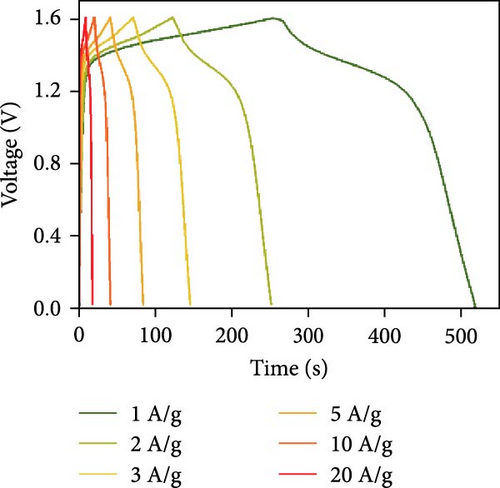
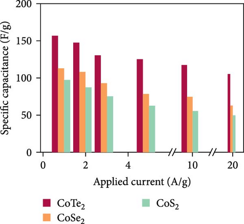
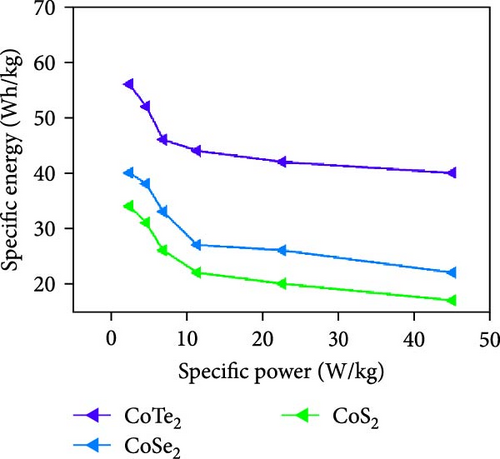
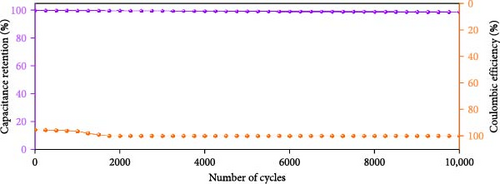
Figure 10d indicates the Ragone profiles of the asymmetric capacitors using the CoTe2, CoS2, and CoTe2 positrodes. The calculations revealed the ultimate specific energy values of 56, 52, 46, 44, 42, and 40 Wh·kg−1 for CoTe2; 34, 31, 26, 22, 20, and 17 Wh·kg−1 for CoS2; and 40, 38, 33, 27, 26, and 22 Wh·kg−1 for CoSe2 at specific power values of 2.25, 4.5, 6.75, 11.25, 22.5, and 45 kW.kg−1, respectively. The obtained results of CoTe2 were higher than those of the synthesized materials of CoS2 and CoSe2 and the reported literature, including Ni3Se2//AC (22.3 Wh kg−1) [59], CoSe2//AC (18.9 Wh kg−1) [55], CoSe//AC (18.6 Wh kg−1) [60], Co0.85Se//N-PCNs (21.1 Wh kg−1) [61], CuCo2Se4//AC (9.45 Wh kg−1) [62], NiMoS4-A//AC (35 Wh kg−1) [52], CF@CoTe2-NiTe2//CF@Fe2O3 (41 Wh kg–1) [27], Co9S8 nanoflakes//AC (31.4 Wh kg−1) [63], NiTe//AC (33.6 Wh kg–1) [64], and CoMoS4//rGO (27.2 Wh kg−1) [65]. The observed results show that the modified nanodot surface features of the synthesized CoTe2 positrode are highly capable of accommodating a large volume of ions within their lattices, thus offering more accessible sites for improved device characteristics [56]. Figure 10e shows the cycling behavior and coulombic efficiency of the asymmetric capacitors with the CoTe2 material at 20 A g−1. During the GCD cycling, the ions gradually penetrated to the electrode system, strengthening the interaction area and bettering ion transportation and transmission to the interior layer. The examination confirmed the maintenance of 97% of the original capacitance after 10,000 cycles for CoTe2, demonstrating its exceptional cycling behavior. The inclusion of metallic phase chalcogen with cobalt was supported to realize the stout long-term credibility and inhibit surface aggregation through the dynamic factors of metallic active sites [17, 18]. The primary experiments produced a slightly squat coulombic efficiency owing to inadequate wettability for ion absorption/extraction, which was succeeded in the following cycles. Table S2 describes the different reported hybrid asymmetric capacitor results with CoTe2//AC. The resulting outcomes proved that the fabricated CoX2 structure could hold a copious number of ions through their surface features and exhibit inherent capacitance behavior for practical energy storage devices.
5. Conclusions
In summary, CoX2 nanostructures were effectively engineered by one-step chemical reaction kinetics. XPS and Raman outcomes verified the formulation of CoX2 (X = Se, S, and Te) nanostructures, and the FESEM and TEM results demonstrated the morphological characteristics of the prepared CoX2 nanostructures. The energy stowage electrochemical characteristics of CoX2 were measured by three- and two-electrode devices. The fabricated asymmetric device CoTe2//AC delivered enriched asymmetric capacitance values of 157 F g−1 compared to 97 F g−1 (CoS2//AC) and 113 F g−1 (CoSe2//AC) at an applied current of 1 A g−1. Moreover, CoTe2 nanodomains revealed a 56 Wh·kg−1 specific energy at 2.25 kW·kg−1 specific power. Moreover, the substantial retention behavior (97% of the original capacitance afterward 10,000 cycles) establishes it as an auspicious material for practical energy stowage devices.
Conflicts of Interest
The authors declare no conflicts of interest.
Funding
This work was supported by the National Research Foundation of Korea (NRF) grant funded by the Korea government (MSIT) (No. RS-2024-00405691).
Acknowledgments
This work was supported by the National Research Foundation of Korea (NRF) grant funded by the Korea government (MSIT) (No. RS-2024-00405691).
Supporting Information
Additional supporting information can be found online in the Supporting Information section.
Open Research
Data Availability Statement
The data that support the findings of this study are available from the corresponding author upon reasonable request.


