FPGA-Based Deep Neural Network Implementation for Handwritten Digit Recognition
Abstract
This paper presents a field programmable gate array (FPGA)–based implementation of a deep neural network (DNN) for handwritten digit recognition. We propose the use of a fully connected four-layer neural network with the hidden layers implementing the ReLU activation function and the output layer based on the Softmax activation function. The neural network model, including the forward propagation algorithm and the backward propagation (BP) algorithm, is entirely implemented in an FPGA system, enabling both testing and training of the network. Mathematical operations in the network are performed on 32-bit floating-point data. The proposed network achieves promising results in terms of system simplicity and low consumption of hardware resources while maintaining acceptable recognition accuracy and algorithm execution speed at the same time. The system is implemented on Xilinx’s ZYBO development board and achieves a precision of 92.8% digit recognition. Training and test images for system evaluation are obtained from the MNIST database. The system occupies 10,020 (57%) lookup tables, 7781 (22%) registers, 17 (21%) DSP blocks, and 3 (5%) BRAM blocks. The maximum power consumption of the system is equal to 1.602 W, at the operating frequency of the system equal to 100 MHz.
1. Introduction
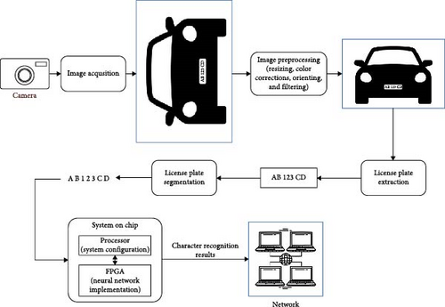
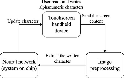
Continuous advances in neural networks, computer processing power, and field programmable gate array (FPGA) performance enabled a wide range of practical neural network applications [1]. They are mostly used in the approximation of nonlinear functions [2], pattern classification [3], data and image processing [4, 5], filtering [6], sequential decision-making [7], robotics [8], gesture recognition [9], chaotic time series analysis [10], multiphase flow measurements [11–13], etc. More specific application areas of neural networks in consumer electronic products include widely used plate license recognition systems [14, 15] and handwritten character or digit recognition solutions for postal mail sorting [16], bank check processing [17], and handwritten forms readout [18]. Furthermore, the application of deep neural networks (DNNs) exhibits rapid development in the Internet of Things (IoT) technology [19, 20], which places high demands in terms of resource constraints, such as limited memory capacity, weak computing capacity, and low battery capacity. One of the potential solutions to avoid migration of the DNN model to a remote cloud server is the integration of FPGA in IoT devices. Moreover, systems with critical time requirements, which implement some form of neural network, use graphics processing units (GPUs) to train and execute neural networks [21–23]. Because GPUs consume a significant amount of energy for the execution of operations in neural networks, the use of FPGAs and application-specific integrated circuits (ASICs) is becoming a significant alternative solution [24–26], including the recent FPGA-GPU hybrid acceleration platform [27]. Due to low power consumption, relatively low cost, and high performance achieved by a high degree of task parallelization and the development of specific purpose hardware, FPGAs have become more applicable in industrial applications recently. Although FPGAs were not widely used for the implementation of neural networks, recent contributions justify their benefits in terms of lower power consumption and improved performance [28, 29]. For the development of neural networks in pattern recognition applications, particularly for handwritten digit recognition, a relevant test and training database are required. There are several databases of handwritten digits available [30, 31], but many engineers and scientists have recognized the Modified National Institute of Standards and Technology database (MNIST) [32–34] as the most relevant and has become the standard in the field of pattern recognition [35], computer vision [36], and deep learning [37]. Although there have been many effective solutions to the problem of MNIST database digit classification for some time, it is still relevant to evaluate contributions in the field of neural network-based digit classification systems [38, 39]. The most efficient neural networks used to solve this problem are combinations of convolutional, recurrent, and fully connected neural networks. The accuracy of digit classification using such networks exceeds 99% [40]. Several recent FPGA-based contributions propose spiking neural networks (SNNs) for digit classification [41–44]. Due to its energy efficiency and great online training potential, SNN is a promising candidate for implementation in FPGA. Some of the recent contributions propose stochastic computing-based implementations, due to low hardware overhead potential [45, 46]. Most of the state-of-the-art FPGA-based solutions for handwritten digit recognition demand significant hardware resources, which motivated us to design a fully connected neural network along with the feedforward propagation (FP) and backward propagation (BP) algorithms on the available low-end development board while keeping the system as simple as possible. In this paper, we propose a neural network model for handwritten Arabic digit recognition, using an FPGA to process input images of 28 × 28 pixels, previously loaded into DDR3 memory. The MNIST database is used to train the neural network. We also propose the design of an FPGA-based digital system consisting of an FP block, a BP block, and a data path between the processing system (PS) and the programmable logic (PL). The digital system is designed in the Xilinx Vivado software suite, and the Very High-Speed Integrated Circuit Hardware Description Language (VHDL) is used for hardware description. The PS is programmed using the Xilinx SDK development environment. The proposed system can be used as a subsystem in a wide range of applications, where digit recognition is required. Moreover, it can also be extended for character recognition by performing training on relevant character datasets. Use cases of the potential application of the system are illustrated in Figure 1. Example of license plate recognition is depicted in Figure 1a, while Figure 1b shows an example of a real-time handwritten character recognition system using a handheld device. Accordingly, the number of neurons in the output layer has to be extended, while the neural network would have to be retrained using a dataset of letters and numbers from license plates, as proposed in Figure 1a. The proposed system for handwritten digit recognition is implemented and evaluated on the Zynq Board (ZYBO), and the percentage of correctly predicted digits is determined. Forward propagation and BP algorithm execution speeds were also measured. Finally, the results of the utilization of FPGA resources and the maximum power consumption of the FPGA system are presented. The performances of the proposed system are then compared with the relevant state-of-the-art FPGA solutions for handwritten digit recognition.
- •
Design of a fully connected neural network along with the FP and BP algorithms on the available low-end development board while keeping the system as simple as possible and as less intensive as possible for hardware resources.
- •
The system is highly independent; that is, it does not need any other communication with external devices besides a simple serial terminal application on the PC during runtime.
- •
Accommodation of general-purpose processor that allows runtime reconfigurability of the hardware accelerator during both inference and training phases.
2. Neural Network Model
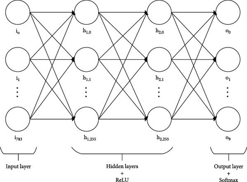
An artificial neural network is selected to solve the problem of digit classification from the MNIST database. The network consists of four fully connected layers: input, two hidden, and one output layer. An image from the MNIST database, with a resolution of 28 × 28 pixels, is fed to the input layer of the network. The specifications of the neural network are summarized in Table 1. As can be seen in Figure 2, the network model is flexible in terms of the possibility of changing the number of neurons in the layers and the number of hidden layers. The hidden layers implement the ReLU activation function, and the output layer implements the Softmax activation function.
| Number of fully connected layers | Four (input, two hidden, and one output) |
|---|---|
| Number of neurons in the input layer | 784 |
| Number of neurons in each hidden layer | 256 |
| Number of neurons in the output layer | 10 |
| Activation function in hidden layers | ReLU |
| Activation function in output layer | Softmax |
2.1. Network Input and Output
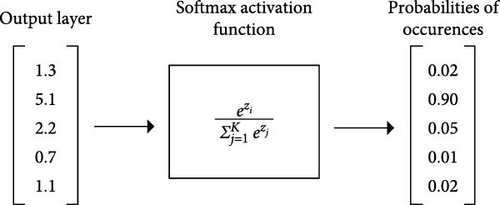
The pixel values of the images from the MNIST database are scaled between 0 and 255 and represented by an integer. The system proposed in this paper uses floating point numbers in the calculations, while the pixel values are standardized, that is, scaled between −1 and 1. Scaling the input data often helps to avoid unfavorable local minima during training and speeds up network training. Since the purpose of the system is to recognize Arabic numerals from 0 to 9, the output layer contains 10 neurons. The output of an individual neuron in the output layer represents the probability that a particular digit has been recognized in the image. For example, neuron o1 from Figure 2 represents the probability that digit 1 appears in the input image. The Softmax activation function, commonly used on the output layer to solve classification problems, gives the probability that a particular class will appear.
2.2. Activation Functions
2.3. FP Algorithm
2.4. BP Algorithm
Neural networks implement a BP algorithm with the goal of training network parameters (e.g., weights). The algorithm uses a chain rule to calculate the cost gradients in each part of the network and adjust the network parameters accordingly. Here, we provide a theoretical background for the implementation of the BP algorithm in an artificial neural network. Before running a BP algorithm, it is necessary to acquire the prediction error. The prediction error is calculated using the loss function. Furthermore, the loss is used when calculating the loss gradients, which are used to adjust the network parameters afterward. Some of the most commonly used loss functions are mean squared error, binary cross-entropy, categorical cross-entropy, and sparse categorical cross-entropy. A list of loss functions and appropriate expressions is shown in Table 2.
| Loss function | Expression |
|---|---|
| Mean squared error | |
| Binary cross-entropy | |
| Categorical cross-entropy | |
| Sparse categorical cross-entropy |
Using Expressions (9) and (5), new weight values can be calculated in the currently processed layer. An increase in the learning rate causes an increase in the speed of training, but a high value of the rate can cause an increase instead of a decrease in the total cost of training, which must be considered during the design of the system. Furthermore, a too low value of the rate can cause very slow training.
3. FPGA System Implementation
A digital system that includes data path, PS, and PL is implemented on the ZYBO development board. The system implemented in PL includes a module for executing the forward propagation algorithm, a module for executing the BP algorithm, and system management.
3.1. System Input and Output
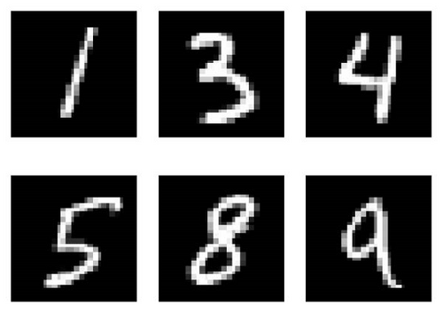
The input of the digit recognition system is the image containing the handwritten digit that should be recognized and classified at the output of the system, which is the result of the classification, that is, the digit most likely to be in the image. The input black-and-white image has a resolution of 28 × 28 pixels (Figure 4). The pixel is represented by 32-bit floating point arithmetic. The introduction of fixed-point arithmetic into the system is also possible, but it would require modifications of the complete system. Introducing fixed-point arithmetic enables a simpler and less resource-hungry system but causes a slight decrease in system accuracy at the same time. The digits contained in the decimal system are in the set [0,9] ∈ N so it follows that only one of these digits can appear at the output. Since the classification result is never completely accurate, that is, the system, as the result gives the digit with the highest probability of occurrence, the probability of occurrence of digits in the image can also be displayed along with the classification result.
3.2. Communication Between PS and PL
Communication between the PS and the PL is achieved by writing and reading data from the registers in the PL. The interface of the PS toward the PL, in this case, is realized through the AXI4-Lite protocol. AXI4-Lite is a simpler implementation of the Advanced eXtensible Interface 4 (AXI4) protocol that allows communication between a processor and a module in a PL that implements the AXI4-Lite interface. It is generally used when the processor writes or reads data from a register in the PL. Additionally, the AXI4-Lite interface contains address signals that allow access to any register in the PL (registers are addressed), using only one AXI4 interface on the PS. The main difference between the AXI4 and AXI4-Lite protocols is that AXI4-Lite does not support data stream transmission in a single transaction but only a single 32-bit or 64-bit data per transaction.
In this paper, the management of AXI direct memory access (DMA) IP cores is achieved with the AXI4-Lite protocol. The protocol enables communication with internal IP core registers such as control registers, status registers, and source and destination address registers. This allows the processor to initialize DMA transfers with all the necessary parameters. Figure 5 shows a block diagram of the connection between the PS and AXI DMA IP cores. From Figure 5, it can be seen that AXI DMA is connected to the PS only through the AXI4-Lite interface and interrupt signal, while through AXI4, it reads or writes data to DDR3 memory.
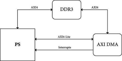
The interrupt signals, seen in Figure 5, also allow communication between the PS and the PL. The number of interrupt signals varies in such a manner that, for example, if the AXI DMA is set to include only the read channel, there is only one interrupt signal notifying the processor that the data reading is complete. If both the write channel and the read channel are on, there is an interrupt signal for both channels.
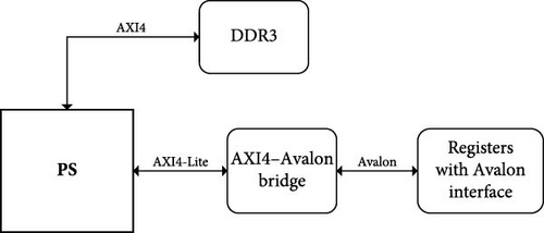
In addition to the internal registers of the AXI DMA IP core, particular registers in the digit recognition system control the entire system with an emphasis on the forward propagation module and the BP module. Access to these registers is provided by the Avalon protocol. Avalon has the same task as the AXI4-Lite protocol, but the implementation of the Avalon interface is somewhat simpler and takes up less FPGA system resources. Figure 6 shows a block diagram of the PS and registers connections to the Avalon interface. Because the PS communicates with PL using only the AXI4 interface, the system has a built-in IP core “AXI4-Avalon bridge” (Figure 6). This IP core performs the adjustment between two protocols.
3.3. Feedforward Module
The feedforward module implements functionalities to execute the forward propagation algorithm. Its main task is to read data from two FIFO memories, which store weights and outputs from neurons, and calculate the outputs from neurons in the next layer, based on the stored values.
Figure 7 shows the block diagram of the feedforward module. Communication between modules is achieved using the AXI4-Stream protocol. The synchronization block forwards the data to the multiplier if the data at the outputs of both FIFO memories are valid; that is, neither memory is empty. The product of the weight and the output from the neurons is then fed to the input of the last data detector, which, according to the given number of elements of the series of weights and the series of outputs from the neurons, informs the accumulator that the last data in the sequence are transmitted. The accumulator accumulates the products calculated in the multiplier up to the last data in the sequence. A valid accumulation result is activated in the activator and FIFO writer module if the signal to control the activation of the output from the neurons is active. The FIFO writer first saves it in FIFO and afterward via DMA to DDR3 memory.

The task of the synchronization module is to forward data from the AXI4-Stream input interfaces to the AXI4-Stream output interfaces. Data from DDR3 memory are written via DMA to FIFO memory modules from which the synchronization module reads data. The condition for forwarding data from the input to the output of the module is that both data at the input to the module are valid, from which it follows that neither FIFO is empty. Also, it is important to point out that due to the settings of the multiplier and the accumulator, which allow a nonblocking mode of operation of the AXI4-Stream protocol, a synchronization module was created. The nonblocking mode of the AXI4-Stream protocol prevents a two-way handshake. It follows that the nonblocking mode of the AXI4-Stream protocol implements a one-way handshake; that is, the sender module notifies the recipient that the data are valid and, without feedback on the readiness to receive the data, sends the data to the recipient.
The multiplier returns the result of two 32-bit operand multiplication, represented by floating-point arithmetic. The multiplication operation starts after the desired operands are placed on the data lines of the input AXI4-Stream interfaces, and the “valid” lines are activated during one period of the clock. It takes eight clock periods to calculate the result, but the structure of this model is a pipeline so that data can be fed to the input continuously. If data are continuously fed to the block, the first result will be delayed by eight clock periods, and then, when the pipeline is full, the results will appear consecutively each clock period. By activating the corresponding line, the output AXI4-Stream interface signals that the result is valid.
The task of the last data detector is to count the amount of data it has passed from input to output and in the clock period when the last data appear on the input AXI4-Stream interface and to activate the corresponding line on the output interface that signals the accumulator that it is receiving the last data in series. The behavior of the module is conditioned by the behavior of the accumulator. The length of a series of weights and outputs from neuron input allows for specifying the amount of data in the string.
The accumulator accumulates all products of the weights and outputs of the neurons from the previous layer and gives a valid accumulation result at the output. Accumulation is performed for each neuron in the currently calculated layer according to the forward propagation algorithm. The accumulator value is initially set to 0. If valid data are set to the data lines of the input AXI4-Stream interface, the value of the accumulator increases by the data value at the input. The last data in the input data series, indicated by the active state of the corresponding signal, signal to the accumulator to complete the accumulation process. When the accumulation process is complete, a valid accumulator value appears on the data lines of the AXI4-Stream output interface. After that, the accumulator value is set to 0 again, and the next accumulation procedure can be started.
The task of the activator and the FIFO writer is to activate the accumulation results and save the calculated outputs from neurons in FIFO memory from which they are stored in DDR3 memory via DMA. When valid data appears on the data lines of the input AXI4-Stream interface, activation is performed if the neuron output activation control signal is active. The activated data are then stored in FIFO memory. If the neuron output activation control signal is not active, the data are stored in the FIFO memory in its original state.
3.4. BP Module
The BP module implements functionalities for executing the BP algorithm. Its main task is to calculate new weight values in the currently processed layer of the network and error gradients for the next processed layer. The aforementioned module outputs are calculated based on the old weight values and neuron outputs stored in the last iteration of the propagation advance. Communication between individual modules is achieved by the AXI4-Stream protocol. The block diagram of the BP module is shown in Figure 8. The error multiplexer allows choosing between three error sources: Avalon register error, RAM 1 output, and RAM 2 output. The error source is different in each layer of the network. In the case of processing the output layer of the network, the data from the Avalon register—error—are fed to the input of the BP module via the error multiplexer. These errors are calculated in PS. The error gradients, calculated in the output layer for the next processed layer, are stored in RAM 1. It follows that during the next layer processing, the output of RAM 1 will be selected to the input of the BP module. In that layer, error gradients are calculated and stored to RAM 2, so that RAM 2 will be selected with an error multiplexer in the next layer calculation, etc.
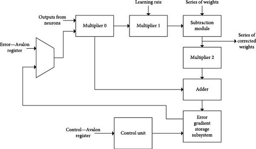
Multiplier 0 starts the operation of multiplying the output of the neurons and the error gradient when valid data appear on both data inputs of AXI4-Stream interfaces during the same clock period. The structure of the module is a pipeline, and valid data can be continuously fed to the input. The first result will appear at the output for as many clock periods as the latency parameter is set to. The module at the output provides an error gradient that further serves to calculate the corresponding weight correction. Multiplier 1 and multiplier 0 start a multiplication operation when both data at the module input are valid and the data can be fed to the input in succession. The task of this module is to multiply the learning rate by the appropriate error gradient and to give the correction of the appropriate weight at the output. The subtraction module performs the subtraction operation after valid data appear on the input AXI4-Stream interfaces during the same clock period. The structure of the module is also a pipeline and works in the same way as the multipliers mentioned above. The task of the module is to subtract the weight correction from the corresponding weight from the FIFO memory that stores the weights. The result is a new weight value that can be stored in DDR3 memory.
The task of the FIFO writer module is to write new weight values to the FIFO that stores the new weights. The write operation is done when there are valid data on the input AXI4-Stream interface. Multiplier 2 starts the multiplication operation when the data on the input AXI4-Stream interfaces are valid in the same clock period. The task of the module is to multiply the corresponding error and the value of the new weight to obtain an error gradient at the output for the next processed layer. This error gradient is the result of only one relationship between the currently processed layer and the next processed layer, and its value is not final at this stage. The task of the module FIFO–small buffer is to provide the adder with the ability to read valid data from the FIFO memory that stores neuron output. The multiplier 0 module reads 32 values from the aforementioned FIFO memory before valid data appear at the input of the adder. It follows that FIFO–small buffer saves these 32 values before the adder starts reading it.
The adder works in the same way as the multipliers and the subtraction module, and its structure is a pipeline. It is important to emphasize that in front of the adder, there is a synchronization block which, in addition to forwarding the operands to the adder, also takes a value from FIFO, a small buffer. If the value is equal to 0, the value of one of the operands is set to 0. Otherwise, the operand is set to the value obtained from multiplier 2. The adder’s task is to accumulate error gradients for the next processed network layer. The adder takes the error gradient for the corresponding neuron in the next processed layer and adds a new error gradient to it.
The block diagram of the error gradient storage subsystem is shown in Figure 9. Since the adder must be able to store the results in both RAM memories, a demultiplexer was created to enable setting the adder output to the input of RAM 1 or RAM 2, according to the selected input. Both RAMs in this subsystem are dual-port RAMs. The multiplexer provides the ability to select output from one of two RAMs. RAM controlling, in the form of permission to write and address memory, is performed by the aforementioned RAM controller.
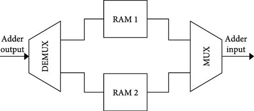
The task of the RAM controller is to control the writing and reading of data from both RAM memories and to address data. The control depends on the following inputs to the module: the number of neurons in the current layer, the number of neurons in the previous layer, the validity of the output from multiplier 2, the validity of the output from the adder, the last layer, and RAM selection. If the last layer is currently being processed, the error gradients for the next layer are written to RAM 1. Processing of the next layer changes the data in the RAM in which the error gradients are stored. Specifically, in one layer, error gradients are stored in RAM 1, errors are read from RAM 2, and then roles are changed in the next layer. The control unit of the BP module is a combinational circuit that generates output according to the 4-bit input vector that is connected to the control register via the Avalon interface. The processor accesses the control register to achieve the desired functionality of the BP module. Controlling the BP module involves initializing the gradients, notifying the module that calculations are being performed in the output layer of the network, selecting error gradients RAM, and starting to perform the propagation.
3.5. System Overview
The block diagram of the whole system can be seen in Figure 10. A wrapper, which realizes the data path from DDR3 memory to the previously mentioned modules and back, has been added to the previously described modules for forward and BP. The wrapper also allows communication between the processor system and PL. The entire system is controlled via the control register by the Avalon interface, that is, a certain system function is performed by writing particular data to it. Bit 5 (system function selection) of the control register allows for the selection of the data path in the system. Specifically, it allows the data path to go either through the forward propagation module or through the BP module. Bit 1 (start of propagation execution) should be activated when there is a need to start calculations in the BP module. By setting bit 2 (RAM selection) to the appropriate logic state, the RAM memory in the BP module is selected in which the error gradients are written for the next processed layer. By activating bit 3 (last layer), the BP module receives information that the last layer of the network (output) is currently being processed and operates accordingly. Activating bit 4 (gradient initialization) allows resetting the values in RAM for error gradients; that is, if error gradients for the next processed layer are currently calculated and accumulated, this bit is activated, and thus, new zero gradients are accumulated.

During the execution of the forward propagation algorithm, the data path is selected through the propagation module in advance, and bit 0 of the control register determines whether to activate the outputs of the currently processed neurons and then initiate DMA transfers of weights, neuron outputs, and calculated neuron outputs. The propagation block takes data from the FIFO memory in advance and saves the results in the FIFO, which are further stored in the DDR3 memory via DMA 2.
For the BP algorithm execution, the data path is selected through the BP module, and certain bits of the control register are set as required. DMA transfers of weights, neuron outputs, and corrected weights are then initiated. The BP block then takes the data from the FIFO memory modules and saves the corrected weights in FIFO which are further stored in DDR3 via DMA.
3.6. PS Application
The Zynq PS application is created in the Xilinx SDK development environment. Before starting the application, the following data must be written to DDR3 memory: a set of training images, a set of initialized weights, the expected outputs of the training set, and the expected outputs of the test set. The aforementioned data are recorded in large quantities, so a certain amount of memory is reserved for each data group. Intermediate results are also stored in memory: first-layer outputs, second-layer outputs, third-layer outputs, and a set of corrected weights. PS–PL communication is realized mainly through registers with the Avalon interface. The Xilinx SDK provides the base address of the AXI-Avalon bridge, and accordingly, the relative addresses of each register are determined. These addresses are located in the virtual address space.
Since the system has the ability to select the classification and training mode (PL setting), a register has been added to the system that has no impact on the operation of the system in the PL. When selecting the hardware mode and FPGA programming, this register is set to a certain state, and the processor reads the content of that register at a certain moment. According to the hardware settings, a certain part of the program is executed; for example, if the processor reads a value 1 from the register, the processor will manage the hardware so that the neural network is trained. The driver for the training mode of the hardware starts with the general system setup (declaration and initialization of variables, module configuration, and parameter entry). After the system is set up, the main loop follows in which the network training is performed; that is, one epoch of training is performed within one iteration of the loop. The main loop contains two loops, where, first, network training is performed over a set of training images. This includes the execution of the propagation algorithm, calculating the loss of the image, accumulating the loss of the training epoch, calculating the recognition error, and executing the BP algorithm. After completing the training epoch in the first loop, the network is tested over a set of test images in the second loop. This involves executing a forward propagation algorithm for each image in the test set, and at the end of the loop, calculating and displaying the percentage of accurately recognized digits. This completes one epoch of neural network training and executes the next if the network is not trained sufficiently. If it is trained sufficiently, the program is terminated.
The classification mode driver also starts with a general system setup and parameter entry. The loop then executes a forward propagation algorithm and increments the counter of correctly recognized digits for each image from the test set. The program ends after all images from the test set are processed, and the percentage of correctly recognized digits is calculated and displayed.
4. Results and Discussion
After synthesis and implementation in the Xilinx Vivado software suite, the complexity of the system has been evaluated. The system occupies 10,020 (57%) lookup tables, 7781 (22%) registers, 17 (21%) DSP blocks, and 3 (5%) BRAM blocks. The maximum power consumption of the system is 1.602 W, while the operating frequency of the system is 100 MHz.
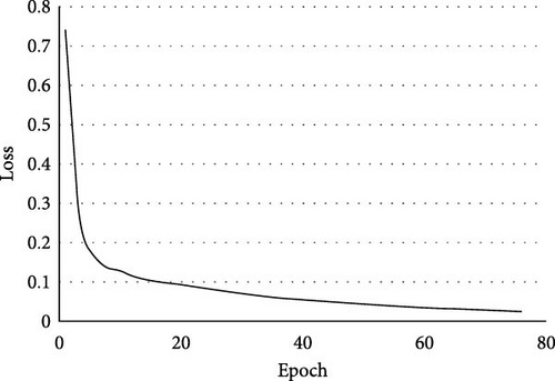
The network training procedure is set up as follows. PL is first programmed, followed by PS programming. Then, the following data are written to the memory using the “Dump/Restore Data File” option of the Xilinx SDK development environment: a set of weights initialized with the “He” method, a set of training images, a set of training reference data, a set of test images, and a set of test reference data. After entering the input data, the number of images for the network training is set, and the number of images for the network testing is set. Also, the learning rate is set, and finally, the network training is started. The training process is stopped after the percentage of accurate detections begins to fall steadily, and then a set of trained weights, following the epoch with the highest percentage of accurate identifications, is being stored in a binary file. The training was performed on 7000 images from the training set. The training set was balanced, and the distribution of the training samples for each class from 0 to 9, respectively, is as follows (784, 675, 716, 716, 610, 709, 754, 650, and 695). The learning rate was set to 0.0003. The training was completed after 77 epochs, lasting 2 h and 49 min. The change in loss function over epochs for the training set is shown in Figure 11. Testing was performed on 1000 images from the test set. The test set was balanced, and the distribution of the test samples for each class from 0 to 9, respectively, is as follows (126, 116, 107, 110, 87, 87, 99, 89, and 94). By testing a network on 1000 images from the test set, the data from which the confusion matrix is created (Table 3) are obtained. The percentage of accurate detections for the whole test set is 92.8%. Based on the confusion matrix, it can be seen that the network in 98% of cases accurately recognizes the digits “0” and “1,” while in 89% of cases accurately recognizes the digits “4” and “9.”
| Recognized (%) | |||||||||||
|---|---|---|---|---|---|---|---|---|---|---|---|
| 0 | 1 | 2 | 3 | 4 | 5 | 6 | 7 | 8 | 9 | ||
| Expected | 0 | 98 | 0 | 0 | 0 | 0 | 0 | 1 | 0 | 0 | 1 |
| 1 | 0 | 98 | 0 | 0 | 0 | 0 | 1 | 0 | 1 | 0 | |
| 2 | 0 | 0 | 91 | 0 | 1 | 0 | 0 | 3 | 4 | 0 | |
| 3 | 1 | 0 | 2 | 91 | 0 | 4 | 1 | 1 | 1 | 0 | |
| 4 | 0 | 0 | 1 | 0 | 89 | 0 | 1 | 0 | 4 | 5 | |
| 5 | 1 | 0 | 0 | 1 | 0 | 93 | 1 | 0 | 2 | 1 | |
| 6 | 3 | 0 | 1 | 0 | 1 | 0 | 92 | 1 | 1 | 0 | |
| 7 | 0 | 2 | 3 | 1 | 1 | 0 | 0 | 92 | 0 | 1 | |
| 8 | 0 | 0 | 0 | 3 | 1 | 0 | 0 | 1 | 94 | 0 | |
| 9 | 0 | 1 | 0 | 1 | 2 | 0 | 0 | 4 | 2 | 89 | |
The execution time of the forward propagation algorithm was equal to 7.7 ms, while the execution time of the BP algorithm was equal to 16.3 ms. The theoretical number of clock periods required to execute the propagation algorithm in advance was equal to 274,080, while in the actual implementation of the algorithm, it was equal to 772,310. Also, the theoretical number of clock periods required to execute the BP algorithm was equal to 289,680, while in the actual implementation of the algorithm, it is equal to 1,637,748. The difference appears due to idle time in DMA transfers, the time required for writing to registers with the Avalon interface, and executing the rest of the program on the processor, which is not included in the theoretical number of clock periods. The problem of significant difference between a theoretical number of clocks and a number of clocks in real implementation could be partially solved by optimizing the driver in ZYNQ PS or designing a new DMA module that could provide better throughput since the existing Xilinx IP is already set to the largest possible data burst size. Another way to solve this problem is to redesign the data flow path in the system by introducing prefetch buffers in the system to reduce idle time in DMA transfers.
A comparison of the proposed neural network with the state-of-the-art FPGA-based neural networks for handwritten digit recognition is provided in Table 4. The paper [24] represents the implementation of a system for handwritten digit recognition using a convolutional neural network. It achieves higher accuracy and lower execution time compared to this work, due to its network structure that generally achieves better results in handwritten digit recognition applications, higher clock frequency, and parallelization. However, it requires more extensive utilization of hardware resources. In comparison to this work, it utilizes six times more registers and 16 times more DSP cores, and it does not implement a BP algorithm. The paper [25] represents the implementation of a system for handwritten digit recognition using a binarized convolutional neural network.
| LUT | FF | DSP | LE ALMa |
BRAM | Power (W) |
Accuracy (%) |
Frequency (MHz) |
Data | FP time (ms) |
BP | BP time (ms) |
|
|---|---|---|---|---|---|---|---|---|---|---|---|---|
| [24] | 12,588 | 48,765 | 274 | — | — | — | 97.57 | 150 |
|
0.0176 | No | — |
| [25] | — | — | — | — | — | 0.136 | 85 | 100 | 1-bit | 0.18 | No | — |
| [26]b | — | — | — | 34,000 | — | — | 89 | 25 |
|
N/A | Yes | N/A |
| [26]c | — | — | — | 183d | — | — | 89.6 | 250 |
|
20 | No | — |
| [26]e | — | — | — | 428d | — | — | 92.7 | 60 |
|
150 | No | — |
| [39] | 44,668 | 14,274 | 604 | — | — | 566.3 | 95.25 | 100 |
|
0.0016 | No | — |
| [42] | 75,996 | 77,580 | 0 | — | — | 1.25 | 95.3 | 100 | 13-bit | 0.27 | Yes | 1.22 |
| [43] | 39,514 | 56,036 | 82 | — | 180 | 2.42 | 98.98 | 100 |
|
3.18 | No | — |
| This work | 10,020 | 7781 | 17 | — | 12 KB | 1.6 | 92.8 | 100 |
|
7.7 | Yes | 16.3f |
- aLogic element adaptive logic module.
- bTwo layers, training on board.
- cTwo layers, training on the computer.
- dOccupation of logical elements by arithmetic logic unit.
- eThree layers, training on computer.
- fBackward propagation execution time (weight adjustment in the network done once).
The main advantage of this kind of neural network is the simplicity of mathematical operations that are performed on 1-bit binary numbers. Arithmetic logic units are simple and utilize a small amount of hardware resources. Compared to this work, the execution time of the feedforward algorithm is shorter due to system parallelization and simpler network structure. In addition, the system described in [25] does not implement a BP algorithm. The paper [26] presents the implementation of an artificial neural network, a multilayer perceptron, for handwritten digit recognition. Two network structures are represented: two layers and three layers. Arithmetic logic units are simpler compared to the implementation proposed in this work since they perform operations on 8-bit fixed-point data. Compared with our implementation in terms of accurate recognition percentage, the two-layer implementation in [26] achieves worse results, while the three-layer implementation achieves better results compared to this work. Feedforward algorithm execution times in the paper [26] are greater than one in our implementation.
The paper [39] also presents the implementation of a multilayer perceptron for digit recognition. The system consumes four times more “lookup” tables compared to this work, two times more registers, and 35 times more DSP blocks, which makes it more complex. It detects digits faster and more accurately, but it consumes 353 times more power, and it does not implement a BP algorithm. SNN-based implementations, proposed in [42, 43], provide better performance in terms of accuracy and computing time, compared to our implementation. Better performance in competing solutions is achieved by the higher factor of parallelization in the system, which leads to much higher hardware resource occupation. Implementation [43] does not implement a BP algorithm, occupies more hardware resources, and consumes more power than our implementation. The implementations proposed in [24, 39, 42, 43], due to their complexity, would not fit into the development board used in this work. The advantage of our work is that with limited resources for the acquisition and capacity of the development board, satisfactory performances were achieved. Porting the system to a smaller FPGA could partially resolve the problem of wasting static power but could also result in greater hardware resource occupation by increasing constraints for optimal signal routing through FPGA at the same time, which might reduce a maximal frequency of a system clock. ZYNQ PS is used for system configuration during runtime and data flow management since it is already embedded in the same chip as the FPGA. Therefore, it consumes some static power even when it is not included in the system. The inclusion of ZYNQ PS in the system brings up the simplicity of the system and usefully consumes power that would otherwise be wasted as static power. The advantages of having a system on a chip that includes a dedicated processor and FPGA are in offloading the FPGA in the form of system management and in the fact that ASICs, such as the ARM processor in our case, can operate at a much higher frequency than the soft-core processors in the FPGA. A general-purpose processor allows the run-time reconfigurability of the hardware accelerator during both inference and training phases in the proposed system. On the contrary, the design [39], which is implemented on a Virtex 7 chip using only PL, does not have this contribution.
The greatest contribution and advantage of the system, proposed in this paper, is in use cases for battery-powered devices, where power consumption is a critical parameter and where BP is a desirable functionality. An example of such an application use case is depicted in Figure 1b. For the handheld device, the solution proposed in the work [39] is not suitable because it consumes 566.3 W of power, while the solution proposed in this paper consumes 1.6 W, which is 353 times lower power consumption for the price of 2.45% lower accuracy. On the other hand, despite lower power consumption, the solution from [42] consumes ~7.5 times more lookup tables and flip flops to gain a 2.50% accuracy improvement compared to the system proposed in this paper. Besides the system proposed in this paper, only the systems proposed in [26]b and [42] enable BP, which is required to enable a neural network to learn and adapt to a specific handheld user and become more accurate.
The solution proposed in this paper can process 129 characters per second if BP is not used and 61 character per second if BP is used. Despite faster processing of the systems proposed in [39, 42] and [43], there is no benefit for application in a handheld device for real-time character recognition, since human writing speed cannot attain 190 characters per minute [47].
5. Conclusions
In this paper, an FPGA-based handwritten digit recognition system is proposed. The proposed system aims to implement a fully connected neural network on the low-end development board, thus keeping the system as simple as possible. The neural network model, including the forward propagation algorithm and the BP algorithm, is designed and fully implemented in the FPGA environment, enabling network training in the FPGA development system. The ARM processor is used to enable operation at a higher frequency and to allow for runtime reconfigurability of the hardware accelerator during both inference and training phases. In comparison with the relevant state-of-the-art solutions, this implementation achieves competitive results in terms of recognition accuracy and algorithm execution speed while maintaining system simplicity and low hardware resource consumption at the same time. Solutions proposed in [24–26, 39] are more focused on decreasing recognition execution time by parallelizing computing blocks, thus utilizing more hardware resources.
This work presents a power-efficient solution that consumes fewer resources and implements BP for improved adaptability to specific users while maintaining a relatively small tradeoff in accuracy and sufficient execution time.
Conflicts of Interest
The authors declare no conflicts of interest.
Funding
This research was funded in part by the Faculty of Electrical Engineering, Computer Science and Information Technology Osijek under the scientific projects “Neural networks in FPGA systems” and “Adaptation of the deep learning models for application in ADAS algorithms” and the J.J. Strossmayer University of Osijek under the project UNIOS-ZUP 2018-6.
Open Research
Data Availability Statement
The data are not freely available due to commercial confidentiality.


